

MICREL MIC58P42BWM, MIC58P42BN, MIC58P42BV Datasheet
MIC58P42 Micrel
MIC58P42
8-Bit Serial-Input Protected Latched Driver
General Description
The MIC58P42 serial-input latched driver is a high-voltage
(80V), high-current (500mA) integrated circuit comprised of
eight CMOS data latches, a bipolar Darlington transistor
driver for each latch, and CMOS control circuitry for the
common STROBE, CLOCK, SERIAL DATA INPUT, and
OUTPUT ENABLE functions. Similar to the MIC5842, additional protection circuitry supplied on this device includes
thermal shutdown, under voltage lockout (UVLO), and overcurrent shutdown.
The bipolar/CMOS combination provides an extremely lowpower latch with maximum interface flexibility. The MIC58P42
has open-collector outputs capable of sinking 500 mA and
integral diodes for inductive load transient suppression with
a minimum output breakdown voltage rating of 80V (50V
sustaining). The drivers can be operated with a split supply,
where the negative supply is down to –20V and may be
paralleled for higher load current capability.
With a 5V logic supply, the MIC58P42 will typically operate at
better than 5MHz. With a 12V logic supply, significantly
higher speeds are obtained. The CMOS inputs are compatible with standard CMOS, PMOS, and NMOS circuits. TTL
circuits may require pull-up resistors. By using the serial data
output, drivers may be cascaded for interface applications
requiring additional drive lines.
Features
• 3.3 MHz Minimum Data-Input Rate
• CMOS, PMOS, NMOS, and TTL Compatible
• Internal Pull-Up/Pull-Down Resistors
• Low Power CMOS Logic and Latches
• High Voltage (80V) Current-Sink Outputs
• Output Transient-Protection Diodes
• Single or Split Supply Operation
• Thermal Shutdown
• Under-Voltage Lockout
• Per-Output Over-Current Shutdown (500mA typical)
Ordering Information
Part Number Temperature Range Package
MIC58P42BN –40°C to +85°C 18-Pin Plastic DIP
MIC58P42BV –40°C to +85°C 20-Pin PLCC
MIC58P42BWM –40°C to +85°C 18-Pin Wide SOIC
Each of these eight outputs has an independent over current
shutdown of 500 mA. Upon over-current detection, the
affected channel will turn OFF until VDD is cycled or the
ENABLE/RESET pin is pulsed high. Current pulses less than
2µs will not activate current shutdown. Temperatures above
165°C will shut down the device. The UVLO circuit prevents
operation at low VDD; hysteresis of 0.5V is provided. See the
MIC59P60 for a similar device that additionally provides an
error flag output.
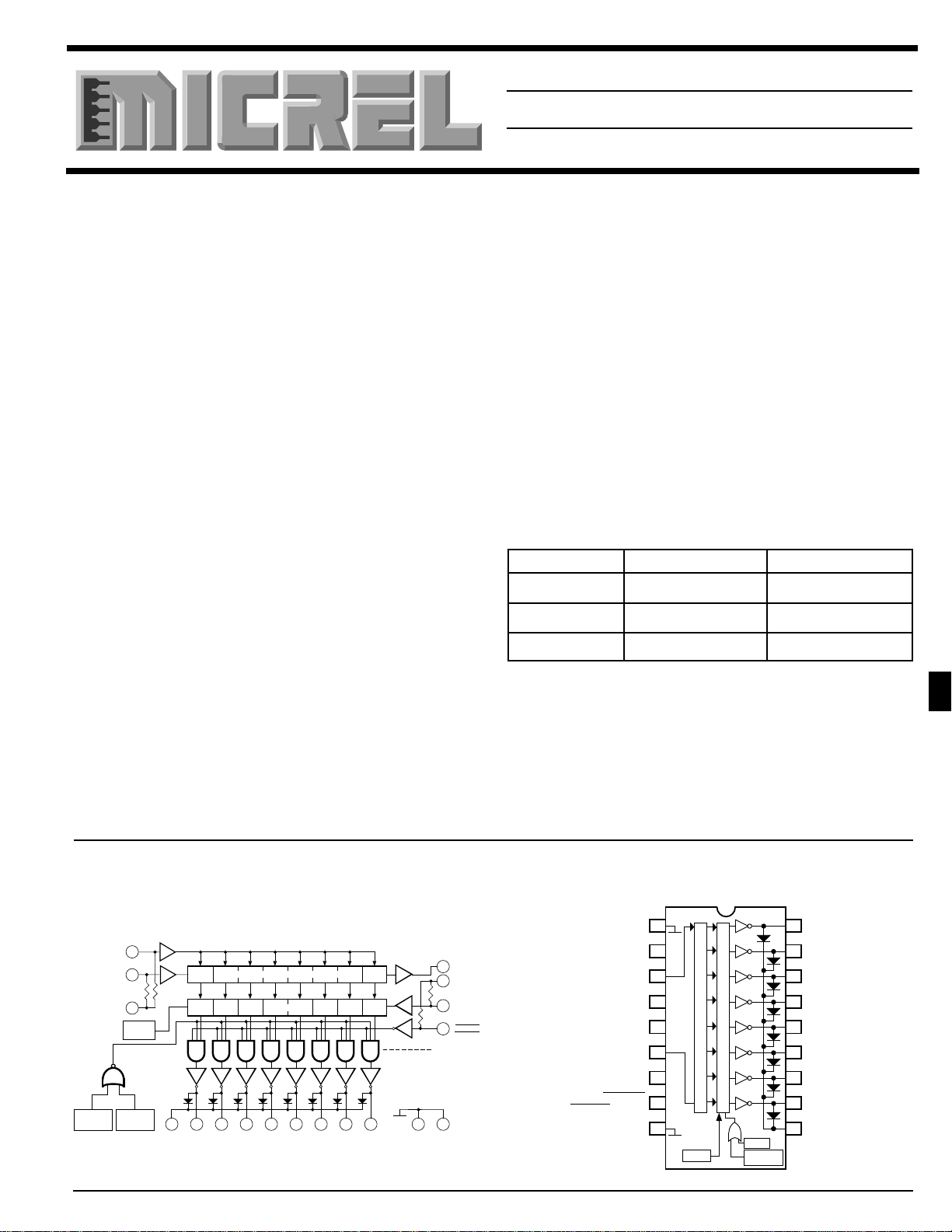
Functional Diagram
CLOCK
SERIAL
DATA IN
THERMAL
SHUTDOWN
2
3
V
4
SS
UVLO
I
LIMIT
K OUT
8-BIT SERIAL–PARALLEL SHIFT REGISTER
LATCHES
OUT
OUT
OUT
OUT
1
3
2
MOS
BIPOLAR
SUB
OUT
OUT
OUT
6
5
4
8
7
1
V
EE
SERIAL DATA OUT
6
5
V
DD
7
STROBE
8
OUTPUT
ENABLE/RESET
910 1112131415161718
Pin Configuration
(DIP and SOIC)
V
1
EE
CLOCK
2
SERIAL DATA IN
SERIAL DATA OUT
STROBE
OUTPUT
ENABLE/RESET
3
V
4
SS
V
DD
5
6
7
8
V
9
EE
SUB
SHIFT REGISTER
SUB
UVLO
LATCHES
I LIMIT
THERMAL
SHUTDOWN
7
OUT
18
1
OUT
17
2
OUT
16
3
OUT
15
4
OUT
14
5
OUT
13
6
OUT
12
7
OUT
11
8
K
10
October 1998 7-49
MIC58P42 Micrel
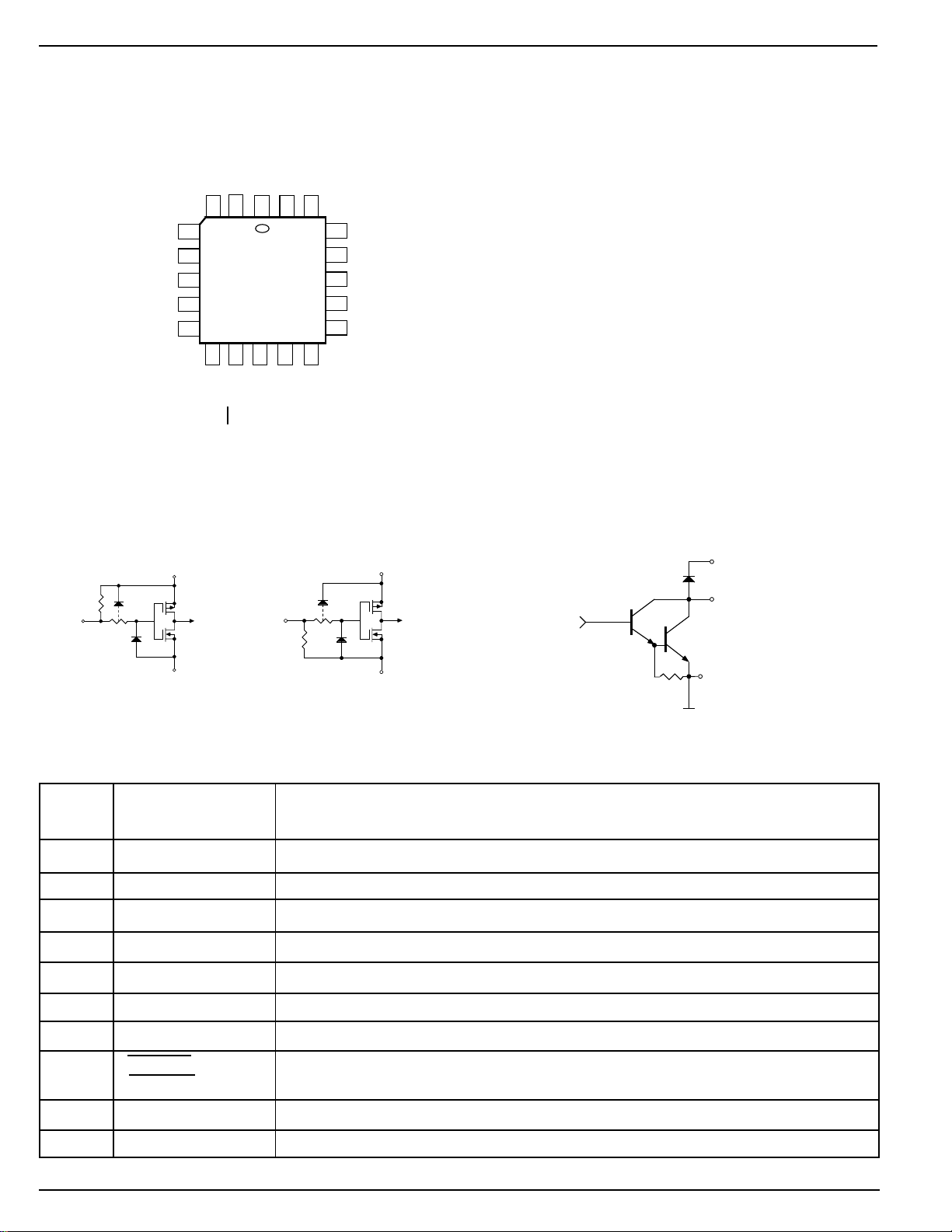
PLCC Pin Configuration
SERIAL DATA IN
CLOCK
2
3
NC
4
V
5
SS
V
DD
SERIAL DATA OUT
NC
MIC58P42BV
6
7
8
9 10
STROBE
OE/RESET
Typical Input Circuits
Absolute Maximum Ratings (Note 1, 2)
at 25°C Free-Air Temperature and VSS = 0V
Output Voltage 80V
Output Voltage, V
CE(SUS)
Logic Supply Voltage Range, V
EE
OUT 1
20 19
12 1311
K
OUT 2
18
17
16
15
14
OUT 8
OUT 3
OUT 4
OUT 5
OUT 6
OUT 7
V
1
EE
V
VDD with Reference to V
Emitter Supply Voltage (Substrate), V
Input Voltage Range, V
Package Power Dissipation, P
MIC58P42BN 1.82W
Derate above TA = +25°C 18mW/°C
MIC58P42BV 1.4W
Derate above TA = +25°C 14mW/°C
MIC58P42BWM 1.2W
Derate above TA = +25°C 12mW/°C
Operating Temperature Range, T
Storage Temperature Range, T
Note 1:For Inductive load applications.
Note 2: CMOS devices have input-static protection but are susceptible to
damage when exposed to extremely high static electrical
charges.
(Note 1) 50V
4.5V to 15V
–55°C to +125°C
–65°C to +150°C
IN
DD
EE
EE
–0.3V to VDD + 0.3V
D
A
S
25V
–20V
Typical Output Driver
SUB
K
NOUT
V
EE
STROBE
OUTPUT
ENABLE
V
V
DD
CLOCK
SERIAL
DATA IN
V
SS
DD
V
SS
3K
Pin Description
Pin Name Description
(DIP & S.O.)
1,9 V
EE
2 CLOCK Serial Data Clock. A CLEAR input must also be clocked into the latches.
3 SERIAL DATA IN Serial Data Input pin.
4V
5V
SS
DD
6 SERIAL DATA OUT Serial Data Output pin. (Flow–through).
Substrate. Most Negative voltage in the system connects here.
Logic reference (Ground) pin.
Logic Positive Supply voltage.
7 STROBE Output Strobe pin. Loads output latches when high. Strobe is needed to clear latch.
8 OUTPUT When Low, Outputs are active. When High, device is reset from a fault condition.
ENABLE/RESET
10 K Transient suppression diode's cathode common pin.
11—18 OUTPUT N Open Collector outputs 8 through 1.
7-50 October 1998
 Loading...