

General Description
Using BiCMOS technology, the MIC5841/5842 integrated
circuits were fabricated to be used in a wide variety of
peripheral power driver applications. The devices each
have an eight-bit CMOS shift register, CMOS control
circuitry, eight CMOS data latches, and eight bipolar
current-sink Darlington output drivers.
These two devices differ only in maximum voltage ratings.
The MIC5842 offers premium performance with a
minimum output breakdown voltage rating of 80V (50V
sustaining). The drivers can be operated with a split supply
where the negative supply is down to –20V.
The 500mA outputs, with integral transient-suppression
diodes, are suitable for use with lamps, relays, solenoids
and other inductive loads.
These devices have improved speed characteristics. With
a 5V logic supply, they will typically operate faster than
5 MHz. With a 12V supply, significantly higher speeds are
obtained. The CMOS inputs are compatible with standard
CMOS, PMOS, and NMOS logic levels. TTL or DTL
circuits may require the use of appropriate pull-up
resistors. By using the serial data output, the drivers can
be cascaded for interface applications requiring additional
drive lines.
MIC5841/5842
8-Bit Serial-Input Latched Drivers
The MIC5840 family is available in DIP, PLCC, and SOIC
packages. Because of limitations on package power
dissipation, the simultaneous operation of all drivers at
maximum rated current might require a reduction in duty
cycle. A copper-alloy lead frame provides for maximum
package power dissipation.
Features
• 3.3 MHz Minimum Data-Input Rate
• CMOS, PMOS, NMOS, TTL Compatible
• Internal Pull-Up/Pull-Down Resistors
• Low-Power CMOS Logic and Latches
• High-Voltage Current-Sink Outputs
• Output Transient-Protection Diodes
• Single or Split Supply Operation
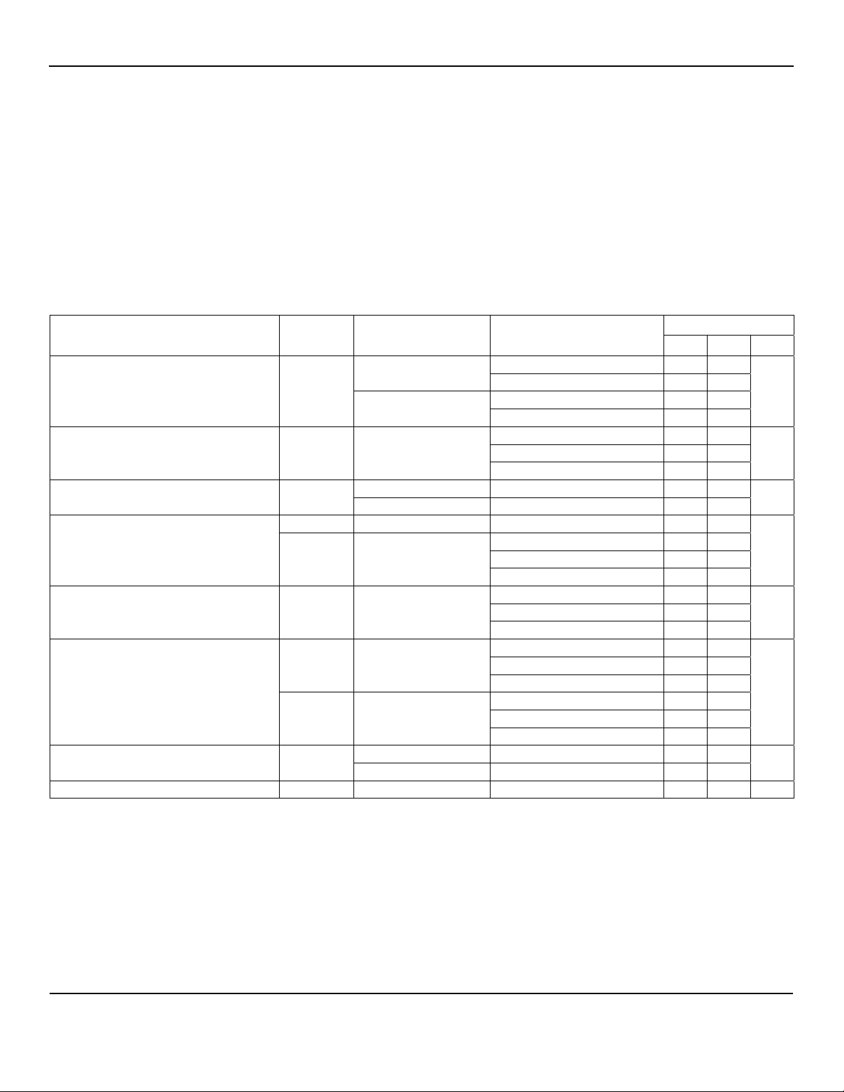
Ordering Information
Part Number
Standard Pb-Free
MIC5841BN MIC5841YN
MIC5841BV MIC5841YV
MIC5841BWM MIC5841YWM
MIC5842BN MIC5842YN
MIC5842BV MIC5842YV
MIC5842BWM MIC5842YWM
Micrel Inc. • 2180 Fortune Drive • San Jose, CA 95131 • USA • tel +1 (
May 2006
Temperature Range Package
–40ºC to +85ºC
–40ºC to +85ºC
–40ºC to +85ºC
–40ºC to +85ºC
–40ºC to +85ºC
–40ºC to +85ºC
18-Pin Plastic DIP
20-Pin PLCC
18-Pin Wide SOIC
18-Pin Plastic DIP
20-Pin PLCC
18-Pin Wide SOIC
408
) 944-0800 • fax + 1 (408) 474-1000 • http://www.micrel.com
M9999-050506
(408) 955-1690
Micrel, Inc. MIC5841/42
E
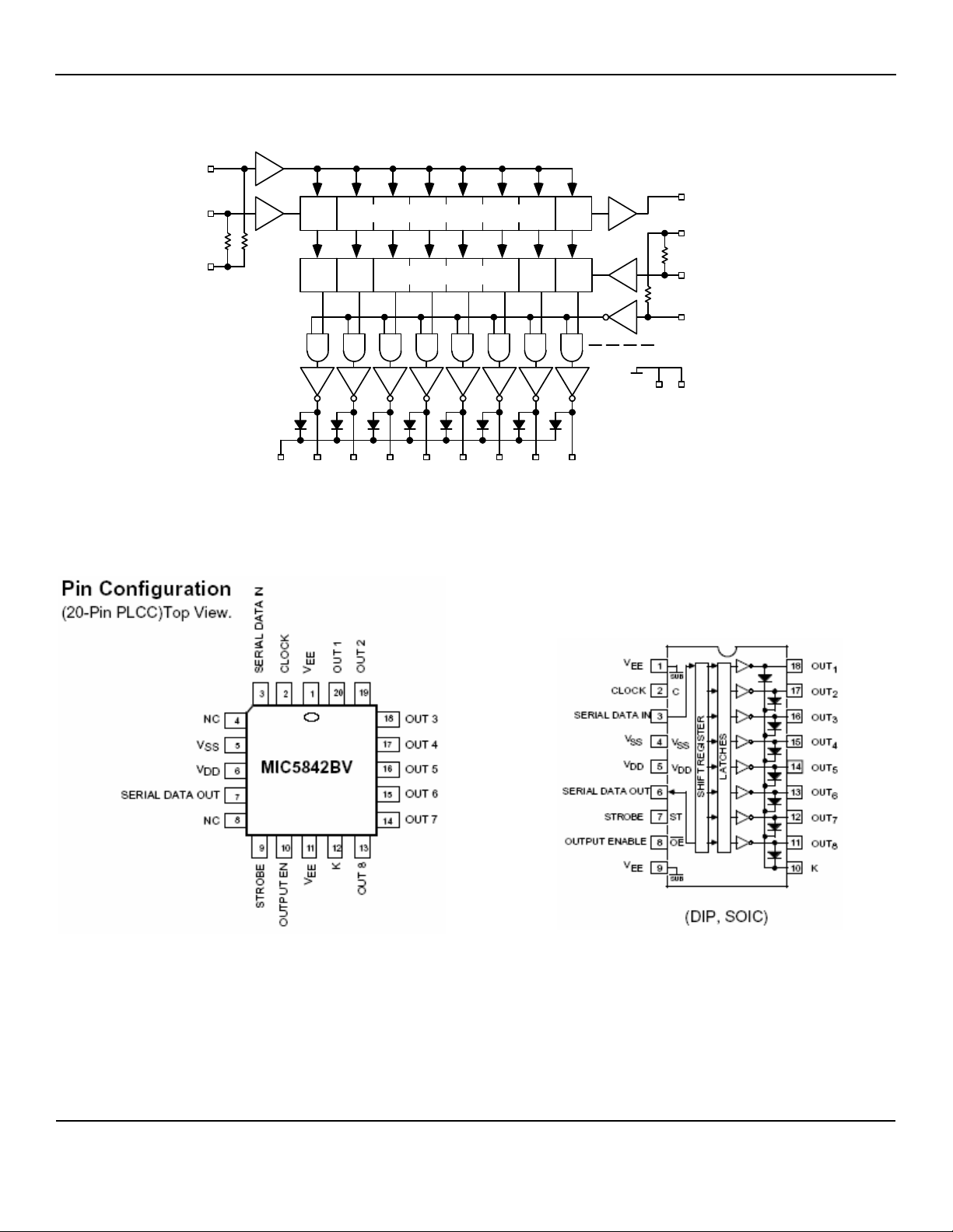
Functional Diagram
CLK
1
SERIAL
6
SERIAL
DATA IN
V
SS
3
4
8-BIT SERIAL-PARALLEL SHIFT REGISTER
LATCHES
MOS
Bipolar
Sub
DATA OUT
V
DD
5
STROBE
7
OUTPUT ENABL
8
(ACTIVE LOW)
1
9
V
EE
10
OUT
K
1
OUT
2
OUT
3
OUT
OUT
5
4
OUT
6
OUT
11
12131415161718
OUT
8
7
May 2006
2
M9999-050506
(408) 955-1690
Micrel, Inc. MIC5841/42
Absolute Maximum Ratings
At 25°C Free-Air Temperature and V
Output Voltage, V
(MIC5841) ............................. 50V
CE
(1,2,3)
................... 0V
SS
(MIC5842) .............................. 80V
Output Voltage, V
CE(SUS)
(MIC5841)
(1)..................................
35V
(MIC5842) ........................ 50V
Logic Supply Voltage, V
VDD with Reference to V
Electrical Characteristics
At TA = 25°C VDD = 5V, VSS = VEE = 0V (unless otherwise noted)
Characteristic Symbol Applicable Devices Test Conditions
Output Leakage Current I
Collector-Emitter Saturation Voltage V
Input Voltage
Input Resistance RIN Both
Supply Current
Clamp Diode Forward Voltage VF Both IF = 350mA 2.0 V
....................................... 15V
DD
..................................... 25V
EE
CEX
Both
CE(SAT)
(5)
CE(SUS)
V
IN(0)
V
IN(1)
IDD
IDD
Both 0.8
Both
Both
(ON)
Both
(OFF)
MIC5842
MIC5841 I
MIC5842 I
MIC5841 VR = 50V 50 Clamp Diode Leakage Current IR
MIC5842 V
Emitter Supply Voltage, V
Input Voltage Range, V
Continuous Output Current, I
Package Power Dissipation, P
...................................–20V
EE
............... –0.3V to VDD + 0.3V
IN
OUT
(2)
D
Operating Temperature Range, T
Storage Temperature Range, T
S
V
= 50V 50 MIC5841
OUT
= 50V, TA = +70ºC 100
V
OUT
V
= 80V 50
OUT
V
= 80V, TA = +70ºC 100
OUT
I
= 100mA 1.1
OUT
I
= 200mA 1.3
OUT
I
= 350mA, VDD = 7.0V 1.6
OUT
= 350mA, L = 2mH 35 Collector-Emitter Saturation Voltage V
OUT
= 350mA, L = 2mH 50
OUT
VDD = 12V 10.5
VDD = 10V 8.5
VDD = 5.0V(4) 3.5
VDD = 12V 50
VDD = 10V 50
V
= 5.0V 50
DD
All Drivers ON, VDD = 12V 16
All Drivers ON, VDD = 10V 14
All Drivers ON, VDD = 5.0V 8.0
All Drivers OFF, VDD = 12V 2.9
All Drivers OFF, VDD = 10V 2.5
All Drivers OFF, V
= 80V 50
R
= 5.0V 1.6
DD
.........................500mA
........................1.82W
.......–55°C to +85°C
A
........–65°C to +150°C
Limits
Min Max Unit
µA
V
V
V
kΩ
1.6
µA
May 2006
3
M9999-050506
(408) 955-1690

Micrel, Inc. MIC5841/42
Electrical Characteristics
At TA = –55°C VDD = 5V, VSS = VEE = 0V (unless otherwise noted)
Characteristic Symbol Test Conditions
Output Leakage Current I
Collector-Emitter Saturation Voltage V
Input Voltage
Input Resistance RIN
Supply Current
Limits
Min Max Unit
V
CEX
CE(SAT)
V
0.8
IN(0)
V
IN(1)
= 80V 50 µA
OUT
I
= 100mA 1.3
OUT
I
= 200mA 1.5
OUT
I
= 350mA, VDD = 7.0V 1.8
OUT
VDD = 12V 10.5
= 5.0V 3.5
V
DD
VDD = 12V 35
VDD = 10V 35
VDD = 5.0V 35
I
DD(ON)
All Drivers ON, VDD = 12V 16
mA
All Drivers ON, VDD = 10V 14
I
DD(OFF)
All Drivers ON, V
All Drivers OFF, VDD = 12V 3.5
All Drivers OFF, V
= 5.0V 10
DD
= 5.0V 2.0
DD
Electrical Characteristics
At TA = +125°C VDD = 5V, VSS = VEE = 0V (unless otherwise noted)
Characteristic Symbol Test Conditions
Output Leakage Current I
Collector-Emitter Saturation Voltage V
Input Voltage
Input Resistance RIN
Supply Current
Notes:
1. For Inductive load applications.
2. Derate at the rate of 18.2mW/°C above TA = 25°C (Plastic DIP)
3. CMOS devices have input-static protection but are susceptible to damage when exposed to extremely high static electrical charges.
4. Operation of these devices with standard TTL may require the use of appropriate pull-up resistors to insure an input logic HIGH.
5. Not 100% tested. Guaranteed by design.
Limits
Min Max Unit
V
CEX
CE(SAT)
V
0.8
IN(0)
V
IN(1)
= 80V 500 µA
OUT
I
= 100mA 1.3
OUT
I
= 200mA 1.5
OUT
I
= 350mA, VDD = 7.0V 1.8
OUT
VDD = 12V 10.5
= 5.0V 3.5
V
DD
VDD = 12V 50
VDD = 10V 50
V
= 5.0V 50
DD
I
DD(ON)
All Drivers ON, VDD = 12V 16
mA
All Drivers ON, VDD = 10V 14
I
DD(OFF)
All Drivers ON, V
All Drivers OFF, VDD = 12V 2.9
All Drivers OFF, V
= 5.0V 8
DD
= 5.0V 2.1.6
DD
MIC5841A VR = 50V 1.6 µA Clamp Diode Leakage Current IR
MIC5842A V
= 80V 100
R
V
V
kΩ
V
V
kΩ
May 2006
4
M9999-050506
(408) 955-1690

Micrel, Inc. MIC5841/42
Timing Conditions
(TA = 25°C Logic Levels are VDD and VSS) VDD = 5V
A. Minimum Data Active Time Before Clock Pulse (Data Set-Up Time)...................................................................... 75 ns
B. Minimum Data Active Time After Clock Pulse (Data Hold Time) ............................................................................ 75 ns
C. Minimum Data Pulse Width ................................................................................................................................... 150 ns
D. Minimum Clock Pulse Width................................................................................................................................... 150 ns
E. Minimum Time Between Clock Activation and Strobe ........................................................................................... 300 ns
F. Minimum Strobe Pulse Width.................................................................................................................................. 100 ns
G. Typical Time Between Strobe Activation and Output Transition............................................................................ 500 ns
SERIAL DATA present at the input is transferred to the shift register on the logic “0” to logic “1” transition of the CLOCK
input pulse. On succeeding CLOCK pulses, the registers shift data information towards the SERIAL DATA OUTPUT. The
SERIAL DATA must appear at the input prior to the rising edge of the CLOCK input waveform.
Information present at any register is transferred to its respective latch when the STROBE is high (serial-to-parallel
conversion). The latches will continue to accept new data as long as the STROBE is held high. Applications where the
latches are bypassed (STROBE tied high) will require that the ENABLE input be high during serial data entry.
When the ENABLE input is high, all of the output buffers are disabled (OFF) without affecting information stored in the
latches or shift register. With the ENABLE input low, the outputs are controlled by the state of the latches.
MIC5840 Family Truth Table
Serial
Data
Input
L = Low Logic Level
H = High Logic Level
X = Irrelevant
P = Present State
R = Previous State
May 2006
Clock
Input
H H R1 R2 … R7 R7
L L R1 R2 … R7 R7
X R1 R2 R3 … R8 R8
Shift Register Contents Latch Contents Output Contents
I1 I2 I3 … I8
X X X … X X L R1 R2 R3 … R8
P1 P2 P3 … P8 P8 H P1 P2 P3 … P8 L P1 P2 P3 … P8
X X X … X H H H H … H
Serial
Data
Output
Strobe
Input
I1 I2 I3 … I8
5
Output
Enable
I1 I2 I3 …I8
M9999-050506
(408) 955-1690

Micrel, Inc. MIC5841/42
Typical Output Driver
Typical Input Circuits
Maximum Allowable Duty Cycle (Plastic DIP)
VDD = 5.0V
Number of Outputs ON
(I
= 200mA
OUT
= 5.0V)
V
DD
8 85% 72% 64% 55% 46%
7 97% 82% 73% 63% 53%
6 100% 96% 85% 73% 62%
5 100% 100% 100% 88% 75%
4 100% 100% 100% 100% 93%
3 100% 100% 100% 100% 100%
2 100% 100% 100% 100% 100%
1 100% 100% 100% 100% 100%
VDD = 12V
Number of Outputs ON
= 200mA
(I
OUT
V
= 12V)
DD
8 80% 68% 60% 52% 44%
7 91% 77% 68% 59% 50%
6 100% 90% 79% 69% 58%
5 100% 100% 95% 82% 69%
4 100% 100% 100% 100% 86%
3 100% 100% 100% 100% 100%
2 100% 100% 100% 100% 100%
1 100% 100% 100% 100% 100%
May 2006
25ºC 40ºC 50ºC 60ºC 70ºC
25ºC 40ºC 50ºC 60ºC 70ºC
Max. Allowable Duty Cycle at Ambient Temperature of
Max. Allowable Duty Cycle at Ambient Temperature of
6
M9999-050506
(408) 955-1690

Micrel, Inc. MIC5841/42
Typical Applications
Relay/Solenoid Driver MIC5842 MIC5841 Hammer Driver
MIC5841 Solenoid Driver with Output Enable MIC5841 Level Shifting Lamp Driver with
Darlington Emitters Tied to a Negative Supply
May 2006
7
M9999-050506
(408) 955-1690

Micrel, Inc. MIC5841/42
Typical Applications, Continued
CLOCK
DATA IN
+75V
+75V
10k
+75V
10k
+75V
10k
RFC
RFC1000p
RFC
Transmitter
D1
Antenna
D2
RFC
Receiver
D3
PIN Diodes: UM9651
STROBE
100µ
+
–5V
+5V
0.01µ
15
1
SUB
2
C
3
4
V
0.01µ
SS
5
V
DD
6
7
ST
OE
8
9
SUB
Diode
D1 D2 D3
(Latch 1) (Latch 5) (Latch 8)
Receive OFF ACTIVE OFF
Transmit ACTIVE OFF ACTIVE
LATCHES
SHIFT REGISTER
18
17
16
15
14
13
12
11
10
1000p
25
25
1000p
0.01µ
MICREL, INC. 2180 FORTUNE DRIVE SAN JOSE, CA 95131 USA
TEL +1 (408) 944-0800 FAX +1 (408) 474-1000 WEB http:/www.micrel.com
The information furnished by Micrel in this data sheet is believed to be accurate and reliable. However, no responsibility is assumed by Micrel for its
Micrel Products are not designed or authorized for use as components in life support appliances, devices or systems where malfunction of a product
can reasonably be expected to result in personal injury. Life support devices or systems are devices or systems that (a) are intended for surgical implant
into the body or (b) support or sustain life, and whose failure to perform can be reasonably expected to result in a significant injury to the user. A
Purchaser’s use or sale of Micrel Products for use in life support appliances, devices or systems is a Purchaser’s own risk and Purchaser agrees to fully
use. Micrel reserves the right to change circuitry and specifications at any time without notification to the customer.
indemnify Micrel for any damages resulting from such use or sale.
May 2006
© 1998 Micrel, Incorporated.
8
M9999-050506
(408) 955-1690
 Loading...