

Page 1
MIC502 Micrel
MIC502
Fan Management IC
Final Information
General Description
The MIC502 is a thermal and fan management IC which
supports the features for NLX/ATX power supplies and other
control applications.
Fan speed is determined by an external temperature sensor,
typically a thermistor-resistor divider, and (optionally) a second signal, such as the NLX “FanC” signal. The MIC502
produces a low-frequency pulse-width modulated output for
driving an external motor drive transistor. Low-frequency
PWM speed control allows operation of standard brushless
dc fans at low duty cycle for reduced acoustic noise and
permits the use of a very small power transistor. The PWM
time base is determined by an external capacitor.
An open-collector overtemperature fault output is asserted if
the primary control input is driven above the normal control
range.
The MIC502 features a low-power sleep mode with a userdetermined threshold. Sleep mode completely turns off the
fan and occurs when the system is asleep or off (both control
inputs very low). A complete shutdown or reset can also be
initiated by external circuitry as desired.
The MIC502 is available as 8-pin plastic DIP and SOIC
packages in the –40°C to +85°C industrial temperature
range.
Features
• Temperature-proportional fan speed control
• Low-cost, efficient PWM fan drive
• 4.5V to 13.2V IC supply range
• Controls any voltage fan
• Overtemperature detection with fault output
• Integrated fan startup timer
• Automatic user-specified sleep mode
• Supports low-cost NTC/PTC thermistors
• 8-pin DIP and SOIC packages
Applications
• NLX and ATX power supplies
• Personal computers
• File servers
• Telecom and networking hardware
• Printers, copiers, and office equipment
• Instrumentation
• Uninterruptable power supplies
• Power amplifiers
Ordering Information
Part Number Temperature Range Package
MIC502BN –40°C to +85°C 8-pin Plastic DIP
MIC502BM –40°C to +85°C 8-pin SOIC
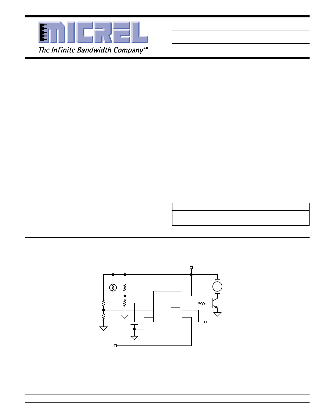
Typical Application
R3
R4
Secondary
Fan-control
Input
R2
12V
R1T1
C
F
1
2
3
4
MIC502
VT1
CF
VSLP
GND
VDD
OUT
OTF
VT2
8
R
BASE
7
6
5
Fan
Q1
Overtemperature
Fault Output
Micrel, Inc. • 1849 Fortune Drive • San Jose, CA 95131 • USA • tel + 1 (408) 944-0800 • fax + 1 (408) 944-0970 • http://www.micrel.com
August 2001 1 MIC502
Page 2
MIC502 Micrel
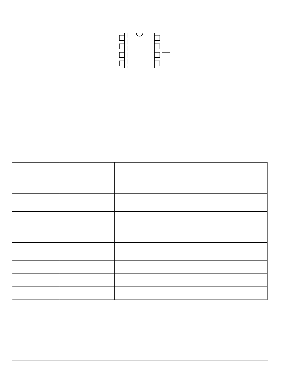
Pin Configuration
VT1
CF
VSLP
GND
Pin Description
Pin Number Pin Name Pin Function
1 VT1 Thermistor 1 (Input): Analog input of approximately 30% to 70% of V
2 CF PWM Timing Capacitor (External Component): Positive terminal for the
3 VSLP Sleep Threshold (Input): The voltage on this pin is compared to VT1 and VT2.
4 GND Ground
5 VT2 Thermistor 2 (Input): Analog input of approximately 30% to 70% of V
6 /OTF Overtemperature Fault (Output): Open-collector output (active low).
7 OUT Driver Output: Asymmetical-drive active-high complimentary PWM output.
8 VDD Power Supply (Input): IC supply input; may be independent of fan power
1
2
3
4
8
VDD
7
OUT
6
OTF
VT2
5
8-Pin SOIC (M)
8-Pin DIP (N)
produces active duty cycle of 0% to 100% at driver output (OUT). Connect to
external thermistor network (or other temperature sensor). Pull low for
shutdown.
PWM triangle-wave generator timing capacitor. The recommended CF is
0.1µF for 30Hz PWM operation.
When V
V
T2
disables the sleep-mode function.
< V
T1
SLP
rises above V
and VT2 < V
. (V
WAKE
WAKE
the MIC502 enters sleep mode until VT1 or
SLP
= V
SLP
+ V
.) Grounding VSLP
HYST
produces active duty cycle of 0% to 100% at driver output (OUT). Connect to
motherboard fan control signal or second temperature sensor.
Indicates overtemperature fault condition (VT1 > VOT) when active.
Typically connect to base of external NPN motor control transistor.
supply.
DD
DD
MIC502 2 August 2001
Page 3

MIC502 Micrel
Absolute Maximum Ratings (Note 1)
Supply Voltage (V
Output Sink Current (I
Output Source Current (I
Input Voltage (any pin) .........................–0.3V to VDD +0.3V
Junction Temperature (TJ) ...................................... +125°C
Storage Temperature (TA) ....................... –65°C to +150°C
Lead Temperature (Soldering, 5 sec.) ...................... 260°C
ESD, Note 3
) ..................................................+14V
DD
OUT(sink)
)..................................10mA
OUT(source)
) ..........................25mA
Operating Ratings (Note 2)
Supply Voltage (V
Sleep Voltage (V
Temperature Range (TA) ........................... –40°C to +85°C
Power Dissipation at 25°C
SOIC ...................................................................800mW
DIP ......................................................................740mW
Derating Factors
SOIC ...............................................................8.3mW/°C
Plastic DIP.......................................................7.7mW/°C
) ................................ +4.5V to +13.2V
DD
)........................................GND to V
SLP
DD
Electrical Characteristics
4.5V ≤ VDD ≤ 13.2V, Note 4; TA = 25, bold values indicate –40°C ≤ TA ≤ +85°C; unless noted
Symbol Parameter Condition Min Typ Max Units
I
DD
I
DD(slp)
Driver Output
t
R
t
F
I
OL
I
OH
I
OS
Thermistor and Sleep Inputs
V
PWM(max)
V
PWM(span)
V
HYST
V
IL
V
IH
V
OT
IVT, I
VSLP
t
RESET
Oscillator
f Oscillator Frequency, Note 7 4.5V ≤ VDD ≤ 5.5V, CF = 0.1µF 24 27 30 Hz
f
, f
MIN
MAX
t
STARTUP
Supply Current, Operating VSLP = grounded, OTF, OUT = open, 0.5 1.2 mA
CF = 0.1µF, VT1 = VT2 = 0.7 V
DD
Supply Current, Sleep VT1 = grounded, 240 400 µA
VSLP, OTF, OUT = open, CF = 0.1µF
Output Rise Time, Note 5 IOH = 10mA TBD 50 µs
Output Fall Time, Note 5 IOL = 1mA TBD 50 µs
Output Sink Current VOL = 0.5V 0.9 mA
Output Source Current 4.5V ≤ VDD ≤ 5.5V, VOH = 2.4V 10 mA
10.8V ≤ VDD ≤ 13.2V, VOH = 3.2V 10 mA
Sleep-Mode Output Leakage V
= 0V 1 µA
OUT
100% PWM Duty Cycle 67 70 73 %V
Input Voltage
V
PWM(max)
– V
PWM(min)
37 40 43 %V
Sleep Comparator Hysteresis 8 11 14 %V
VT1 Shutdown Threshold 0.7 V
VT1 Startup Threshold 1.1 V
VT1 Overtemperature Fault Note 6 74 77 80 %V
Threshold
VT1, VT2, VSLP Input Current –2.5 1 µA
Reset Setup Time minimum time VT1 < VIL, to guarantee reset, 30 µs
Note 5
10.8V ≤ VDD ≤ 13.2V, CF = 0.1µF 27 30 33 Hz
Oscillator Frequency Range Note 7 15 90 Hz
Startup Interval 64/f s
DD
DD
DD
DD
August 2001 3 MIC502
Page 4
MIC502 Micrel
Symbol Parameter Condition Min Typ Max Units
Overtemperature Fault Output
V
OL
I
OH
Note 1. Exceeding the absolute maximum rating may damage the device.
Note 2. The device is not guaranteed to function outside its operating rating.
Note 3. Devices are ESD sensitive. Handling precautions recommended.
Note 4: Part is functional over this VDD range; however, it is characterized for operation at 4.5V ≤ VDD ≤ 5.5V and 10.8V ≤ VDD ≤ 13.2V ranges. These
Note 5. Guaranteed by design.
Note 6. V
Note 7. Logic time base and PWM frequency. For other values of C
Active (Low) Output Voltage IOL = 2mA 0.3 V
Off-State Leakage V
ranges correspond to nominal V
is guaranteed by design to always be higher than V
OT
of 5V and 12V, respectively.
DD
/OTF
PWM(max)
= V
DD
,
f(Hz) = 30Hz
F
1 µA
.
0.1 FCµ
, where C is in µF.
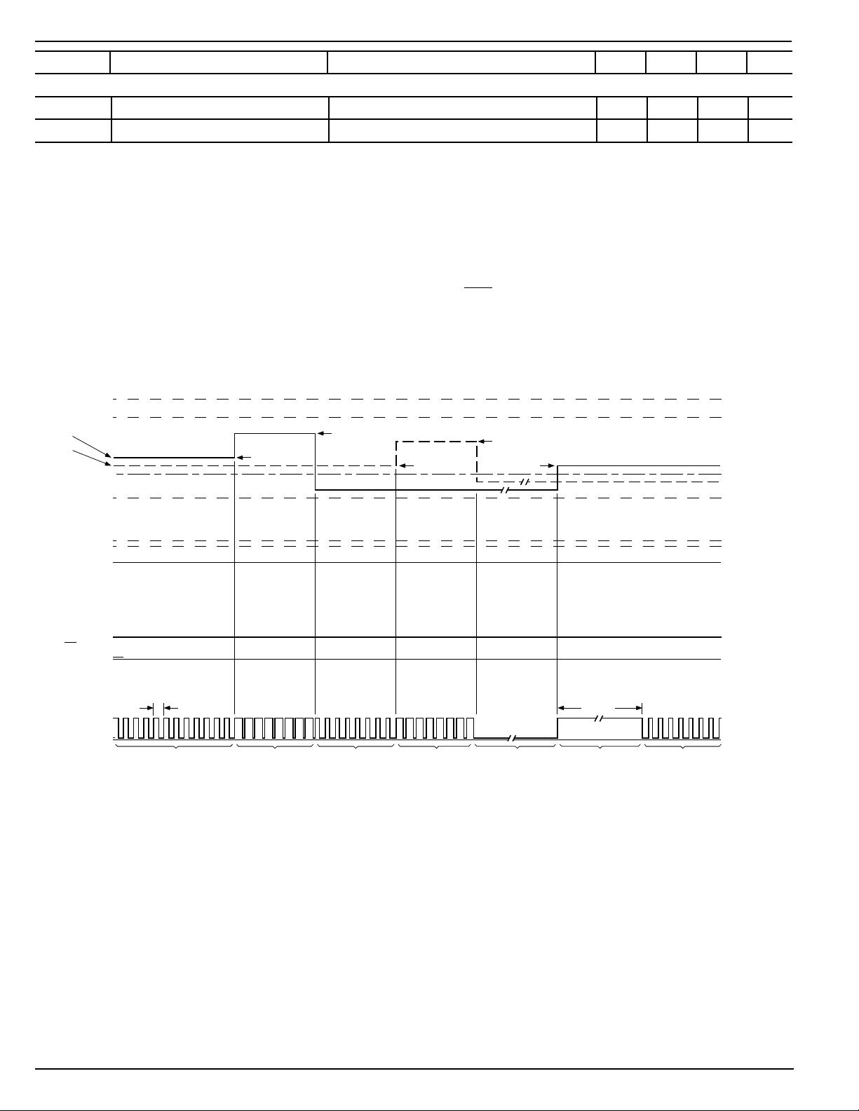
Timing Diagrams
V
OT
0.7V
DD
V
T1
V
T2
V
SLP
0.3VDD0.3V
DD
50%
80%
40%
70%
40%
100%
Input
Signal
Range
30%
0%
V
IH
V
IL
0V
V
OH
V
OTF
V
OL
0V
50%
t
PWM
80% 40% 0% 100% 40%70%
ABCDE
V
OH
V
OUT
V
OL
0V
Figure 1. Typical System Behavior
Note A. Output duty-cycle is initially determined by VT1, as it is greater than VT2.
Note B. PWM duty-cycle follows VT1 as it increases.
Note C. VT1 drops below VT2. VT2 now determines the output duty-cycle.
Note D. The PWM duty-cycle follows VT2 as it increases.
Note E. Both VT1 and VT2 decrease below V
Note F. The PWM ‘wakes up’ because one of the control inputs (VT1 in this case) has risen above V
high for 64 clock periods. (V
WAKE
Note G. Following the startup interval, the PWM duty-cycle is the higher of VT1 and VT2.
but above VIL. The device enters sleep mode.
SLP
= V
SLP
+ V
. See “Electrical Characteristics.”)
HYST
F
t
STARTUP
. The startup timer is triggered, forcing OUT
WAKE
G
Output
Duty Cycle
MIC502 4 August 2001
Page 5
MIC502 Micrel
V
OT
0.7V
DD
V
T1
V
T2
V
SLP
0.3VDD0.3V
DD
V
IH
V
IL
40%
60%
30%
0V
100%
PWM
Range
20%
0%
V
OH
V
OTF
V
OL
0V
HI
t
V
OH
V
OUT
V
OL
0V
V
DD
V
DD
STARTUP
100%
40%
t
PWM
JK
60% 30% 0%100%
L
M
N
O
0V
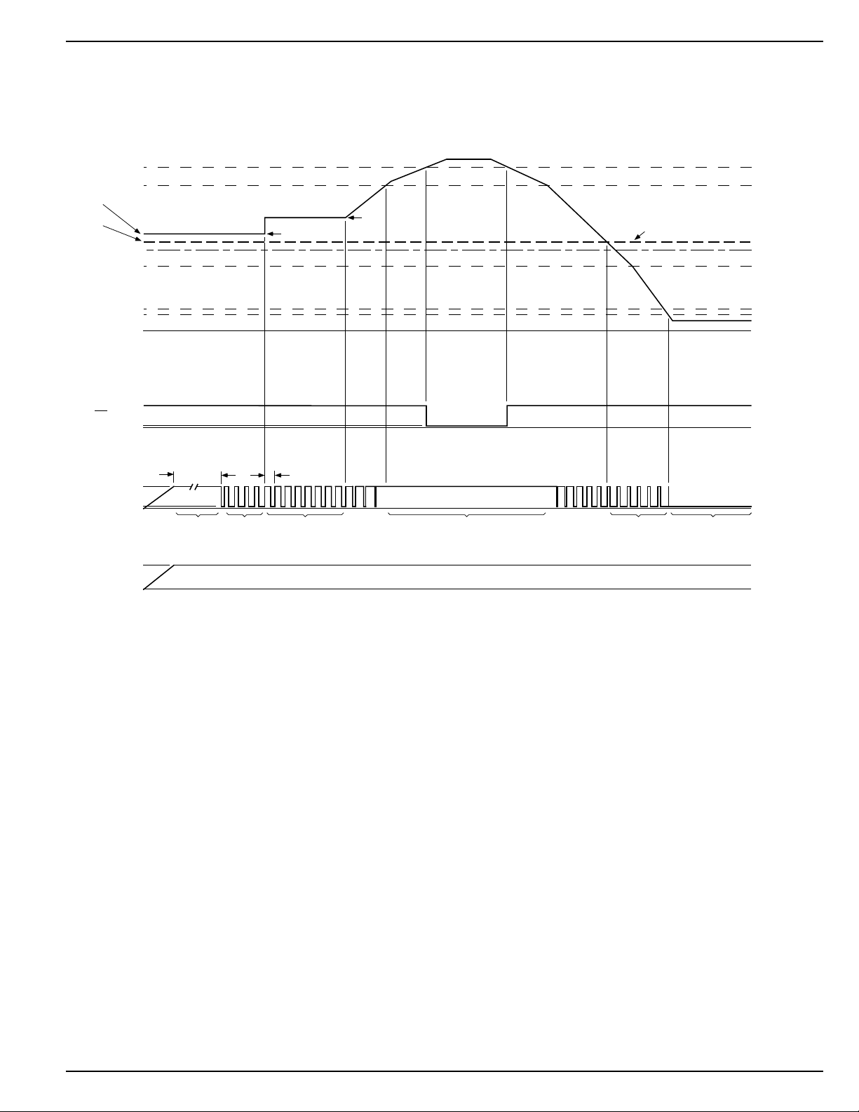
Figure 2. MIC502 Typical Power-Up System Behavior
Note H. At power-on, the startup timer forces OUT on for 64 PWM cycles of the internal timebase (t
dead stop.
Note I. The PWM duty-cycle follows the higher of VT1 and V
in the case, VT1.
T2,
Note J. The PWM duty-cycle follows VT1 as it increases.
Note K. PWM duty-cycle is 100% (OUT constantly on) anytime VT1 > V
PWM(max)
.
Note L. /OTF is asserted anytime VT1 > VOT. (The fan continues to run at 100% duty-cycle.)
Note M. /OTF is deasserted when VT1 falls below VOT; duty-cycle once again follows VT1.
Note N. Duty-cycle follows VT1 until VT1 < VT2, at which time VT2 becomes the controlling input signal. Note that VT1 is below V
normal operation continues. (Both VT1 and VT2 must be below V
to active sleep mode.)
SLP
Note O. All functions cease when VT1 < VIL; this occurs regardless of the state of VT2.
). This insures that the fan will start from a
PWM
Output
Duty Cycle
but above VIH; so
SLP
August 2001 5 MIC502
Page 6
MIC502 Micrel
g
g
g
y
g
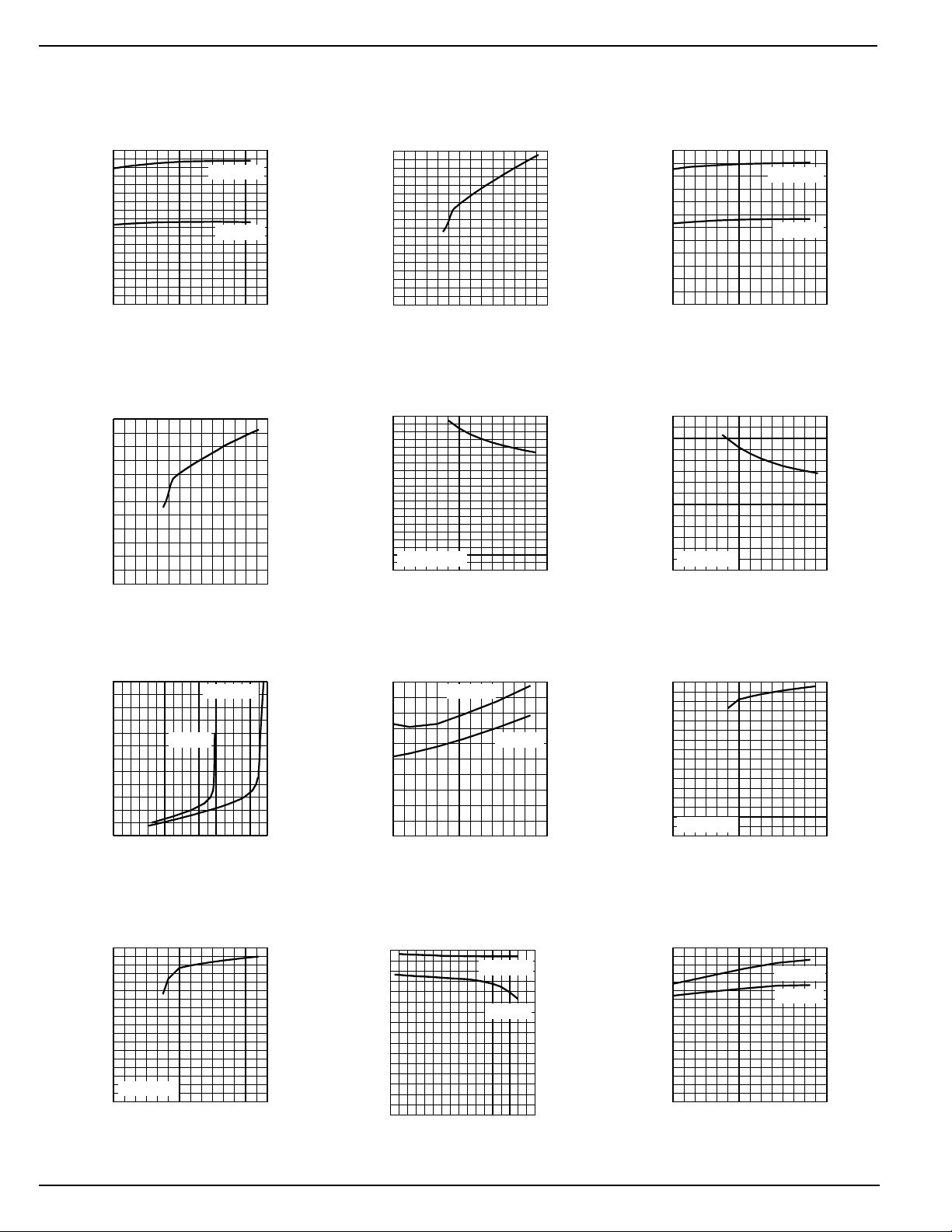
Typical Characteristics
Supply Current
vs. Temperature
0.9
0.8
0.7
0.6
0.5
(mA)
0.4
DD
I
0.3
0.2
0.1
0
-40 -20 0 20 40 60 80 100
TEMPERATURE (°C)
IDD
0.3
Suppl
SLEEP
Voltage
VDD = 12V
VDD = 5V
vs.
0.25
0.2
(mA)
0.15
SLEEP
0.1
IDD
0.05
0
02468101214
VDD (V)
Supply Current
vs. Supply Voltage
0.9
0.8
0.7
0.6
0.5
(mA)
0.4
DD
I
0.3
0.2
0.1
0
02468101214
VDD (V)
VOLvs.
Supply Volta
IOL = 0.9mA
0
02468101214
VDD (V)
(V)
V
0.20
0.18
0.16
0.14
0.12
0.10
OL
0.08
0.06
0.04
0.02
IDD
Temperature
0
-40 -20 0 20 40 60 80 100
TEMPERATURE (°C)
0.25
(mA)
0.15
SLEEP
IDD
0.05
0.3
0.2
0.1
SLEEP
vs.
VDD = 12V
VDD = 5V
VOLvs.
e
(mV)
OL
V
Supply Volta
35
30
25
20
15
10
5
IOL = 100µA
0
02468101214
VDD (V)
e
VOL vs. I
1.2
1
0.8
(V)
0.6
OL
V
0.4
0.2
0
0 0.2 0.4 0.6 0.8 1 1.2 1.4 1.6 1.8
OL
VDD =12V
VDD =5V
IOL (mA)
VOHvs.
Supply Volta
4
3
2
1
IOH = 100µA
0
02468101214
VDD (V)
(V)
V
4.5
3.5
2.5
OH
1.5
0.5
e
V
OL
vs. Temperature
VDD = 5V
VDD =12V
0
-40 -20 0 20 40 60 80 100
TEMPERATURE (°C)
VOH vs. I
OH
(V)
V
0.25
0.20
0.15
OL
0.10
0.05
4
3.5
VDD =12V
3
VDD =5V
(V)
V
2.5
2
OH
1.5
1
0.5
0
35791113151719
IOH (mA)
VOHvs.
Supply Volta
4
3.5
3
2.5
(V)
2
OH
V
1.5
1
0.5
IOH = 10mA
0
02468101214
VDD (V)
e
VOHvs.
Temperature
4
3
2
1
0
-40 -20 0 20 40 60 80 100
TEMPERATURE (°C)
VDD = 12V
VDD = 5V
(V)
V
4.5
3.5
2.5
OH
1.5
0.5
MIC502 6 August 2001
Page 7
MIC502 Micrel
g
1
10
100
1000
3000
0.001 0.01 0.1 1
FREQUENCY (Hz)
CAPACITANCE (µF)
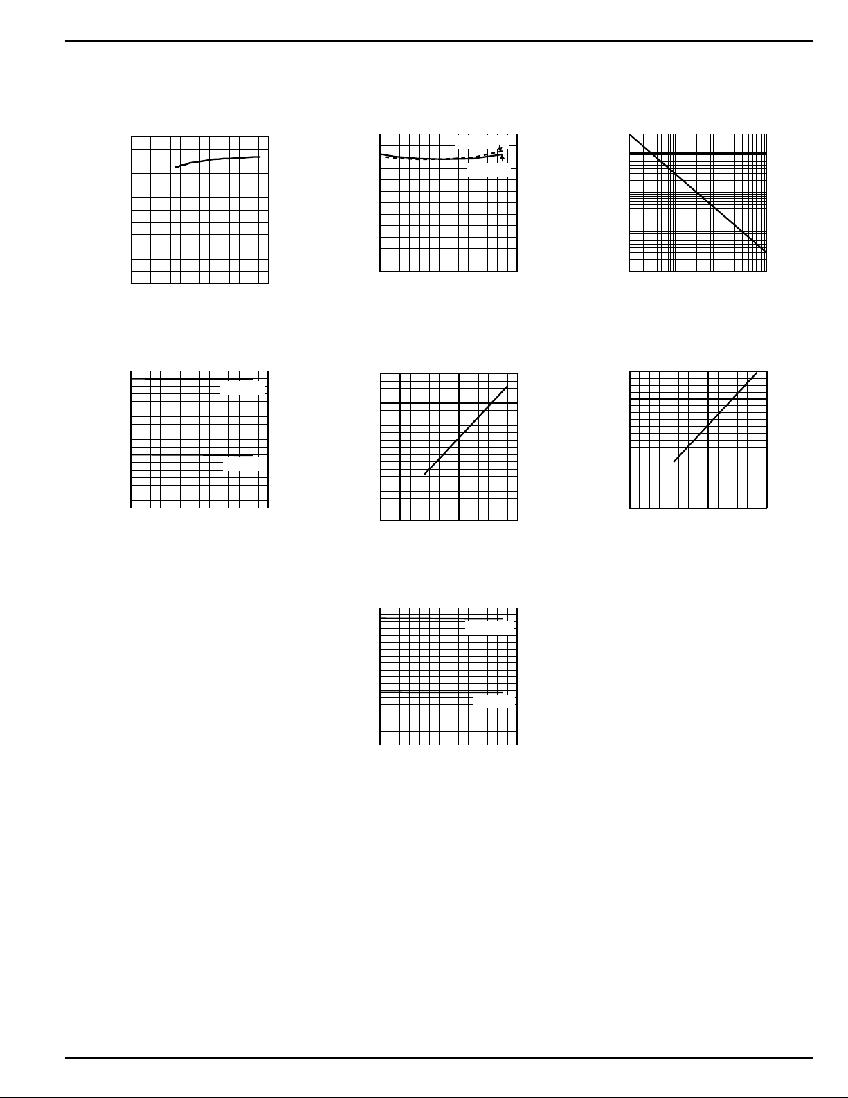
PWM Frequency vs.
Timing Capacitor Value
PWM Frequency(Normalized)
vs. Supply Volta
1.2
1
0.8
0.6
(NORMALIZED)
0.4
PWM
F
0.2
0
02468101214
9
8
7
6
(V)
5
4
PWM(MAX)
3
V
2
1
0
-40 -20 0 20 40 60 80 100
VDD (V)
V
PWM(max)
vs. Temperature
TEMPERATURE (°C)
e
VDD =12V
VDD = 5V
PWM Frequency (normalized)
vs. Temperature
1.2
1
0.8
0.6
(NORMALIZED)
0.4
PWM
F
0.2
0
-40 -20 0 20 40 60 80 100
TEMPERATURE (°C)
10
Supply Voltage
V
PWM(max)
VDD = 12V
VDD = 5V
vs.
9
8
7
6
(V)
5
PWM
4
V
3
2
1
0
02468101214
VDD (V)
VOTvs.
Supply Voltage
9
8
7
6
5
4
3
2
1
0
02468101214
VDD (V)
(V)
OT
V
10
V
OT
vs. Temperature
10
9
8
7
6
(V)
5
OT
V
4
3
2
1
0
-40 -20 0 20 40 60 80 100
TEMPERATURE (°C)
VDD = 12V
VDD = 5V
August 2001 7 MIC502
Page 8
MIC502 Micrel
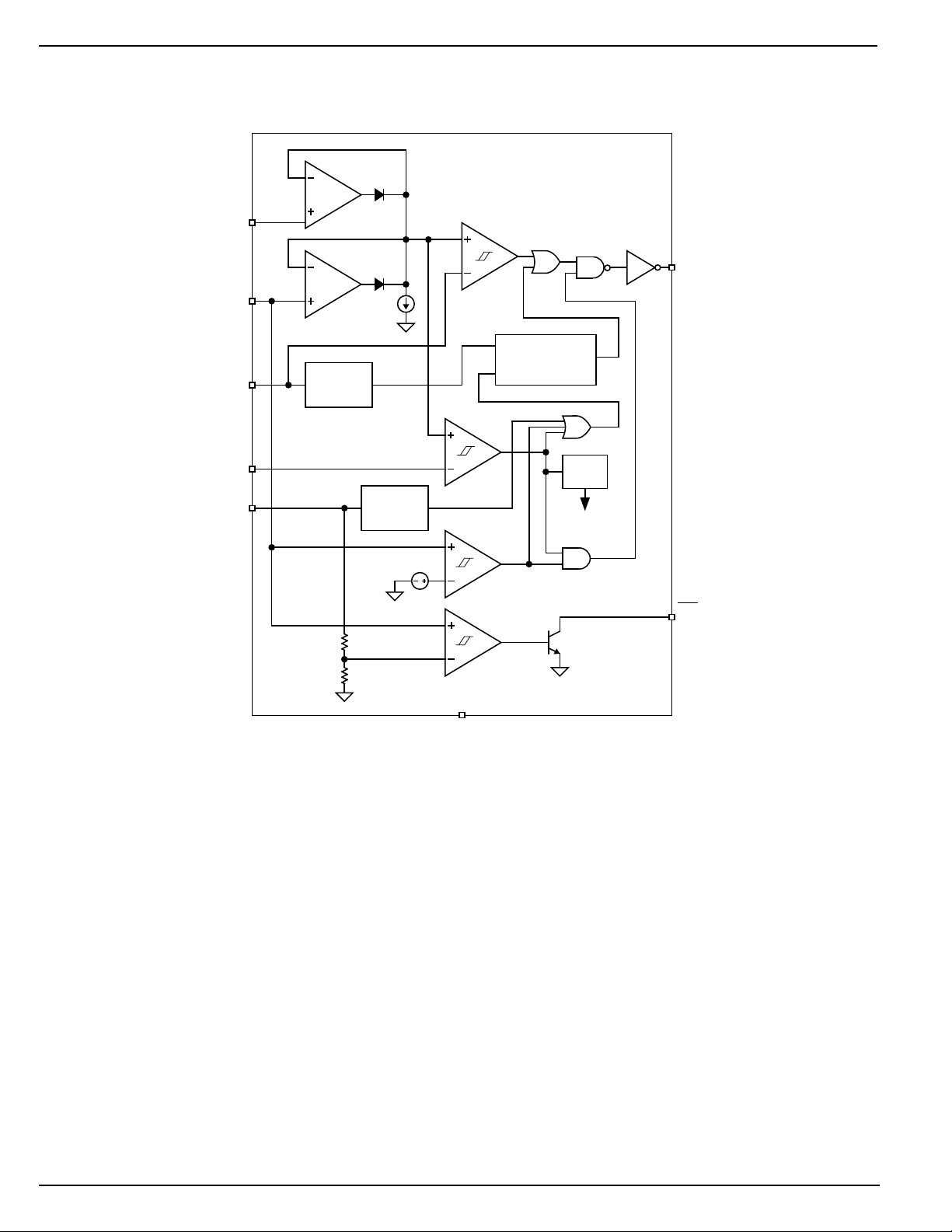
Functional Diagram
VT2
VT1
CF
VSLP
VDD
5
PWM
Driver
OUT
7
1
CLK
Start-Up
OUT
Timer
2
Oscillator
RESET
Sleep
Sleep
3
Power-On
8
Reset
Control
Bias
Reset
V
IL
Overtemperature
ENABLE
OTF
6
4
GND
MIC502 8 August 2001
Page 9
MIC502 Micrel
Functional Description
Oscillator
A capacitor connected to CF determines the frequency of the
internal time base which drives the state-machine logic and
determines the PWM frequency. This operating frequency
will be typically 30Hz to 60Hz. (CF = 0.1µF for 30Hz.)
Pulse-Width Modulator
A triangle-wave generator and threshold detector comprise
the internal pulse-width modulator (PWM). The PWM’s output duty-cycle is determined by the higher of VT1 or VT2. A
typical voltage range of 30% to 70% of VDD applied to the VT1
and VT2 pins corresponds to 0% to 100% duty-cycle. Since
at least one of the control voltage inputs is generally from a
thermistor-resistor divider connected to VDD, the PWM output duty cycle will not be affected by changes in the supply
voltage.
Driver Output
OUT is a complementary push-pull digital output with asymmetric drive (approximately 10mA source, 1mA sink—see
“Electrical Characteristics”). It is optimized for directly driving
an NPN transistor switch in the fan’s ground-return. See
“Applications Information” for circuit details.
Shutdown/Reset
Internal circuitry automatically performs a reset of the MIC502
when power is applied. The MIC502 may be shut down at any
time by forcing VT1 below its VIL threshold. This is typically
accomplished by connecting the VT1 pin to open-drain or
open-collector logic and results in an immediate and asynchronous shutdown of the MIC502. The OUT and /OTF pins
will float while VT1 is below VIL.
If VT1 then rises above VIH, a device reset occurs. Reset is
equivalent to a power-up condition: the state of /OTF is
cleared, a startup interval is triggered, and normal fan operation begins.
Startup Interval
Any time the fan is started from the off state (power-on or
coming out of sleep mode or shutdown mode), the PWM
output is automatically forced high for a startup interval of 64
× t
. Once the startup interval is complete, PWM operation
PWM
will commence and the duty-cycle of the output will be
determined by the higher of VT1 or VT2.
Overtemperature Fault Output
/OTF is an active-low, open-collector logic output. An overtemperature condition will cause /OTF to be asserted. An
overtemperature condition is determined by VT1 exceeding
the normal operating range of 30% to 70% of VDD by > 7% of
VDD. Note that VOT is guaranteed by design to always be
higher than V
PWM(max)
Sleep Mode
When VT1 and VT2 fall below V
capable of operating without fan cooling and the MIC502
enters sleep mode and discontinues fan operation. The
threshold where the MIC502 enters sleep mode is determined by V
. Connecting the VSLP pin to ground disables
SLP
sleep mode.
.
, the system is deemed
SLP
Once in sleep mode, all device functions cease (/OTF inactive, PWM output off) unless VT1 or VT2 rise above V
(V
WAKE
= V
SLP
+ V
HYST
.) V
is a fixed amount of hyster-
HYST
WAKE
esis added to the sleep comparator which prevents erratic
operation around the V
operating point. The result is
SLP
stable and predictable thermostatic action: whenever possible the fan is shut down to reduce energy consumption and
acoustic noise, but will always be activated if the system
temperature rises.
If the device powers-up or exits its reset state, the fan will not
start unless VT1 or VT2 rises above V
WAKE
.
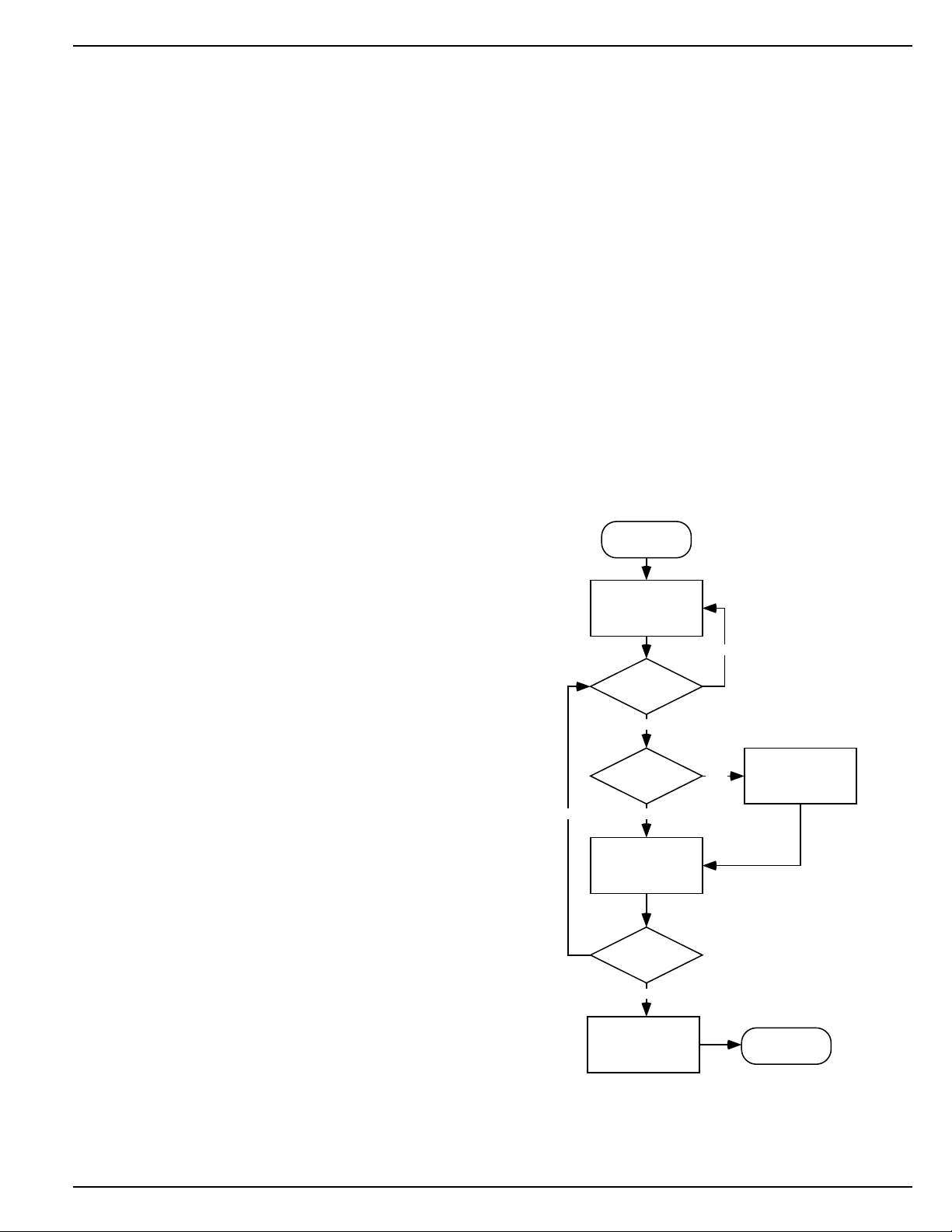
System Operation
Power Up
• A complete reset occurs when power is applied.
• OUT is off (low) and /OTF is inactive (high/floating).
• If VT1 < VIL, the MIC502 remains in shutdown.
• The startup interval begins. OUT will be on (high) for 64
clock cycles (64 × t
PWM
).
• Following the startup interval, normal operation begins.
POWER ON
Reset Startup Timer;
Deassert /OTF;
OUT Off (Low).
YES
VT1 < V
IL
?
NO
NO
OUT Held On (High)
VT1 > V
OT
?
NO
During Startup
Interval.
Startup Interval
Finished
?
YES
Deassert OUT
(OUT = Low)
YES
Assert /OTF While
V
> V
T1
OT
NORMAL
OPERATION
Figure 3. Power-Up Behavior
.
August 2001 9 MIC502
Page 10
MIC502 Micrel
Normal Operation
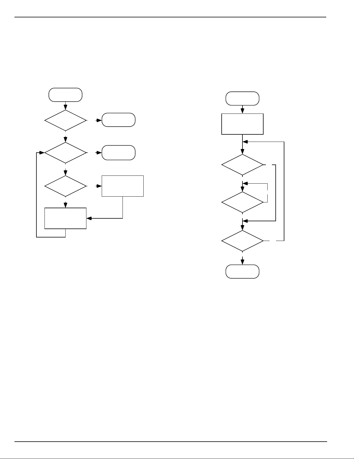
Normal operation consists of the PWM operating to control
the speed of the fan according to VT1 and VT2. Exceptions to
this otherwise indefinite behavior can be caused by any of
three conditions: VT1 exceeding VOT, an overtemperature
condition; VT1 being pulled below VIL initiating a device
shutdown and reset; or both VT1 and VT2 falling below V
SLP
activating sleep mode. Each of these exceptions is treated as
follows:
NORMAL
OPERATION
Reset?
V
< V
T1
IL
?
NO
VT1 and V
< V
SLEEP
?
NO
Overtemp?
V
> V
T1
OT
?
NO
OUT Duty Cycle
Proportional to
Greater of V
T1
YES
T2
YES
YES
, V
T2
POWER ON
SLEEP
Assert /OTF while
V
> V
T1
OT
Sleep Mode
During normal operation, if VT1 and VT2 fall below V
device will go into sleep mode and fan operation will stop. The
MIC502 will exit sleep mode when VT1 or VT2 rise above V
by the hysteresis voltage, V
. When this occurs, normal
HYST
operation will resume. The resumption of normal operation
,
upon exiting sleep is indistinguishable from a power-on reset.
(See “Sleep: Normal Operation,” above.)
SLEEP
Disable PWM
Reset Initiated
V
< V
T1
IL
?
YES
Reset Released
V
> V
T1
IH
?
YES
NO
NO
SLP
, the
SLP
Figure 4. Normal System Behavior
•
Overtemperature:
If the system temperature rises
typically 7% above the 100% duty-cycle operating point,
/OTF will be activated to indicate an overtemperature
fault. (VT1 > VOT) Overtemperature detection is essentially independent of other operations—the PWM
continues its normal behavior; with VT1 > V
PWM(max)
output duty-cycle will be 100%. If VT1 falls below VOT,
the overtemperature condition is cleared and /OTF is no
longer asserted. It is assumed that in most systems, the
/OTF output will initiate power supply shutdown.
•
Shutdown/Reset:
If VT1 is driven below VIL an immediate, asynchronous shutdown occurs. While in shutdown
mode, OUT is off (low), and /OTF is unconditionally
inactive (high/floating). If VT1 subsequently rises above
VIH, a device reset will occur. Reset is indistinguishable
from a power-up condition. The state of /OTF is cleared,
a startup interval is triggered, and normal fan operation
begins.
•
Sleep:
If VT1 and VT2 fall below V
, the device enters
SLP
sleep mode. All internal functions cease unless VT1 or
VT2 rise above V
WAKE
. (V
WAKE
= V
SLP
+ V
HYST
.) The
/OTF output is unconditionally inactive (high/floating)
and the PWM is disabled during sleep. (OUT will float.)
, the
Wake Up?
V
or VT2 >
T1
V
SLP+VHYST
?
YES
POWER ON
NO
Figure 5. Sleep-Mode Behavior
MIC502 10 August 2001
Page 11

MIC502 Micrel
Applications Information
The Typical Application drawing on page 1 illustrates a typical
application circuit for the MIC502. Interfacing the MIC502
with a system consists of the following steps:
1. Selecting a temperature sensor
2. Interfacing the temperature sensor to the VT1 input
3 Selecting a fan-drive transistor, and base-drive current
limit resistor
4. Deciding what to do with the Secondary
Fan-Control Input
5. Making use of the Overtemperature Fault Output.
Temperature Sensor Selection
Temperature sensor T1 is a negative temperature coefficient
(NTC) thermistor. The MIC502 can be interfaced with either
a negative or positive tempco thermistor; however, a negative temperature coefficient thermistor typically costs less
than its equivalent positive tempco counterpart. While a
variety of thermistors can be used in this application, the
following paragraphs reveal that those with an R25 rating
(resistance at 25°C) of from about 50kΩ to 100kΩ lend
themselves nicely to an interface network that requires only
a modest current drain. Keeping the thermistor bias current
low not only indicates prudent design; it also prevents selfheating of the sensor from becoming an additional design
consideration. It is assumed that the thermistor will be located
within the system power supply, which most likely also
houses the speed-controlled fan.
Temperature Sensor Interface
As shown by the Electrical Characteristics table, the working
voltage for input VT1 is specified as a percentage of VDD. This
conveniently frees the designer from having to be concerned
with interactions resulting from variations in the supply voltage. By design, the operating range of VT1 is from about 30%
of VDD to about 70% of VDD.
V
PWM(min)
When VT1 = V
drive signal is generated. Conversely, when VT1 = V
≈ 0.3VDD, the motor-drive signal has a 0% duty cycle.
Resistor voltage divider R1 || T1, R2 in the Typical Application
diagram is designed to preset VT1 to a value of V
corresponds to the slowest desired fan speed when the
resistance of thermistor T1 is at its highest (cold) value. As
temperature rises the resistance of T1 decreases and V
increases because of the parallel connection of R1 and T1.
Since VT1 = V
cycle drive), and since it is foreseen that at least some cooling
will almost always be required, the lowest voltage applied to
the VT1 input will normally be somewhat higher than 0.3V
(or >V
PWM(min)
mode rather than operate the fan at a very low duty cycle
(<< 25%). Operation at very low duty cycle results in relatively
little airflow. Sleep mode should be used to reduce acoustic
noise when the system is cool. For a given minimum desired
fan speed, a corresponding V
the following observation:
= V
PWM(max)
PWM(max)
PWM(min)
– V
PWM(span)
≈ 0.7VDD, a 100% duty-cycle motor
PWM(min)
that
PWM
represents a stopped fan (0% duty-
DD
). It is assumed that the system will be in sleep
can be determined via
T1(min)
T1
since
V
PWM(max)
= 70% of VDD ∝ 100% RPM
and
V
PWM(min)
= 30% of VDD ∝ 0% RPM
then
V
PWM(span)
= 40% of VDD ∝ 100% RPM
range
.
Figure 6 shows the following linear relationship between the
voltage applied to the VT1 input, motor drive duty cycle, and
approximate
motor speed.
since
VT1 = 0.7VDD ∝ 100% PWM
then
VT1 = 0.6VDD ∝ 75% PWM
and
VT1 = 0.5VDD ∝ 50% PWM
and
VT1 = 0.4VDD ∝ 25% PWM.
In addition to the R25 thermistor rating, sometimes a data
sheet will provide the ratio of R25/R50 (resistance at 25°C
divided by resistance at 50°C) is given. Sometimes this is
given as an R0/R50 ratio. Other data sheet contents either
specify or help the user determine device resistance at
arbitrary temperatures. The thermistor interface to the MIC502
usually consists of the thermistor and two resistors.
100
80
60
40
DUTY CYCLE (%)
20
0
0 20406080100
VT1/SUPPLY VOLTAGE (%)
Figure 6. Control Voltage vs. Fan Speed
Design Example
The thermistor-resistor interface network is shown in the
Typical Application drawing. The following example describes
the design process: A thermistor data sheet specifies a
thermistor that is a candidate for this design as having an R25
resistance of 100kΩ. The data sheet also supports calculation of resistance at arbitrary temperatures, and it was discovered the candidate thermistor has a resistance of 13.6k at
70°C (R70). Accuracy is more important at the higher temperature end of the operating range (70°C) than the lower end
because we wish the overtemperature fault output (/OTF) to
be reasonably accurate—it may be critical to operating a
power supply crowbar or other shutdown mechanism, for
example. The lower temperature end of the range is less
important because it simply establishes minimum fan speed,
which is when less cooling is required.
August 2001 11 MIC502
Page 12

MIC502 Micrel
Referring to the “Typical Application,” the following approach
can be used to design the required thermistor interface
network:
Let
R1 = ∞
RT1 = 13.6k (at 70°C)
and
VT = 0.7V
Since
V=
T
0.7=
0.7RT1 + 0.7R2 = R2
0.7RT1 = 0.3R2
and
R2 = 2.33RT1 = 2.33 × 13.6k = 31.7k ≈ 33k
Let’s continue by determining what the temperature-proportional voltage is at 25°C.
Let
R1 = ∞
and
RT1 = 100k (at 25°C).
From
V=
T
V=
T
VT = 0.248V
Recalling from above discussion that the desired VT for 25°C
should be about 40% of VDD, the above value of 24.8% is far
too low. This would produce a voltage that would stop the fan
(recall from the above that this occurs when VT is about 30%
of VDD. To choose an appropriate value for R1 we need to
learn what the parallel combination of RT1 and R1 should be
at 25°C:
Again
V=
T
0.4=
0.4(RT1 || R1) + 0.4R2 = R2
0.4(RT1 || R1) = 0.6R2
and
RT1 || R1 = 1.5R2 = 1.5 × 33k = 49.5k
Since
DD
VR2
DD
R||R1+R2
()
T1
R2
R+R2
()
T1
VR2
×
DD
R+R2
()
T1
V 33k
×
DD
100k+33k
()
VR2
DD
R||R1+R2
()
T1
R2
R||R1+R2
()
T1
(70% of VDD)
×
DD
×
RT1 = 100k
and
RT1 || R1 = 49.5k ≈ 50k
let
R1 = 100k
While that solves the low temperature end of the range, there
is a small effect on the other end of the scale. The new value
of VT for 70°C is 0.734, or about 73% of VDD. This represents
only a 3% shift from the design goal of 70% of VDD. In
summary, R1 = 100k, and R2 = 33k. The candidate thermistor
used in this design example is the RL2010-54.1K-138-D1,
manufactured by Keystone Thermometrics.
The R25 resistance (100kΩ) of the chosen thermistor is
probably on the high side of the range of potential thermistor
resistances. The result is a moderately high-impedance
network for connecting to the VT1 and/or VT2 input(s). Because these inputs can have up to 1µA of leakage current,
care must be taken if the input network impedance becomes
higher than the example. Leakage current and resistor accuracy could require consideration in such designs. Note that
the V
Secondary Fan-Control Input
The above discussions also apply to the secondary fancontrol input, VT2, pin 5. It is possible that a second thermistor, mounted at another temperature-critical location outside the power supply, may be appropriate. There is also the
possibility of accommodating the NLX “FanC” signal via this
input. If a second thermistor is the desired solution, the VT2
input may be treated exactly like the VT1 input. The above
discussions then apply directly. If, however, the NLX FanC
signal is to be incorporated into the design then the operating
voltage (VDD = 5V vs. VDD = 12V) becomes a concern. The
FanC signal is derived from a 12V supply and is specified to
swing at least to 10.5V. A minimum implementation of the
FanC signal would provide the capability of asserting fullspeed operation of the fan; this is the case when 10.5V ≤
FanC ≤ 12V. This FanC signal can be applied directly to the
VT2 input of the MIC502, but only when its VDD is 12V. If this
signal is required when the MIC502 VDD = 5V a resistor
divider is necessary to reduce this input voltage so it does not
exceed the MIC502 VDD voltage. A good number is 4V
(80%VDD).
Because of input leakage considerations, the impedance of
the resistive divider should be kept at ≤ 100kΩ. A series
resistor of 120kΩ driven by the Fan C signal and a 100kΩ
shunt resistor to ground make a good divider for driving the
VT2 input.
Transistor and Base-Drive Resistor Selection
The OUT motor-drive output, pin 7, is intended for driving a
medium-power device, such as an NPN transistor. A rather
ubiquitous transistor, the 2N2222A, is capable of switching
up to about 400mA. It is also available as the PN2222A in a
plastic TO-92 package. Since 400mA is about the maximum
current for most popular computer power supply fans (with
many drawing substantially less current) and since the MIC502
provides a minimum of 10mA output current, the PN2222A,
with its minimum β of 40, is the chosen motor-drive transistor.
input has this same leakage current specification.
SLP
MIC502 12 August 2001
Page 13
MIC502 Micrel
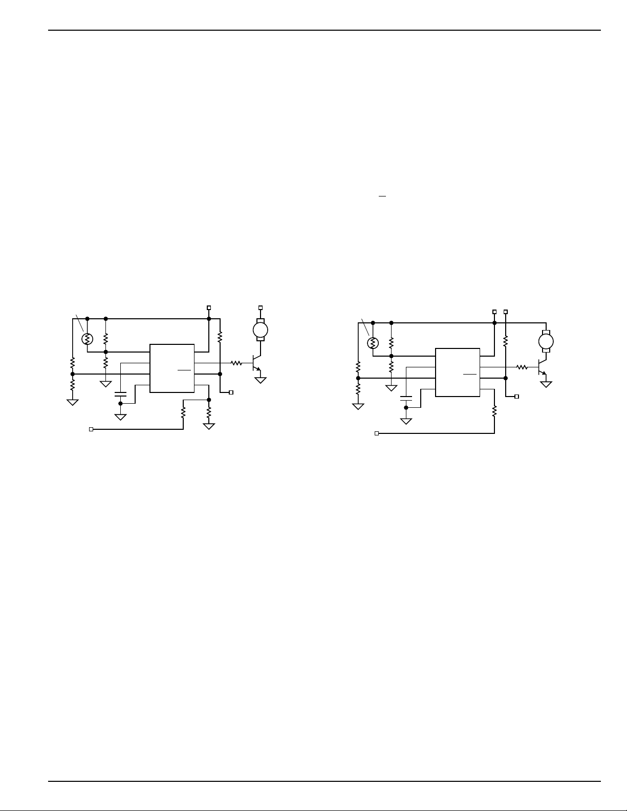
The design consists soley of choosing the value R
BASE
in
Figures 7 and 8. To minimize on-chip power dissipation in the
MIC502, the value of R
should be determined by the
BASE
power supply voltage. The Electrical Characteristics table
specifies a minimum output current of 10mA. However,
different output voltage drops (VDD – V
12V operation. The value R
should be as high as
BASE
) exist for 5V vs.
OUT
possible for a given required transistor base-drive current in
order to reduce on-chip power dissipation.
Referring to the “Typical Application” and to the “Electrical
Characteristics” table, the value for R
is calculated as
BASE
follows. For VDD = 5V systems, IOH of OUT (pin 7) is
guaranteed to be a minimum of 10mA with a VOH of 2.4V.
R
then equals (2.4V – VBE) ÷ 10mA = 170Ω.
BASE
For VDD = 12V systems, R
= (3.4 – 0.7) ÷ 0.01 = 250Ω.
BASE
Overtemperature Fault Output
The /OTF output, pin 6, is an open-collector NPN output. It is
compatible with CMOS and TTL logic and is intended for
Keystone Thermonics
RL2010-54.1K-138-D1
or similar
R1
T1
100k
R2
R3
33k
56k
R4
56k
C
F
0.1µF
NLX FanC
Signal Input
1
2
3
4
MIC502
VT1
CF
VSLP
GND
VDD
OUT
OTF
VT2
120k
5V
47k
8
7
6
5
100k
12V
R
BASE
180Ω
Q1
Overtemperature
Fault Output
Yate Loon
YD80SM-12
or similar fan
alerting a system about an overtemperature condition or
triggering a power supply crowbar circuit. If VDD for the
MIC502 is 5V the output should not be pulled to a higher
voltage. This output can sink up to 2mA and remain compatible with the TTL logic-low level.
Timing Capacitors vs. PWM Frequency
The recommended CF (see first page) is 0.1µF for opertaion
at a PWM frequency of 30Hz. This frequency is factory
trimmed within ±3Hz using a 0.1% accurate capacitor. If it is
desired to operate at a different frequency, the new value for
CF is calculated as follows:
3
C=
, where C is in µF and f is in Hz.
f
The composition, voltage rating, ESR, etc., parameters of the
capacitor are not critical. However, if tight control of frequency
vs. temperature is an issue, the temperature coefficient may
become a consideration.
Keystone Thermonics
RL2010-54.1K-138-D1
or similar
R1
T1
100k
R2
R3
33k
56k
R4
56k
C
F
0.1µF
NLX FanC
Signal Input
1
2
3
4
MIC502
VT1
CF
VSLP
GND
VDD
OUT
OTF
VT2
8
7
6
5
12V
5V
47k
R
BASE
280Ω
Overtemperature
Fault Output
4.7k
Yate Loon
YD80SM-12
or similar fan
Q1
Figure 7. Typical 5V VDD Application Circuit
Figure 8. Typical 12V VDD Application Circuit
August 2001 13 MIC502
Page 14
MIC502 Micrel
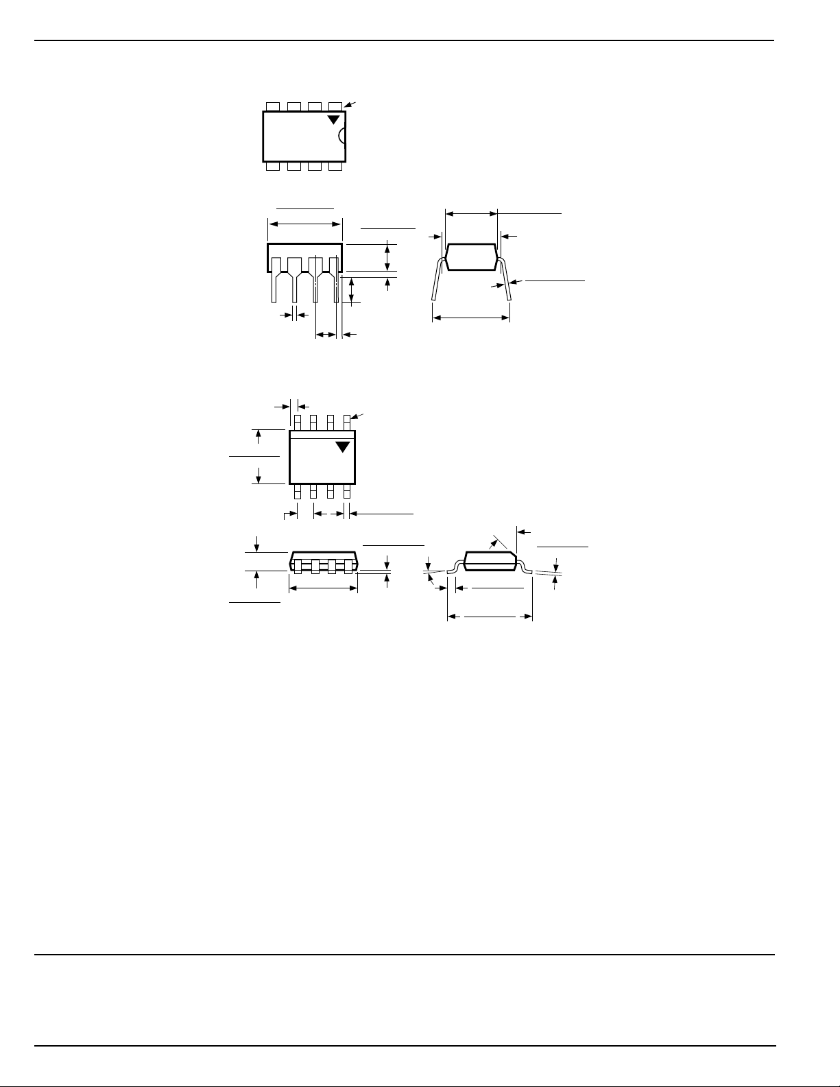
Package Information
PIN 1
DIMENSIONS:
INCH (MM)
0.018 (0.57)
0.100 (2.54)
0.026 (0.65)
MAX)
0.157 (3.99)
0.150 (3.81)
0.050 (1.27)
0.064 (1.63)
0.045 (1.14)
0.380 (9.65)
0.370 (9.40)
TYP
0.197 (5.0)
0.189 (4.8)
0.135 (3.43)
0.125 (3.18)
0.130 (3.30)
0.0375 (0.952)
0.380 (9.65)
0.320 (8.13)
8-Pin Plastic DIP (N)
PIN 1
DIMENSIONS:
INCHES (MM)
0.020 (0.51)
0.013 (0.33)
0.0098 (0.249)
0.0040 (0.102)
0°–8°
SEATING
PLANE
45°
0.050 (1.27)
0.016 (0.40)
0.244 (6.20)
0.228 (5.79)
0.255 (6.48)
0.245 (6.22)
0.300 (7.62)
0.013 (0.330)
0.010 (0.254)
0.010 (0.25)
0.007 (0.18)
8-Pin SOP (M)
MICREL INC. 1849 FORTUNE DRIVE SAN JOSE, CA 95131 USA
TEL + 1 (408) 944-0800 FAX + 1 (408) 944-0970 WEB http://www.micrel.com
This information is believed to be accurate and reliable, however no responsibility is assumed by Micrel for its use nor for any infringement of patents or
other rights of third parties resulting from its use. No license is granted by implication or otherwise under any patent or patent right of Micrel Inc.
© 2001 Micrel Incorporated
MIC502 14 August 2001
Page 15

This datasheet has been download from:
www.datasheetcatalog.com
Datasheets for electronics components.
 Loading...