

MICREL MIC5018 Datasheet
MIC5018 Micrel
MIC5018
IttyBitty™ High-Side MOSFET Driver
Preliminary Information
General Description
The MIC5018 IttyBitty™ high-side MOSFET driver is designed to switch an N-channel enhancement-type MOSFET
from a TTL compatible control signal in high- or low-side
switch applications. This driver features the tiny 4-lead
SOT-143 package.
The MIC5018 is powered from a +2.7V to +9V supply and
features extremely low off-state supply current. An internal
charge pump drives the gate output higher than the driver
supply voltage and can sustain the gate voltage indefinitely.
An internal zener diode limits the gate-to-source voltage to a
safe level for standard N-channel MOSFETs.
In high-side configurations, the source voltage of the MOSFET approaches the supply voltage when switched on. To
keep the MOSFET turned on, the MIC5018’s output drives
the MOSFET gate voltage higher than the supply voltage. In
a typical high-side configuration, the driver is powered from
the load supply voltage. Under some conditions, the MIC5018
and MOSFET can switch a load voltage that is slightly higher
than the driver supply voltage.
In a low-side configuration, the driver can control a MOSFET
that switches any voltage up to the rating of the MOSFET.
The gate output voltage is higher than the typical 3.3V or 5V
logic supply and can fully enhance a standard MOSFET.
The MIC5018 is available in the SOT-143 package and
is rated for –40°C to +85°C ambient temperature range.
Features
• +2.7V to +9V operation
• 150µA typical supply current at 5V supply
• ≤ 1µA typical standby (off) current
• Charge pump for high-side low-voltage applications
• Internal zener diode gate-to-ground MOSFET protection
• Operates in low- and high-side configurations
• TTL compatible input
• ESD protected
Applications
• Battery conservation
• Power bus switching
• Solenoid and motion control
• Lamp control
Ordering Information
Part Number Temp. Range Package Marking
MIC5018BM4 –40°C to +85°C SOT-143 H10
5
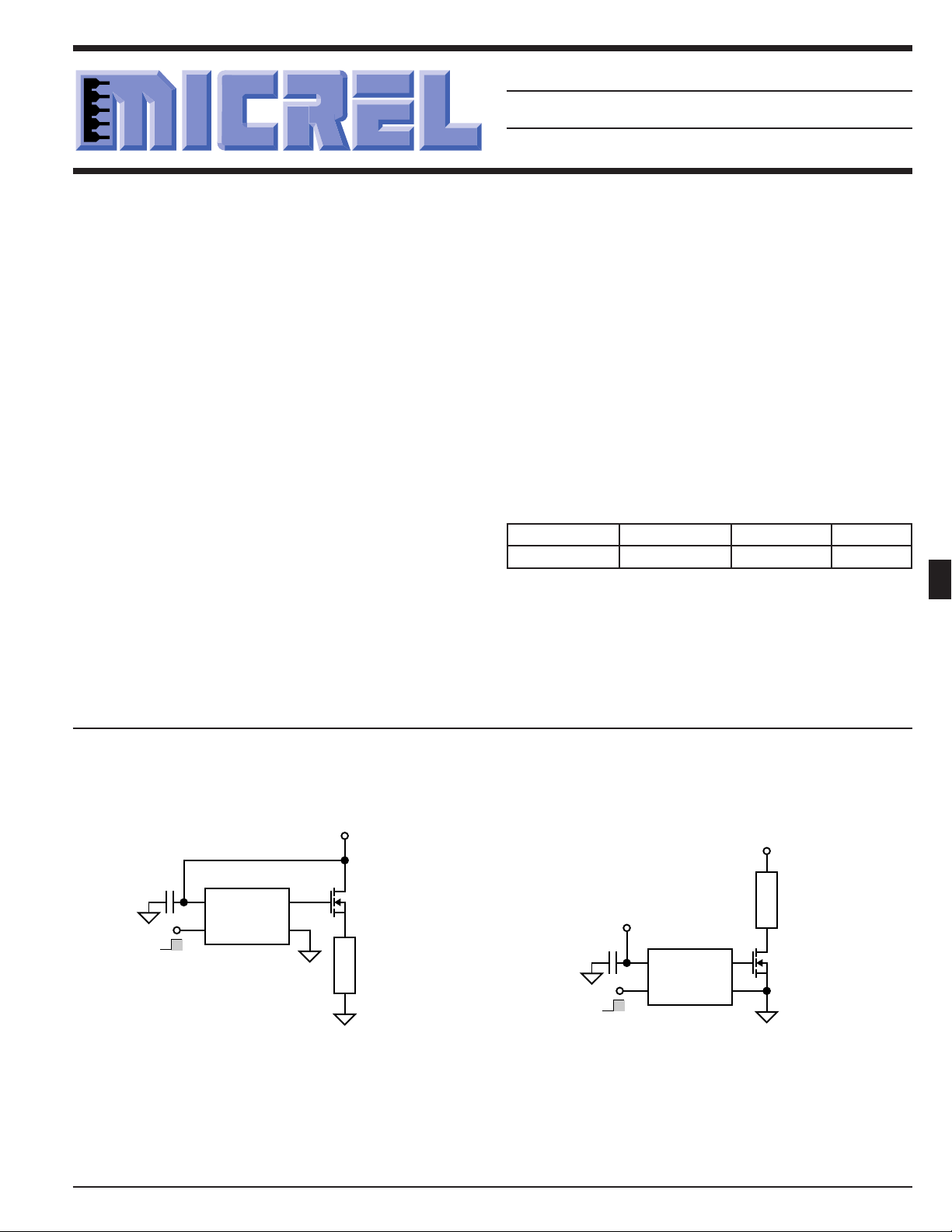
Typical Applications
+5V
4.7µF
On
Off
MIC5018
23
VS
4
CTLGGND
* International Rectifier
100m
Ω
, 17A max.
TO-220 package
1
Low-Voltage High-Side Power Switch
1997 5-155
IRFZ24*
N-Channel
MOSFET
Load
‡
Load voltage limited only by
MOSFET drain-to-source rating
* Siliconix
30m
Ω
, 7A max., 30V VDS max.
8-lead SOIC package
+2.7 to +9V
4.7µF
On
Off
23
VS
4
CTLGGND
Low-Side Power Switch
MIC5018
V
LOAD SUPPLY
1
‡
Load
Si9410DY*
N-channel
MOSFET
MIC5018 Micrel
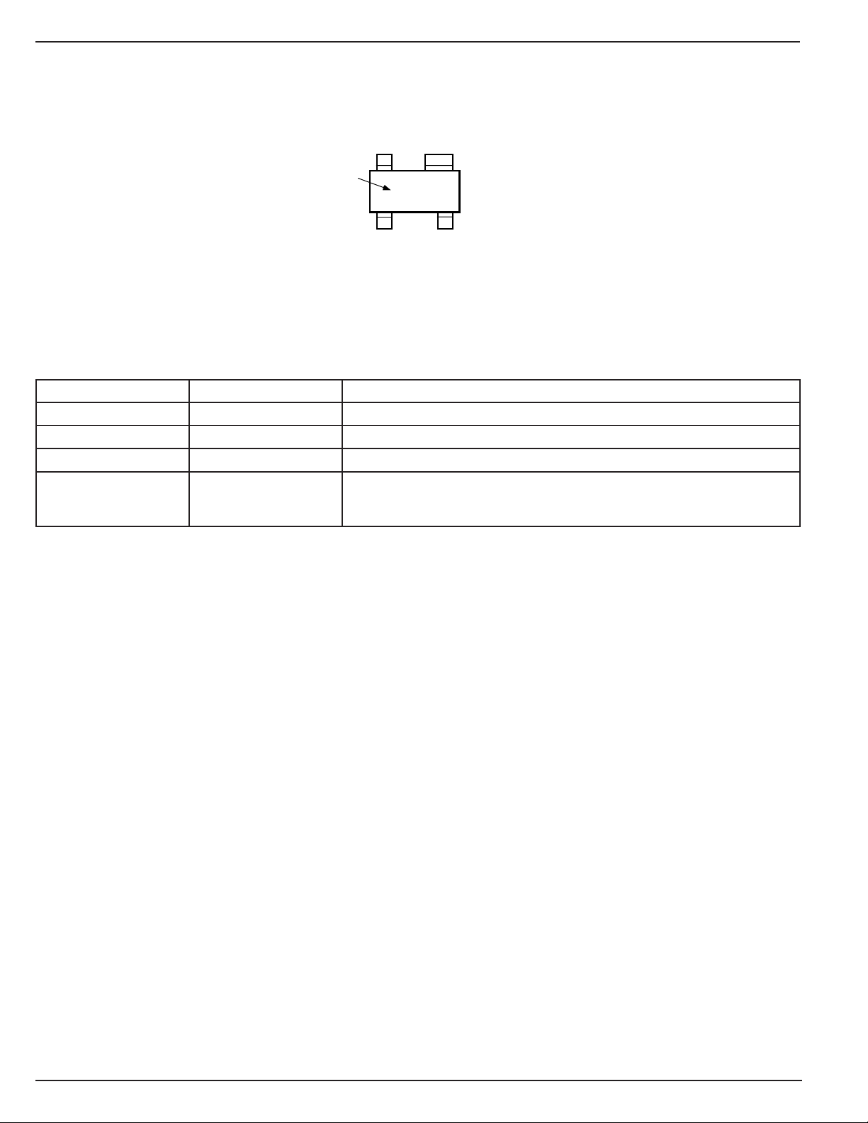
Pin Configuration
Identification
Part
Early production identification:
MH10
Pin Description
Pin Number Pin Name Pin Function
1 GND Ground: Power return.
2 VS Supply (Input): +2.7V to +9V supply.
3 G Gate (Output): Gate connection to external MOSFET.
4 CTL Control (Input): TTL compatible on/off control input. Logic high drives the
VS
GND
12
H10
34
CTLG
SOT-143 (M4)
gate output above the supply voltage. Logic low forces the gate output near
ground.
5-156 1997
MIC5018 Micrel
Absolute Maximum Ratings
Supply Voltage (V
SUPPLY
Control Voltage (V
Gate Voltage (VG) .......................................................+16V
Ambient Temperature Range (TA) ............. –40°C to +85°C
)...........................................+10V
) ................................. –0.6V to +16V
CTL
Lead Temperature, Soldering 10sec......................... 300°C
Package Thermal Resistance
SOT-143 θJA.....................................................220°C/W
SOT-143 θJC.....................................................130°C/W
Electrical Characteristics
Parameter Condition (Note 1) Min Typ Max Units
Supply Current V
V
Control Input Voltage 2.7V ≤ V
2.7V ≤ V
5V ≤ V
Control Input Current 2.7V ≤ V
Control Input Capacitance Note 2 5pF
Zener Diode Output Clamp V
Gate Output Voltage V
V
V
Gate Output Current V
Gate Turn-On Time V
Gate Turn-Off Time V
= 3.3V V
SUPPLY
= 5V V
SUPPLY
≤ 9V V
SUPPLY
≤ 5V V
SUPPLY
≤ 9V V
SUPPLY
≤ 9V 0.01 1 µA
SUPPLY
= 9V 13 16 19 V
SUPPLY
= 2.7V 6.3 7.1 V
SUPPLY
= 3.0V 7.1 8.2 V
SUPPLY
= 4.5V 11.4 13.4 V
SUPPLY
= 5V V
SUPPLY
= 4.5V CL = 1000pF, Note 4 0.75 1.5 ms
SUPPLY
= 0V 0.01 1 µA
CTL
V
= 3.3V 70 140 µA
CTL
= 0V 0 1 µA
CTL
V
= 5V 150 300 µA
CTL
for logic 0 input 0 0.8 V
CTL
for logic 1 input 2.0 V
CTL
for logic 1 input 2.4 V
CTL
= 10V, Note 3 9.5 µA
OUT
CL = 3000pF, Note 4 2.1 4.2 ms
= 4.5V CL = 1000pF, Note 5 10 20 µs
SUPPLY
CL = 3000pF, Note 5 30 60 µs
SUPPLY
SUPPLY
V
V
5
General Note: Devices are ESD protected, however handling precautions are recommended.
Note 1: Typical values at TA = 25°C. Minimum and maximum values indicate performance at –40°C ≥ TA ≥ +85°C. Parts production tested at 25°C.
Note 2: Guaranteed by design.
Note 3: Resistive load selected for V
Note 4: Turn-on time is the time required for gate voltage to rise to 4V greater than the supply voltage. This represents a typical MOSFET gate
threshold voltage.
Note 5: Turn-off time is the time required for the gate voltage to fall to 4V above the supply voltage. This represents a typical MOSFET gate threshold
voltage.
OUT
= 10V.
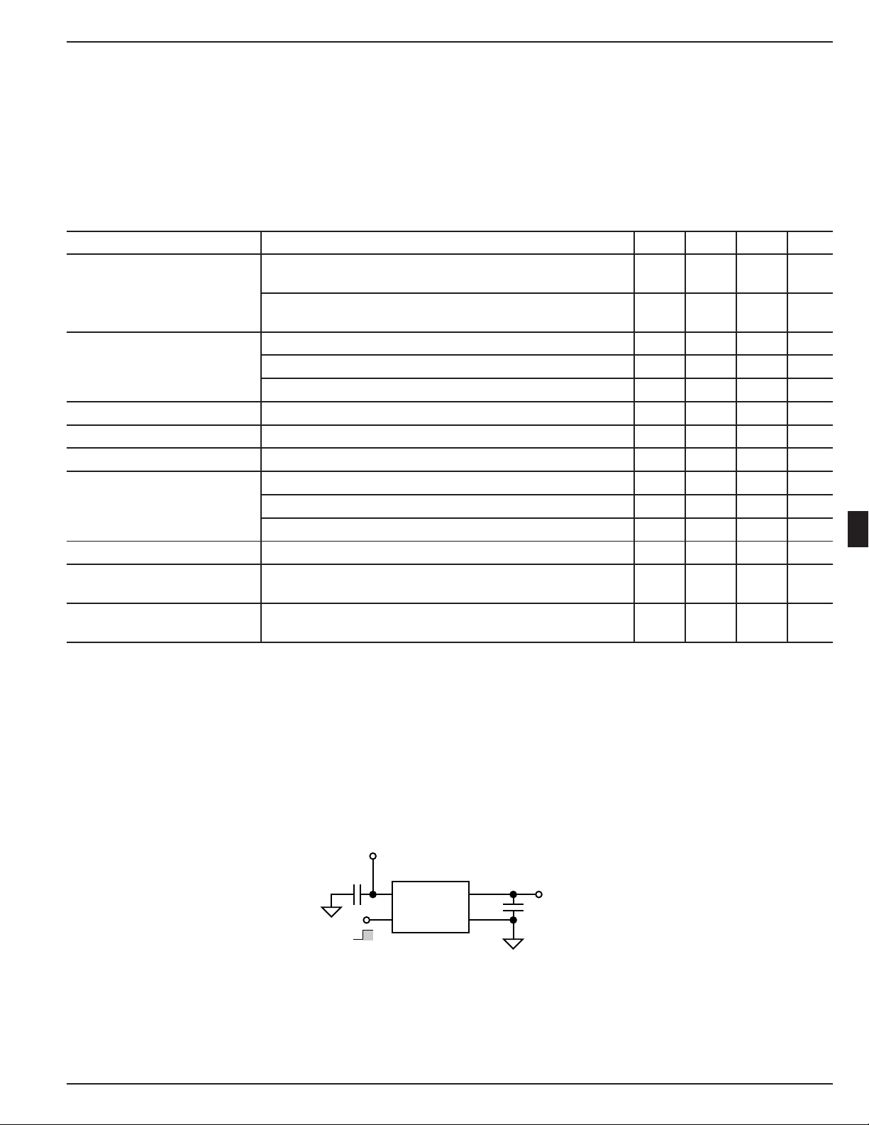
Test Circuit
V
SUPPLY
0.1µF
5V
0V
MIC5018
23
VS
4
CTLGGND
1
V
C
L
OUT
1997 5-157
 Loading...