

Micrel MIC5012 DATA SHEET
MIC5012 Micrel
MIC5012
Dual High- or Low-Side MOSFET Driver
Not Recommended for New Designs
General Description
The MIC5012 is the dual member of the Micrel MIC501X
driver family. These ICs are designed to drive the gate of an
N-channel power MOSFET above the supply rail in highside power switch applications. The 14-pin MIC5012 is
extremely easy to use, requiring only a power FET and
nominal supply decoupling to implement either a high- or
low-side switch.
The MIC5012 charges a 1nF load in 60µs typical. Operation
down to 4.75V allows the MIC5012 to drive standard
MOSFETs in 5V low-side applications by boosting the gate
voltage above the logic supply. In addition, multiple, paralleled MOSFETs can be driven by a single MIC5012 for ultrahigh current applications.
Features
• 4.75V to 32V operation
• 2 independent drivers; implements high and low side
drivers
• Less than 1µA standby current in the “off” state per
channel
• Available in small outline SOIC packages
• Internal charge pump to drive the gate of an N-channel
power FET above supply
• Internal zener clamp for gate protection
• Minimum external parts count
• Can be used to boost drive to low-side power FETs
operating on logic supplies
• Independent supply pins for half-bridge applications
Other members of the Micrel driver family include the
MIC5010 full-featured driver, MIC5011 minimum parts count
driver, and MIC5013 protected 8-pin driver.
Applications
• Lamp drivers
• Motion Control
• Heater switching
For new designs, Micrel recommends the pin-compatible
MIC5016 dual MOSFET driver.
• Power bus switching
• Half or full H-bridge drivers
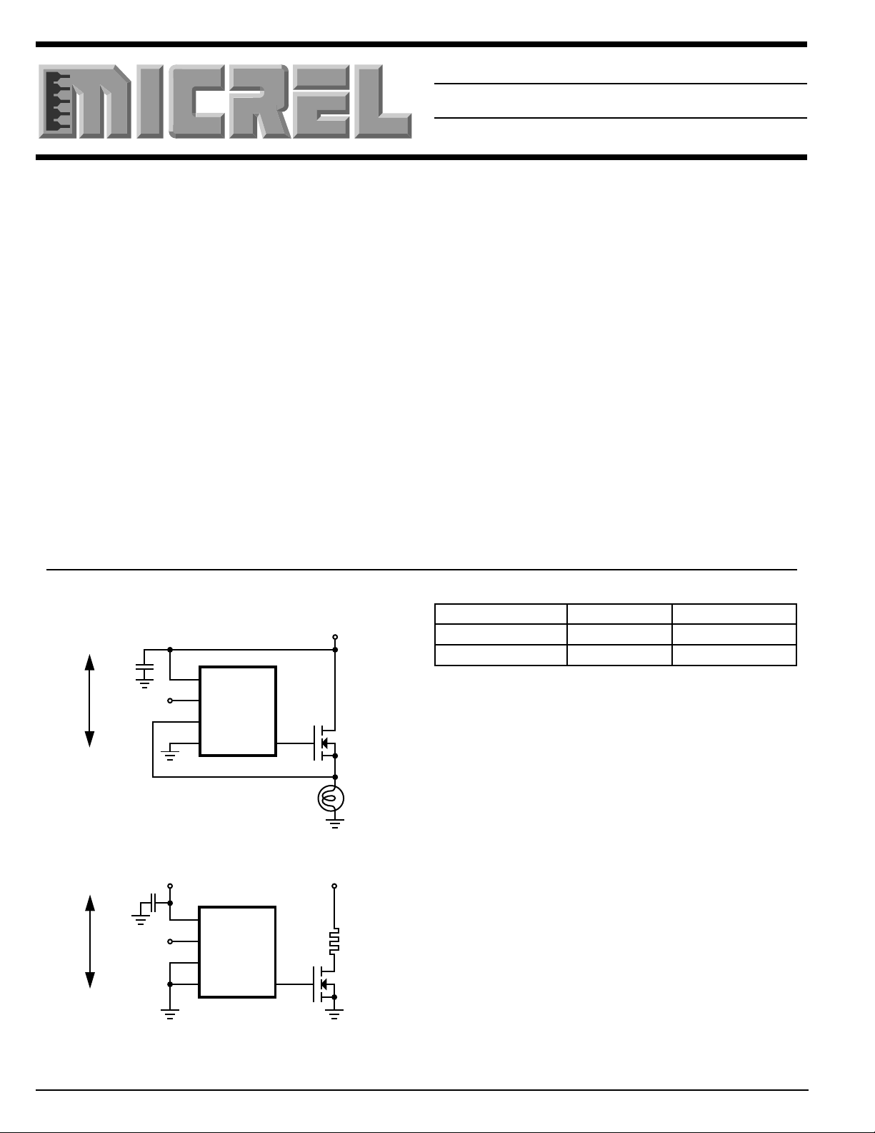
Typical Applications Ordering Information
ON
10µF
Control Input
OFF
ON
Control Input
OFF
+
1/2 MIC5012
V+
Input
Source
Gnd
Gate
Figure 1. High Side Driver
10µF
+
1/2 MIC5012
V+
Input
Source
Gnd
Gate
14.4V
48V5V
IRF531
#6014
100W
Heater
IRF530
Part Number Temp. Range Package
MIC5012BN –40°C to +85°C 14-pin Plastic DIP
MIC5012BWM –40°C to +85°C 16-pin Wide SOIC
Note: The MIC5012 is ESD sensitive.
Figure 2. Low Side Driver
Protected under one or more of the following Micrel patents:
patent #4,951,101; patent #4,914,546
5-114 April 1998
MIC5012 Micrel
34567
A
34567
A
8
Absolute Maximum Ratings (Note 1, 2)
Supply Voltage (V+), Pins 10, 12 –0.5V to 36V
Input Voltage, Pins 11, 14 –10V to V
Source Voltage, Pins 2, 5 –10V to V
Current into Pins 2, 5 50mA
Gate Voltage, Pins 4, 6 –1V to 50V
Junction Temperature 150°C
Pin Description (Refer to Typical Applications)
DIP Pin Number Pin Name Pin Function
12, 10 V
14, 11 Input Turns on power MOSFET when taken above threshold (3.5V typical).
2, 5 Source Connects to source lead of power FET and is the return for the gate clamp
3 Ground
4, 6 Gate Drives and clamps the gate of the power FET. Clamped to approximately –
+
Supply; must be decoupled to isolate from large transients caused by the
power FET drain. 10µF is recommended close to pins 1 and 4.
Requires <1 µA to switch.
zener. Can safely swing to –10V when turning off inductive loads.
0.7V by an internal diode when turning off inductive loads.
Operating Ratings (Notes 1, 2)
Power Dissipation 1.56W
+
θJA (Plastic DIP) 80 °C/W
+
θJA (SOIC) 105°C/W
Ambient Temperature: B version –40°C to +85°C
Storage Temperature –65°C to +150°C
Lead Temperature 260°C
(Soldering, 10 seconds)
Supply Voltage (V+), Pin 1 4.75V to 32V high side
4.75V to 15V low side
5
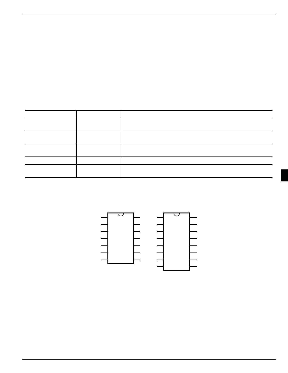
Pin Configuration
MIC5012 (N, J)
1
2
Input A
NC
Source A
Gnd
Source B V+ B
Gate B
NC
V+
Input BGate A
NC
NC
NC
14
13
12
11
10
MIC5012 (WM)
1
NC
2
Source A
Gnd
Source B V+ B
9
8
Gate B
NC
NC
Input A
NC
V+
Input BGate A
NC
NC
NC
16
15
14
13
12
11
10
9
April 1998 5-115
MIC5012 Micrel
Electrical Characteristics (Note 3) Test circuit. T
= –55°C to +125°C, V+ = 15V, all switches open, unless
A
otherwise specified.
Parameter Conditions Min Typical Max Units
Supply Current V+ = 32V VIN = 0V, S2 closed 0.1 10 µA
(per section) VIN = VS = 32V 8 20 mA
V+ = 5V VIN = 5V, S2 closed 1.6 4 mA
Logic Input Voltage V+ = 4.75V Adjust VIN for V
Adjust VIN for V
V+ = 15V Adjust VIN for V
Logic Input Current, I
2
V+ = 32V VIN = 0V –1 µA
VIN = 32V 1 µA
Input Capacitance Pins 11, 14 5 pF
Gate Drive, V
GATE
S1, S2 closed, V+ = 4.75V, I
VS = V+, VIN = 5V V+ = 15V, I
GATE
GATE
Zener Clamp, S2 closed, VIN = 5V V+ = 15V, VS = 15V 11 12.5 15 V
V
– V
GATE
Gate Turn-on Time, t
(Note 4) for V
Gate Turn-off Time, t
Note 1 Absolute Maximum Ratings indicate limits beyond which damage to the device may occur. Electrical specifications do not apply when
Note 2 The MIC5012 is ESD sensitive.
Note 3 Minimum and maximum Electrical Characteristics are 100% tested at TA = 25°C and TA = 85°C, and 100% guaranteed over the entire
Note 4 Test conditions reflect worst case high-side driver performance. Low-side and bootstrapped topologies are significantly faster—see
SOURCE
ON
OFF
operating the device beyond its specified Operating Ratings.
range. Typicals are characterized at 25°C and represent the most likely parametric norm.
Applications Information. Maximum value of switching speed seen at 125°C, units operated at room temperature will reflect the typical
values shown.
VIN switched from 0 to 5V; measure time 60 200 µs
to reach 20V
GATE
VIN switched from 5 to 0V; measure time 4 10 µs
for V
to reach 1V
GATE
V+ = 32V, VS = 32V 11 13 16 V
low 2 V
GATE
high 4.5 V
GATE
high 5.0 V
GATE
= 0, VIN = 4.5V 7 10 V
= 100µA, VIN = 5V 24 27 V
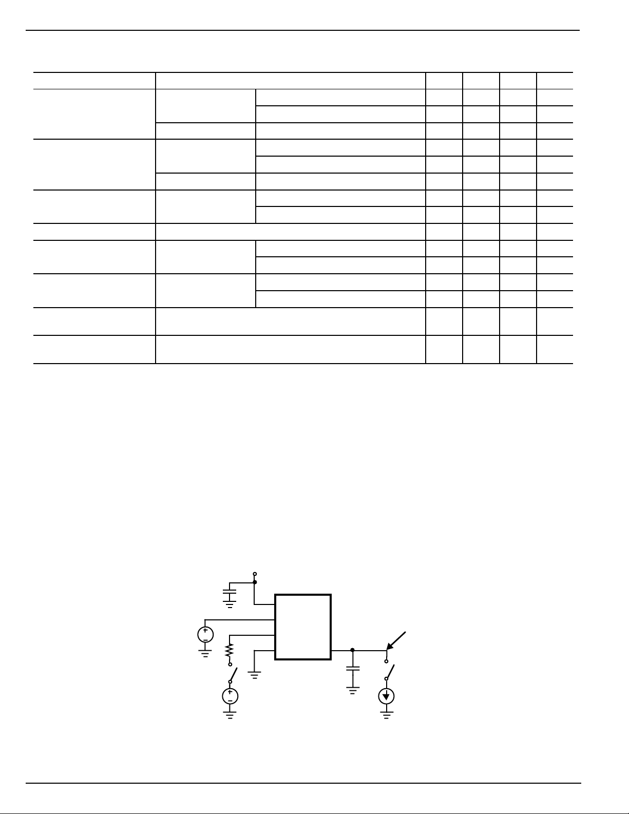
Test Circuit
V+
+
1µF
V
IN
500Ω
1W
S2
VS
1/2 MIC5012
V+
Input
Source
Gnd
Gate
1nF
S1
I
V
GATE
GATE
5-116 April 1998
 Loading...