

Page 1
General Description
MIC45208 Evaluation Board
26V/10A DC-to-DC Power Module
Getting Started
Micrel’s MIC45208 is a synchronous step-down regulator
module, featuring a unique adaptive ON-time control
architecture. The module incorporates a DC-to-DC
controller, power MOSFETs, bootstrap diode, bootstrap
capacitor, and an inductor in a single package; sim plifying
the design and layout process for the end user.
This highly-integrated solution expedites system design
and improves product time-to-market. The internal
MOSFETs and inductor are optimized to achieve high
efficiency at a low output voltage. The fully optimized
design can deliver up to 10A current under a wide input
voltage range of 4.5 V to 26V, without requiring add itional
cooling.
®
The MIC45208-1 uses Micrel’s HyperLight Load
(HLL)
MIC45208-2 uses Micrel’s Hyper Speed Control™
architecture which enables ultra-fast load transient
response, allowing for a reduction of output capacitance.
The MIC45208 offers 1% output accuracy that can be
adjusted from 0.8V to 5.5V with two external resistors.
The basic parameters of the evaluation board are:
• Input: 4.5V to 26V
• Output: 0.8V to 5V at 10A
• 600kHz Switching Frequency
(Adjustable 200kHz to 600kHz)
Datasheets and support documentation are available on
Micrel’s web site at: www.micrel.com
.
Requirements
The MIC45208-1 and MIC45208-2 evaluation board only
requires a single power supply with at least 10A current
capability. No external linear r egulator is requ ired to p ower
the internal biasing of t he IC because the MIC45208 has
an internal PVDD LDO. In applications where VIN < +5.5V,
PVDD shoul d be tied to VIN to bypass the internal linear
regulator. The output load can either be a passive or an
active load.
1. VIN Supply
Connect a power supply to the VIN and GND
terminals, paying careful attention to the polarity and
the supply range (4.5V < V IN < 26V). Monitor IIN with
a current meter and monitor input vol tage at VIN and
GND terminals with a voltmeter. Do not apply power
until Step 4.
2. Connect Load and Monitor Output
Connect a load to the VOUT and GND terminals. The
load can be either a pas si v e (r es isti ve) or a n ac t ive ( a s
in an electronic load) type. A current meter may be
placed between the VOUT terminal and load to
monitor the output current. Ensure the output voltage
is monitored at the VOUT terminal.
3. Enable Input
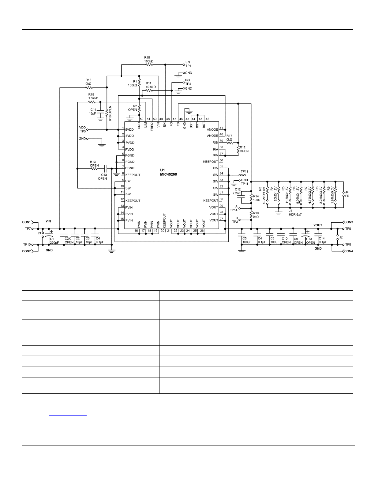
The EN pin has an on-board 100kΩ pull-up resistor
(R10) to VIN, which allo ws the output to be turned o n
when PVDD exceeds its UVLO threshold. An EN
connector is provided on the evaluation board for
users to easily acc ess the enable feature. Ap plying an
external logic signal on the EN pin to pull it low or
using a jumper to short the EN pin to G ND will shut off
the output of the MIC45208 evaluation board .
4. Turn Power On
Turn on the VIN supply and verify that the output
voltage is regulated to 5V.
Ordering Information
Part Number Description
MIC45208-1YMP EV MIC45208-1 Evaluation Board
MIC45208-2YMP EV MIC45208-2 Evaluation Board
Precautions
The MIC45208 evaluation board does not have reverse
polarity protection. Applying a negative voltage to the VIN
and GND terminals can damage the de vice . The maximum
VIN of the board is rated at 30V. Exceeding 30V on the
VIN could damage the device.
HyperLight Load is a registered trademark and Hyper Speed Control is a trademark of Micrel, Inc.
Micrel Inc. • 2180 Fortune Drive • San Jose, CA 95131 • USA • tel +1 (408) 944-0800 • fax + 1 (408) 474-1000 • http://www.micrel.com
August 19, 2015
Revision 2.0
Page 2
Micrel, Inc.
MIC45208 Evaluation Board
A
+×=
BOTTOM
REF
OUT
R
R14
1VV
REFOUT
REF
BOTTOM
VV
VR1
R
−
×
=
(Top Feedback Resistor)
(Bottom Feedback Resistor)
Features
Feedback Resistors
The output voltage on the MIC45208 evaluation board,
which is preset to 5.0V, is determined by the feedback
All other voltages not listed abo ve can b e set b y modifying
R
value according to:
BOTTOM
divider:
where V
REF
Leaving the R
= 0.8V, and R
open by removing all jum pers on the
BOTTOM
Eq. 1
is one of R3 thru R9.
BOTTOM
Eq. 2
Note that the output volt age should not be set to exceed
5V.
feedback headers gives a 0.8V output voltage.
Table 1. Typical Values of Some Components
V
VIN
OUT
1.0V 5V to 26V 10kΩ 40.2kΩ 2.2nF 100µF/6.3V
1.2V 5V to 26V 10kΩ 20kΩ 2.2nF 100µF/6.3V
R14
R
C12
(C
ff
C
)
OUT
1.5V 5V to 26V 10kΩ 11.5kΩ 2.2nF 100µF/6.3V
1.8V 5V to 26V 10kΩ 8.06kΩ 2.2nF 100µF/6.3V
2.5V 5V to 26V 10kΩ 4.75kΩ 2.2nF 100µF/6.3V
3.3V 5V to 26V 10kΩ 3.24kΩ 2.2nF 100µF/6.3V
5V 7V to 26V 10kΩ 1.9kΩ 2.2nF 100µF/6.3V
ugust 19, 2015 2
Revision 2.0
Page 3
Micrel, Inc.
MIC45208 Evaluation Board
A
( )
CL
CL)ON(DS
PP
LCLIM
I
VR)5.0II(
R15
+××D−
=
L f V
)V(VV
I
swIN(MAX)
OUTIN(MAX)OUT
L(PP)
××
−×
=D
SW Node
Test point TP12 (V
) is placed for monitoring the
SW
switching waveform, which is one of the most critical
waveforms for the converter.
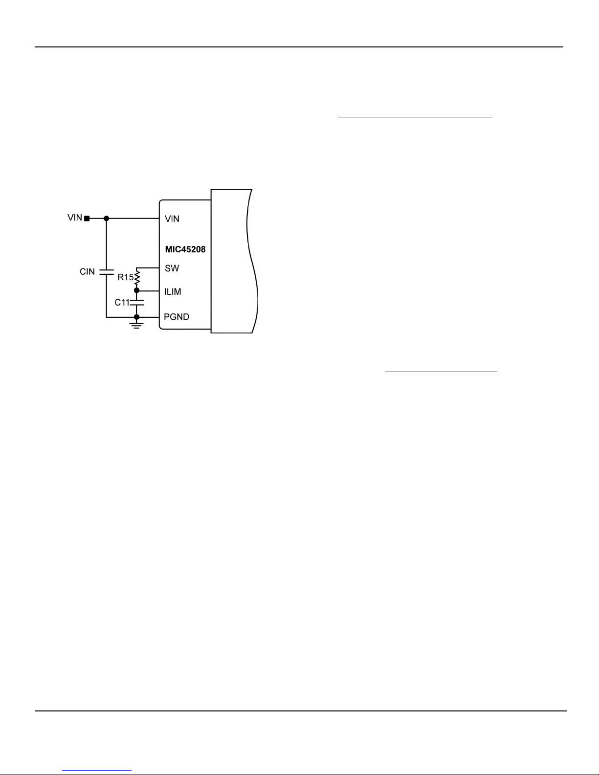
The short circuit curr ent lim it can be pro gramm ed by using
the following formula:
Current Limit
The MIC45208 uses the R
of the l ow-side MOSFET
DS(ON)
and external resistor connected from the ILIM pin to the
SW node to decide the current limit.
Figure 1. MIC45208 Current Limiting Circuit
During each switching c ycle of the MIC 45208, th e induc tor
current is sensed by monitoring the low-side MOSFET in
the OFF period. The sensed voltage, V
, is compared
(ILIM)
with the power ground (PGND) after a blanking time of
150ns. In this way the drop voltage over the resistor R15
) is compared with the drop over the bottom FET
(V
CL
generating the short current limit. The small capacitor
(C11) connected from ILIM pin to PGND filters the
switching node ringi ng duri ng the off-t ime allowing a better
short-limit measurement. The time constant created by
R15 and C11 should be muc h less than the minimum off
time.
The V
drop allows progr a m m ing of s hor t lim it thr oug h the
CL
value of the resistor (R15) if the absolute value of the
voltage drop on the bott om F ET is greater th an V
case the V
is lower than PGND and a short circuit
(ILIM)
. In that
CL
event is triggered. A hiccup c ycle to treat the s hort eve nt is
generated. The hiccup sequence including the soft start
reduces the stress on the switc hing FETs and protec ts the
load and supply for severe short conditions.
Eq. 3
I
= Desired current limit
CLIM
R
= On-resistance of low-side power MO SFET, 6mΩ
DS(ON)
(typ.)
= Current-limit threshold (typical absolute value is
V
CL
14mV per Electrical Characteristics table in MIC45208
datasheet)
= Current-limit source current (typical value is 70µA,
I
CL
per the Electrical Characteristics table in MIC45208
datasheet).
= I nductor current peak-to-peak, since the inductor
ΔI
L(PP)
is integrated use Equation 4 to calcu lat e t he in duc tor ripple
current.
The peak-to-peak inductor current ripple is:
Eq. 4
The MIC45208 has 0.8µH inductor integrated into the
module. In case of hard short, the short limit is folded
down to allow an indefinite hard short on the output without
any destructive effect. It is mandatory to make sure that
the inductor current use d to charge th e output c apacitance
during soft-start is under the folded short limit; otherwise
the supply will go in hiccup mode and m ay not be f inishing
the soft start successfully.
The MOSFET R
Therefore, it is recomm ended to add a 50% margin to I
DS(ON) varies 30 to 40% with temperature.
CLIM
in the above equation to avoid f alse current limiting du e to
increased MOSFET junction temperature r ise. With R15 =
1.37kΩ and C11 = 15pF, the t ypical output current lim it is
16.8A.
ugust 19, 2015 3
Revision 2.0
Page 4
Micrel, Inc.
MIC45208 Evaluation Board
A
2R1R
2R
ff
OSW
+
×=
0
100
200
300
400
500
600
700
800
10.00 100.00 1000.00 10000.00
SW FREQ (kHz)
R2 (kΩ)
Switching Frequency
V
OUT
= 5V
V
= 12V
R1 = 100kΩ
Setting the Switching Frequency
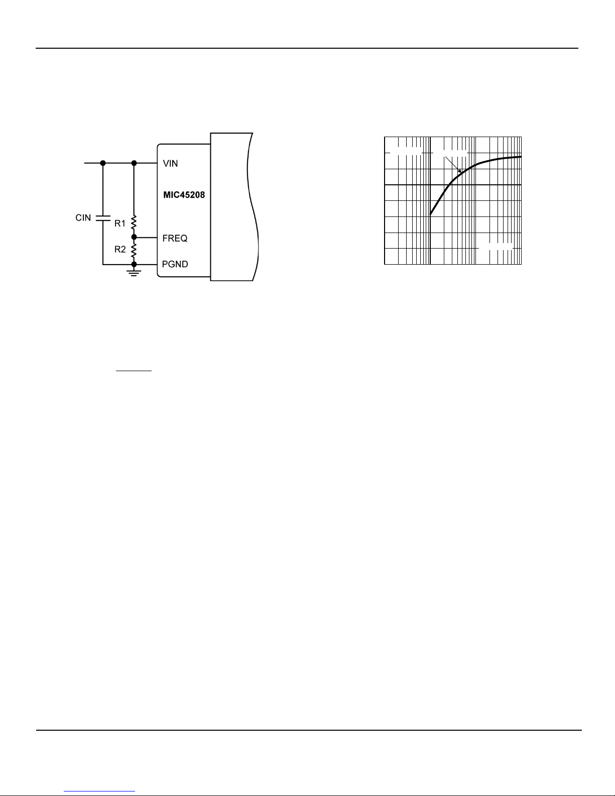
The MIC45208 switching frequency can be adjusted by
changing the value of res istors R1 and R2. The switching
, V
frequency also depends on V
IN
, and load conditions.
OUT
R2 is selected to s et the required switching frequenc y as
shown in Figure 3:
Figure 2. Switching Frequency Adjustment
Equation 5 illustrates the estimated switching frequency:
Eq. 5
Where fO = 600kHz
R1 = 100kΩ (recommended)
Figure 3. Switching Frequency vs. R2
ugust 19, 2015 4
Revision 2.0
Page 5
Micrel, Inc.
MIC45208 Evaluation Board
A
C11
MIC45208 Evaluation Board Schematic
Bill of Materials
Item Part Number Manufacturer Description Qty.
C1 B41125A7227M000 TDK(1) 220µF/35V, ALE Capacitor (optional) 1
C2, C3 C3216X5R1H106M160AB TDK 10µF/50V, 1206, X5R, 10%, MLCC 2
C2X, C9, C10, C7,
C7X, C13
C4, C8, C14 GRM188R71H104KA93D Murata(2) 0.1µF/50V, X7R, 0603, 10%, MLCC 3
C5, C6 C3216X5R0J107M160AB TDK 100µF/6.3V, X5R, 1206, 20%, MLCC 2
C11 GRM1885C1H150JA01D Murata 15pF/50V, NP0, 0603, 5%, MLCC 3
C12 C1608C0G1H222JT TDK 2.2nF/50V, NP0, 0603, 5%, MLCC 1
CON1, CON2,
CON3, CON4
Notes:
1. TDK: www.TDK.com
2. Murata: www.murata.com.
3. Keystone: www.keyelco.com.
Open 6
(3)
8191k Keystone
.
15A, 4-Prong Through-Hole Screw Terminal 4
ugust 19, 2015 5
Revision 2.0
Page 6
Micrel, Inc.
MIC45208 Evaluation Board
A
Item
Part Number
Manufacturer
Description
Qty.
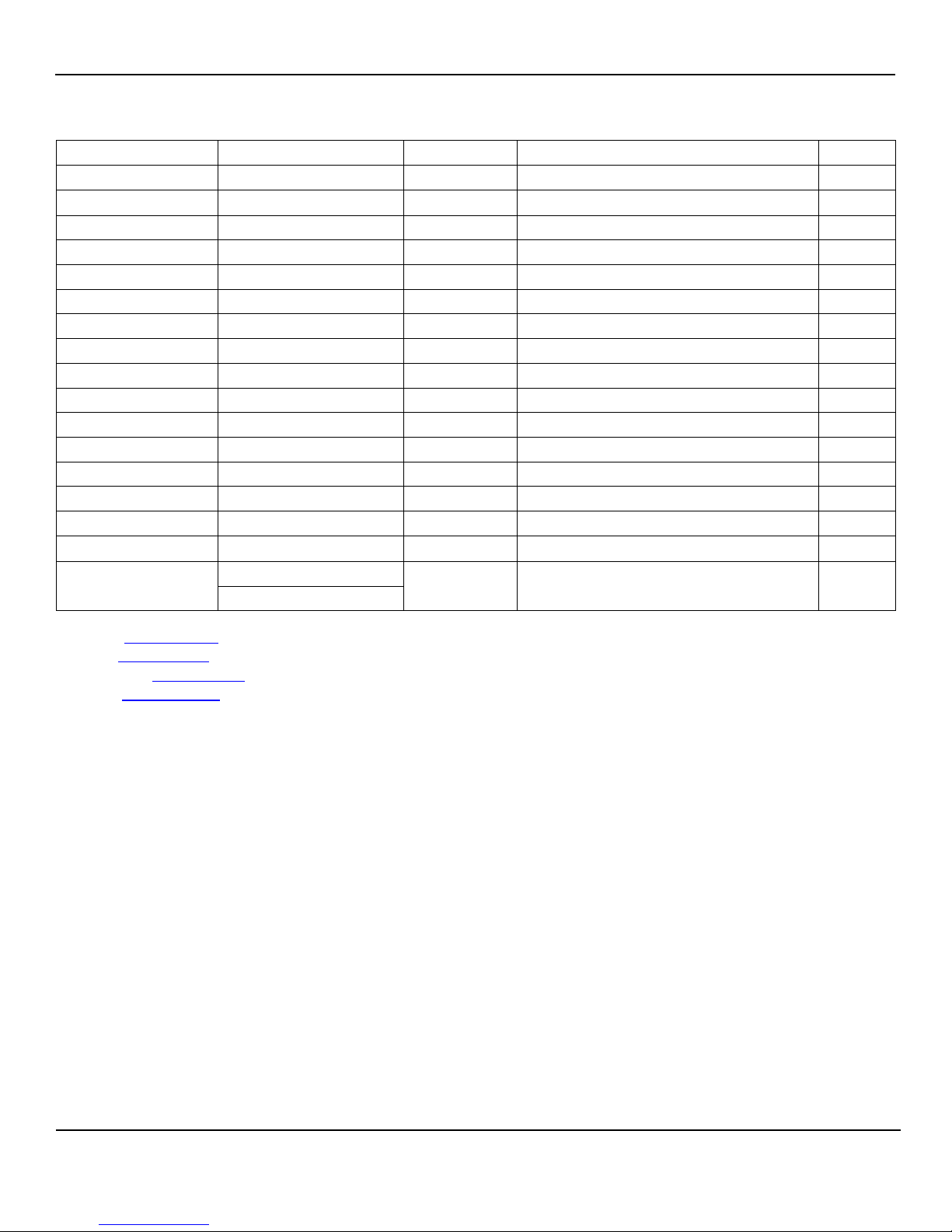
Bill of Materials (Continued)
J1 M50-3500742 Harwin(4) Header 2x7 1
J2, J3, J4, TP3 − TP5
R1, R10 CRCW0603100K0FKEA Vishay Dale(6) 100kΩ, 1%, 1/10W, 0603, Thick Film 2
R2, R12, R13, R16 Open 4
R3 CRCW060340K2FKEA Vishay Dale 40.2kΩ, 1%, 1/10W, 0603, Thick Film 1
R4 CRCW06020K0FKEA Vishay Dale 20kΩ, 1%, 1/10W, 0603, Thick Film 1
R5 CRCW060311K5FKEA Vishay Dale 11.5kΩ, 1%, 1/10W, 0603, Thick Film 1
R6 CRCW06038K06FKEA Vishay Dale 8.06kΩ, 1%, 1/10W, 0603, Thick Film 1
R7 CRCW06034K75FKEA Vishay Dale 4.75kΩ, 1%, 1/10W, 0603, Thick Film 1
R8 CRCW06033K24FKEA Vishay Dale 3.24kΩ, 1%, 1/10W, 0603, Thick Film 1
R9 CRCW06031K91FKEA Vishay Dale 1.91kΩ, 1%, 1/10W, 0603, Thick Film 1
R11 CRCW060349K9FKEA Vishay Dale 49.9kΩ, 1%, 1/10W, 0603, Thick Film 1
R14 CRCW060310K0FKEA Vishay Dale 10kΩ, 1%, 1/10W, 0603, Thick Film 1
R15 CRCW06031K37FKEA Vishay Dale 1.37kΩ, 1%, 1/10W, 0603, Thick Film 1
R17, R18, R19 RCG06030000Z0EA Vishay Dale 0Ω Resistor, 1%, 1/10W, 0603, Thick Film 3
TP7 − TP14
U1
Notes:
4. Harwin: www.harwin.com
5. Molex: www.molex.com.
6. Vishay-Dale: www.vishay.com.
7. Micrel: www.micrel.com.
90120-0122 Molex(5) Header 2 6
1502-2 Keystone Single-End, Through-Hole Terminal 8
MIC45208-1YMP
MIC45208-2YMP
.
Micrel, Inc.(7) 26V/10A DC-to-DC Power Module 1
ugust 19, 2015 6
Revision 2.0
Page 7
Micrel, Inc.
MIC45208 Evaluation Board
A
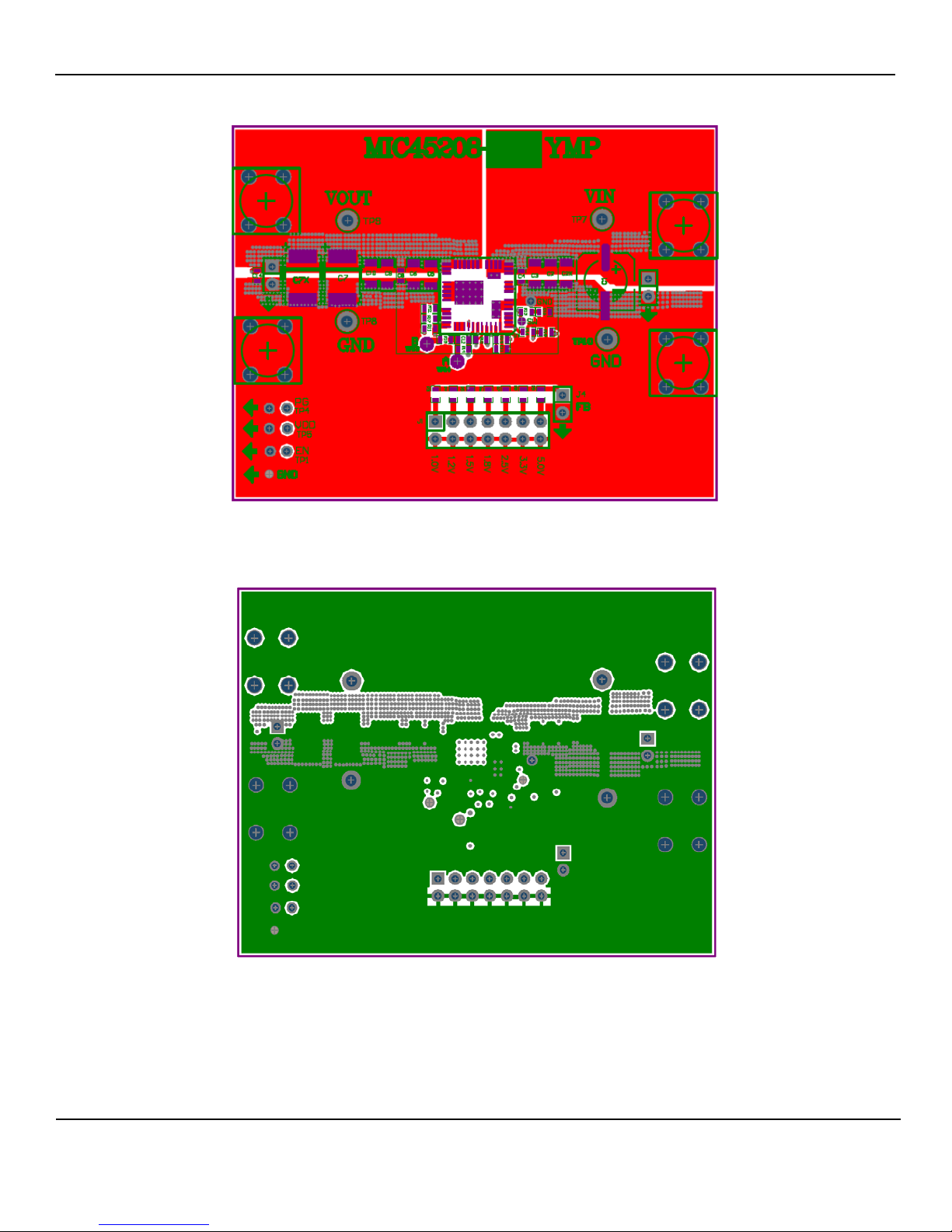
PCB Layout Recommendations
MIC45208 Evaluation Board Top Layer
ugust 19, 2015 7
MIC45208 Evaluation Board Copper Layer 2
Revision 2.0
Page 8
Micrel, Inc.
MIC45208 Evaluation Board
A
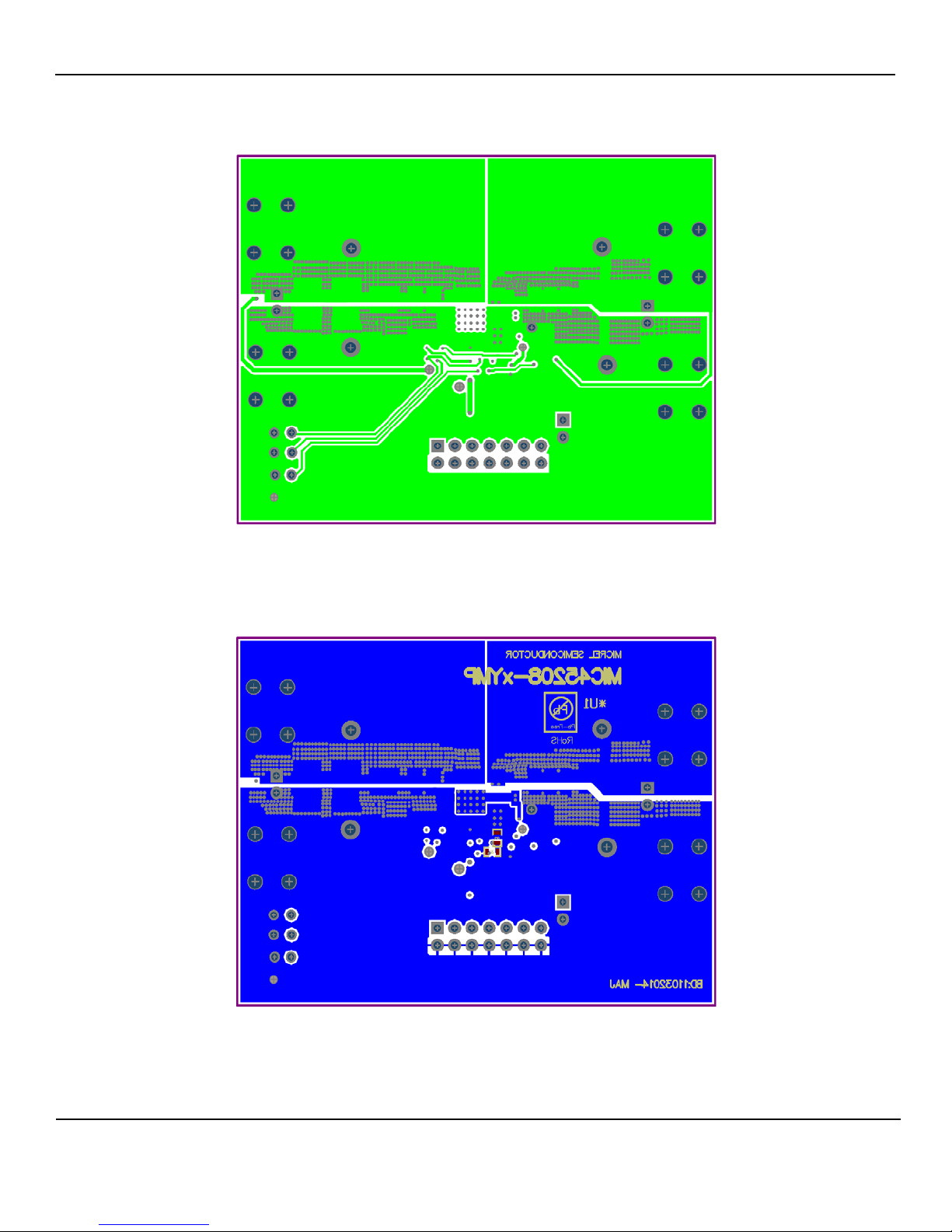
PCB Layout Recommendations (Continued)
MIC45208 Evaluation Board Copper Layer 3
ugust 19, 2015 8
MIC45208 Evaluation Board Bottom Layer
Revision 2.0
Page 9

Micrel, Inc.
MIC45208 Evaluation Board
A
MICREL, INC. 2180 FORTUNE DRIVE SAN JOSE, CA 95131 USA
Micrel, Inc. is a leading global m anufacturer of IC sol utions for the worldwide high
communications
markets. The Company’s products include advanced mixed
performance communication, clock
management,
Company
customers include leading manufacturers of enterprise, consumer, industrial, mobile, telecommunications, automotive, and comp
Corporation headquarters and state
ed in San Jose, CA, with regional sales and support offices and
advanced technology design centers situated throughout t he Americas, Europe, and Asia. Additionally, the Company maintains an extensive network
of distributors and reps worldwide.
Micrel mak
sheet. This
information is not intended as a warranty and Micrel does not assume responsibility for its use.
t to change circuitry,
specifications and descriptions at any ti me without notice. No license, whether express, implied, arising by estoppel or otherwise, to any intell ectual
property rights
s and conditions of sale for suc h products, Micrel assumes no li ability
whatsoever, and Micrel disclaims any express or implied warranty relati ng to the sale and/or use of Micrel products including liability or warranties
relating to fitness for a particul
Micrel Products are not designed or authorized for use as com ponents in life support appliances, devices or systems where malf unction of a product
can reasonably be expected to result in personal injury. Life support devices or syst ems are devices or systems that (a) are intended for surgical
implant into the body or (b) support or sustain life, and whose fai l ure to perform can be reasonably expected to result in a signific ant injury t o t he user. A
Purchaser’s use or sale of Micrel Products for use in life support appliances, devices or systems is a Purchaser’s own risk and Purchaser agrees to fully
indemnify Micrel for any damages resulting from suc
TEL +1 (408) 944-0800 FAX +1 (408) 474-1000 WEB http://www.micrel.com
MEMs-based clock oscillators & crystal-less clock generators, Ethernet switches, and physical layer transceiver ICs.
-of-the-art wafer fabrication facilities are locat
es no representations or warranties with respect to the accuracy or completeness of the information furnished in this data
ugust 19, 2015 9
is grant ed by this document. E xcept as provided in Micrel’s term
ar purpose, merchantability, or infringement of any patent, copyright, or other intellectual property ri ght.
h use or sale.
-signal, analog & power semiconductors; high-
© 2015 Micrel, Incorporated.
-performance linear and power, LAN, and timing &
Micrel reserves the righ
uter products.
Revision 2.0
 Loading...