


MICREL MIC4425BWM, MIC4425CN, MIC4425CWM, MIC4425BM, MIC4424CWM Datasheet
...
MIC4423/4424/4425 Micrel
MIC4423/4424/4425
Dual 3A-Peak Low-Side MOSFET Driver
Bipolar/CMOS/DMOS Process
General Description
The MIC4423/4424/4425 family are highly reliable BiCMOS/
DMOS buffer/driver/MOSFET drivers. They are higher output
current versions of the MIC4426/4427/4428, which are
improved versions of the MIC426/427/428. All three families
are pin-compatible. The MIC4423/4424/4425 drivers are
capable of giving reliable service in more demanding electrical
environments than their predecessors. They will not latch
under any conditions within their power and voltage ratings.
They can survive up to 5V of noise spiking, of either polarity,
on the ground pin. They can accept, without either damage or
logic upset, up to half an amp of reverse current (either
polarity) forced back into their outputs.
The MIC4423/4424/4425 series drivers are easier to use,
more flexible in operation, and more forgiving than other
CMOS or bipolar drivers currently available. Their BiCMOS/
DMOS construction dissipates minimum power and provides
rail-to-rail voltage swings.
Primarily intended for driving power MOSFETs, the MIC4423/
4424/4425 drivers are suitable for driving other loads
(capacitive, resistive, or inductive) which require lowimpedance, high peak currents, and fast switching times.
Heavily loaded clock lines, coaxial cables, or piezoelectric
transducers are some examples. The only known limitation on
loading is that total power dissipated in the driver must be kept
within the maximum power dissipation limits of the package.
Features
• Reliable, low-power bipolar/CMOS/DMOS construction
• Latch-up protected to >500mA reverse current
• Logic input withstands swing to –5V
• High 3A-peak output current
• Wide 4.5V to 18V operating range
• Drives 1800pF capacitance in 25ns
• Short <40ns typical delay time
• Delay times consistent with in supply voltage change
• Matched rise and fall times
• TTL logic input independent of supply voltage
• Low equivalent 6pF input capacitance
• Low supply current
3.5mA with logic-1 input
350µA with logic-0 input
• Low 3.5Ω typical output impedance
• Output voltage swings within 25mV of ground or VS.
• ‘426/7/8-, ‘1426/7/8-, ‘4426/7/8-compatible pinout
• Inverting, noninverting, and differential configurations
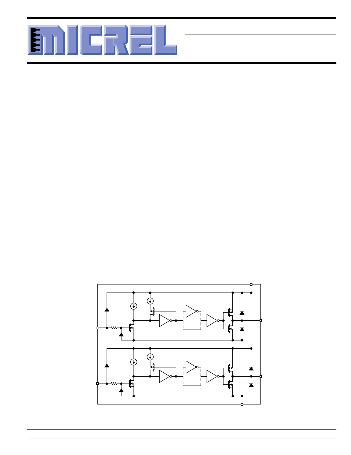
Functional Diagram
V
S
Integrated Component Count:
4 Resistors
INVERTING
NONINVERTING
INVERTING
NONINVERTING
GND
INA
INB
0.1mA
0.6mA
2kΩ
0.6mA
0.1mA
2kΩ
Ground Unused Inputs
Micrel, Inc. • 1849 Fortune Drive • San Jose, CA 95131 • USA • tel + 1 (408) 944-0800 • fax + 1 (408) 944-0970 • http://www.micrel.com
January 1999 1 MIC4423/4424/4425
4 Capacitors
52 Transistors
OUTA
OUTB
MIC4423/4424/4425 Micrel
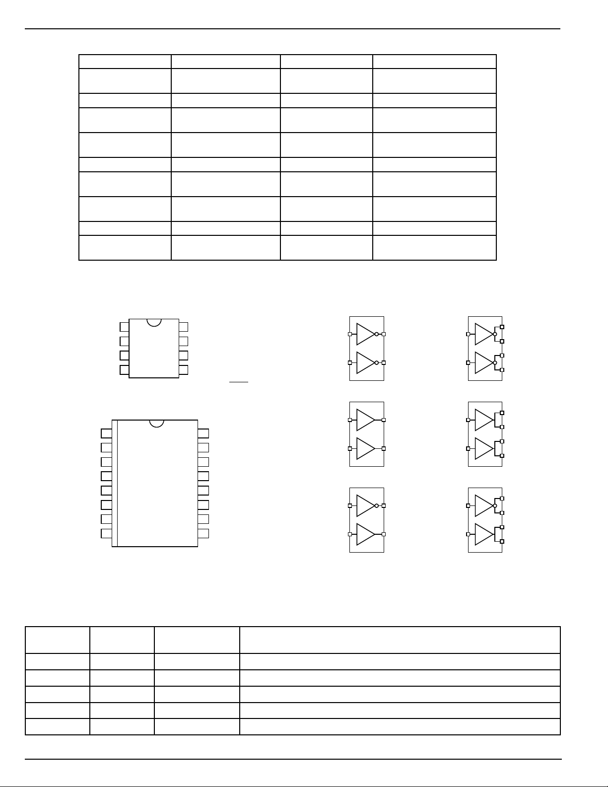
Ordering Information
Part Number Temperature Range Package Configuration
MIC4423CWM 0°C to +70°C 16-Pin Wide SOIC Dual Inverting
MIC4423BWM –40°C to +85°C
MIC4423BM –40°C to +85°C 8-Pin SOIC Dual Inverting
MIC4423CN 0°C to +70°C 8-Pin Plastic DIP Dual Inverting
MIC4423BN –40°C to +85°C
MIC4424CWM 0°C to +70°C 16-Pin Wide SOIC Dual Non-Inverting
MIC4424BWM –40°C to +85°C
MIC4424BM –40°C to +85°C 8-Pin SOIC Dual Non-Inverting
MIC4424CN 0°C to +70°C 8-Pin Plastic DIP Dual Non-Inverting
MIC4424BN –40°C to +85°C
MIC4425CWM 0°C to +70°C 16-Pin Wide SOIC Inverting + Non Inverting
MIC4425BWM –40°C to +85°C
MIC4425BM –40°C to +85°C 8-Pin SOIC Inverting + Non Inverting
MIC4425CN 0°C to +70°C 8-Pin Plastic DIP Inverting + Non Inverting
MIC4425BN –40°C to +85°C
Pin Configuration
NC
1
INA
2
GND
3
INB
4
8-pin SOIC (M)
1NC
2INA
8NC
16-lead Wide SOIC (WM)
8-pin DIP (N)
8
7
6
5
NC
OUTA
VS
OUTB
WM Package Note:
Duplicate
OUTA
, and
must be externally
connected together.
NC16
OUTA15
OUTA143NC
VS134GND
VS125GND
OUTB116NC
OUTB107INB
NC9
GND, VS
OUTB
Driver Configuration
MIC4423xN/M
A
7 OUTA
B
5 OUTB
A
7 OUTA
B
5 OUTB
A
7 OUTA
B
5 OUTB
,
pins
INA 2
INB 4
MIC4424xN/M
INA 2
INB 4
MIC4425xN/M
INA 2
INB 4
MIC4423xWM
INA 2
INB 7
MIC4424xWM
INA 2
INB 7
MIC4425xWM
INA 2
INB 7
14 OUTA
A
15 OUTA
10 OUTB
B
11 OUTB
14 OUTA
A
15 OUTA
10 OUTB
B
11 OUTB
14 OUTA
A
15 OUTA
10 OUTB
B
11 OUTB
Pin Description
Pin Number Pin Number Pin Name Pin Function
DIP, SOIC Wide SOIC
2 / 4 2 / 7 INA/B Control Input
3 4, 5 GND Ground: Duplicate pins must be externally connected together.
6 12, 13 V
S
7 / 5 14, 15 / 10, 11 OUTA/B Output: Duplicate pins must be externally connected together.
1, 8 1, 3, 6, 8, 9, 16 NC not connected
MIC4423/4424/4425 2 January 1999
Supply Input: Duplicate pins must be externally connected together.
MIC4423/4424/4425 Micrel
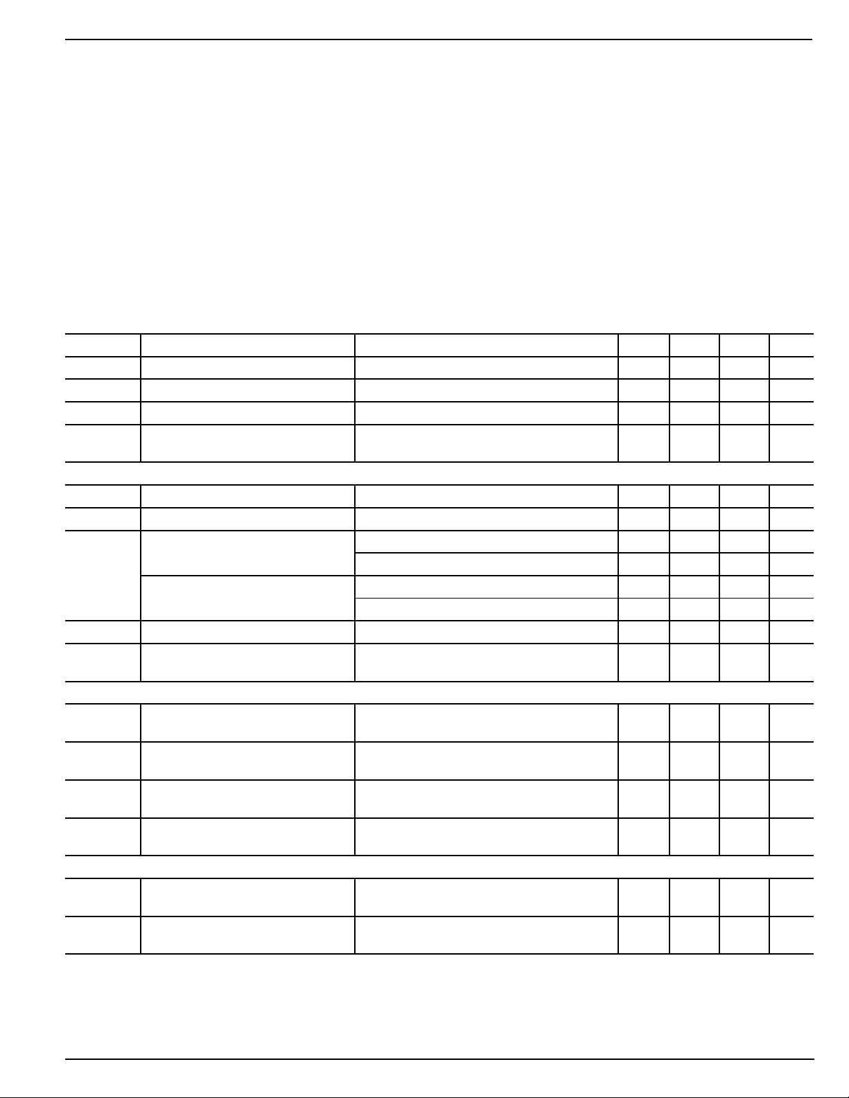
Absolute Maximum Ratings (Note 1)
Supply Voltage ...........................................................+22V
Input Voltage ................................. VS + 0.3V to GND – 5V
Junction Temperature .............................................. 150°C
Storage Temperature Range .................... –65°C to 150°C
Lead Temperature (10 sec.)..................................... 300°C
ESD Susceptability, Note 3...................................... 1000V
Operating Ratings (Note 2)
Supply Voltage (VS) .................................... +4.5V to +18V
Temperature Range
C Version .................................................. 0°C to +70°C
B Version............................................... –40°C to +85°C
Package Thermal Resistance
DIP θJA............................................................. 130°C/W
DIP θJC............................................................... 42°C/W
Wide-SOIC θJA................................................. 120°C/W
Wide-SOIC θJC................................................... 75°C/W
SOIC θJA.......................................................... 120°C/W
SOIC θJC............................................................ 75°C/W
MIC4423/4424/4425 Electrical Characteristics
4.5V ≤ VS ≤ 18V; TA = 25°C, bold values indicate –40°C ≤ TA ≤ +85°C; unless noted.
Symbol Parameter Conditions Min Typ Max Units
Input
V
IH
V
IL
I
IN
Output
V
OH
V
OL
R
O
I
PK
I Latch-Up Protection >500 mA
Switching Time (Note 4)
t
R
t
F
t
D1
t
D2
Power Supply
I
S
I
S
Logic 1 Input Voltage 2.4 V
Logic 0 Input Voltage 0.8 V
Input Current 0V ≤ VIN ≤ V
S
–1 1 µA
–10 10 µA
High Output Voltage
VS–0.025
V
Low Output Voltage 0.025 V
Output Resistance HI State I
Output Resistance LO State I
= 10mA, VS = 18V 2.8 5 Ω
OUT
VIN = 0.8V, I
= 10mA, VS = 18V 3.5 5 Ω
OUT
VIN = 2.4V, I
= 10mA, VS = 18V 3.7 8 Ω
OUT
= 10mA, VS = 18V 4.3 8 Ω
OUT
Peak Output Current 3A
Withstand Reverse Current
Rise Time test Figure 1, CL = 1800pF 23 35 ns
28 60 ns
Fall Time test Figure 1, CL = 1800pF 25 35 ns
32 60 ns
Delay Tlme test Ffigure 1, CL = 1800pF 33 75 ns
32 100 ns
Delay Time test Figure 1, CL = 1800pF 38 75 ns
38 100 ns
Power Supply Current VIN = 3.0V (both inputs) 1.5 2.5 mA
2 3.5 mA
Power Supply Current VIN = 0.0V (both inputs) 0.15 0.25 mA
0.2 0.3 mA
Note 1. Exceeding the absolute maximum rating may damage the device.
Note 2. The device is not guaranteed to function outside its operating rating.
Note 3. Devices are ESD sensitive. Handling precautions recommended. ESD tested to human body model, 1.5k in series with 100pF.
Note 4. Switching times guaranteed by design.
January 1999 3 MIC4423/4424/4425
MIC4423/4424/4425 Micrel
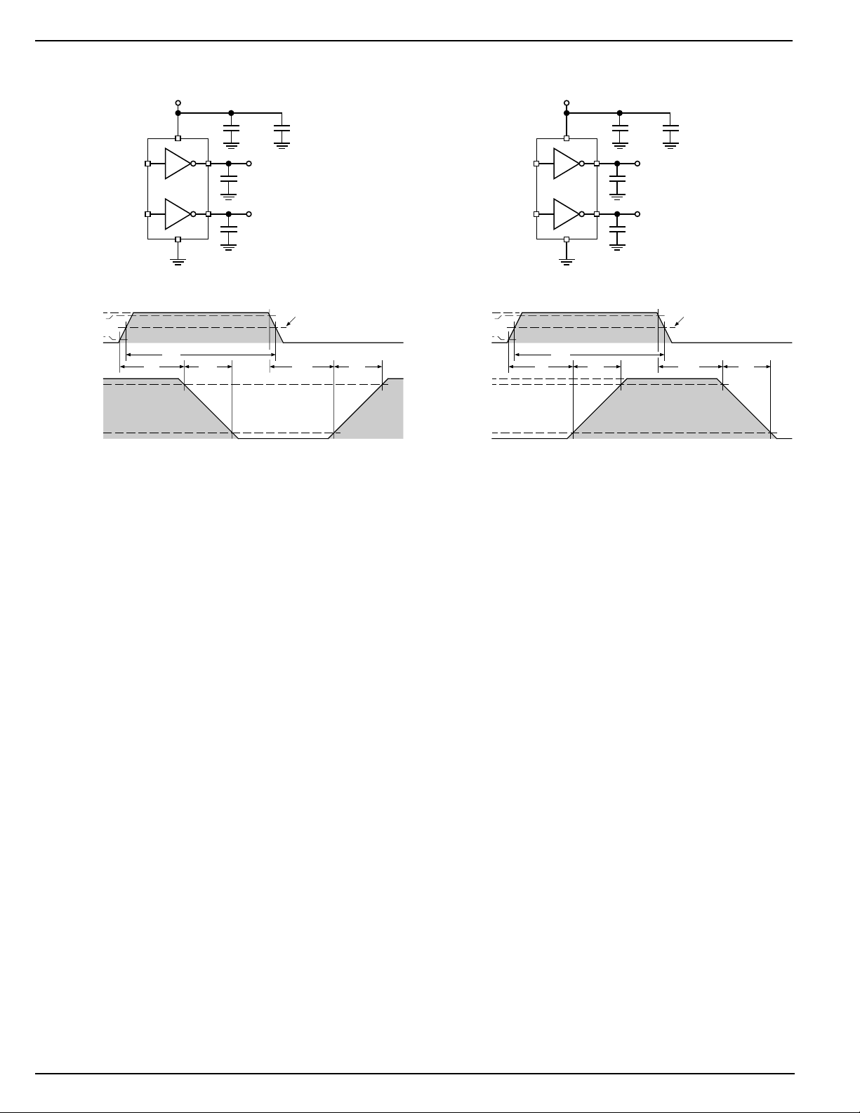
Test Circuit
INPUT
OUTPUT
VS = 18V
0.1µF 4.7µF
OUTA
1800pF
OUTB
1800pF
2.5V
t
D2
t
PW
≥ 0.5µs
5V
90%
10%
0V
V
90%
MIC4423
t
D1
A
B
t
PW
t
F
INA
INB
S
10%
0V
Figure 1a. Inverting Driver Switching Time
VS = 18V
0.1µF 4.7µF
INA
INB
A
MIC4424
B
5V
90%
INPUT
10%
0V
t
R
V
90%
S
t
PW
t
D1
t
R
OUTA
1800pF
OUTB
1800pF
2.5V
t
D2
t
PW
≥ 0.5µs
t
F
OUTPUT
10%
0V
Figure 1b. Noninverting Driver Switching Time
MIC4423/4424/4425 4 January 1999