

MICREL MIC4416BM4, MIC4417BM4 Datasheet
MIC4416 Micrel
MIC4416/4417
IttyBitty™ Low-Side MOSFET Driver
General Description
The MIC4416 and MIC4417 IttyBitty™ low-side MOSFET
drivers are designed to switch an N-channel enhancementtype MOSFET from a TTL-compatible control signal in lowside switch applications. The MIC4416 is noninverting and
the MIC4417 is inverting. These drivers feature short delays
and high peak current to produce precise edges and rapid
rise and fall times. Their tiny 4-lead SOT-143 package uses
minimum space.
The MIC4416/7 is powered from a +4.5V to +18V supply
voltage. The on-state gate drive output voltage is approximately equal to the supply voltage (no internal regulators or
clamps). High supply voltages, such as 10V, are appropriate
for use with standard N-channel MOSFETs. Low supply
voltages, such as 5V, are appropriate for use with logic-level
N-channel MOSFETs.
In a low-side configuration, the driver can control a MOSFET
that switches any voltage up to the rating of the MOSFET.
The MIC4416 is available in the SOT-143 package and
is rated for –40°C to +85°C ambient temperature range.
Features
• +4.5V to +18V operation
• Low steady-state supply current
50µA typical, control input low
370µA typical, control input high
• 1.2A nominal peak output
3.5Ω typical output resistance at 18V supply
7.8Ω typical output resistance at 5V supply
• 25mV maximum output offset from supply or ground
• Operates in low-side switch circuits
• TTL-compatible input withstands –20V
• ESD protection
• Inverting and noninverting versions
Applications
• Battery conservation
• Solenoid and motion control
• Lamp control
• Switch-mode power supplies
Ordering Information
Part Number Temp. Range Package Marking
Noninverting
MIC4416BM4 –40°C to +85°C SOT-143 D10
Inverting
MIC4417BM4 –40°C to +85°C SOT-143 D11
5
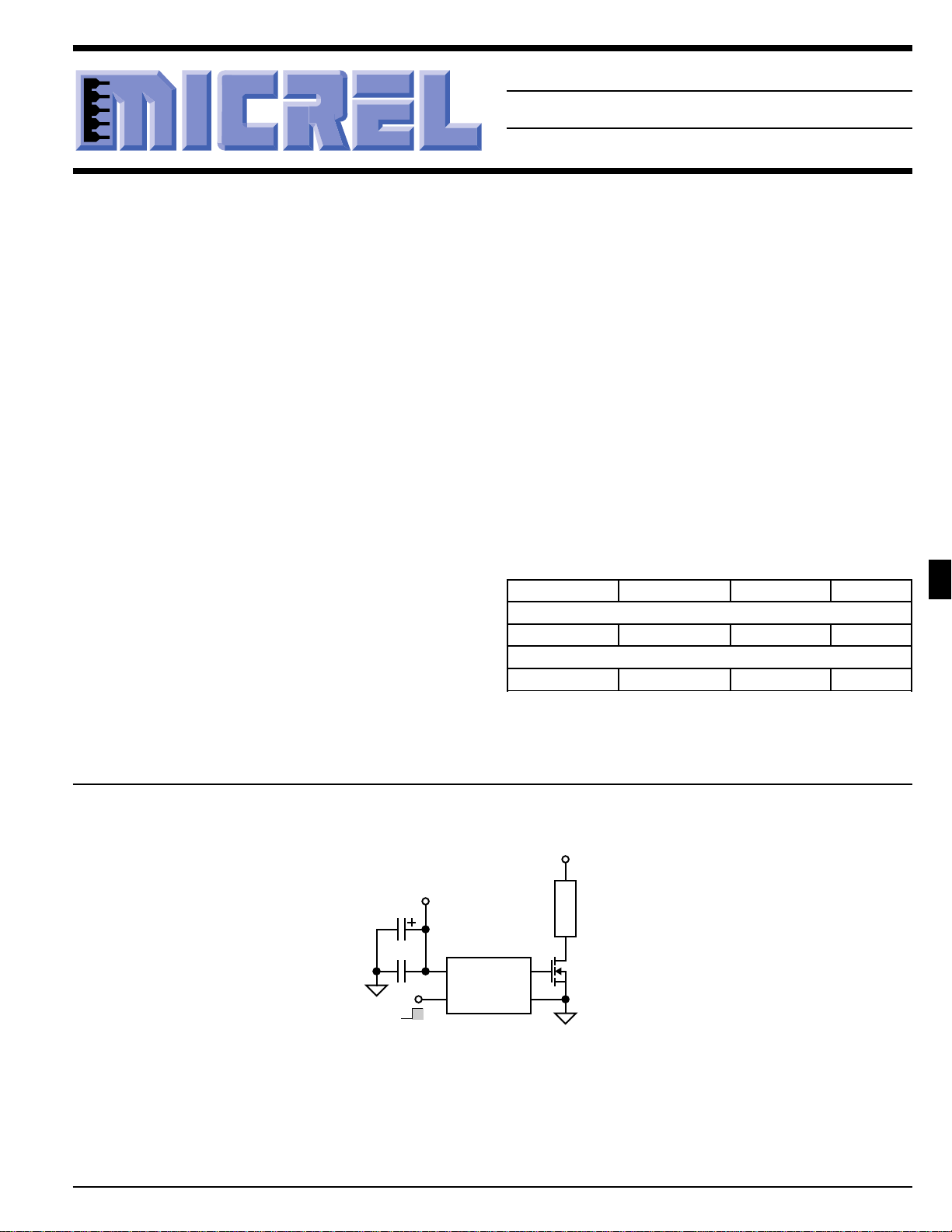
Typical Application
* Siliconix
30m
Ω
, 7A max.
†
Load voltage limited only by
MOSFET drain-to-source rating
+12V
4.7µF
0.1µF
On
Off
Low-Side Power Switch
April 1998 5-23
MIC4416
32
VS
4
CTLGGND
Load
Voltage
1
†
Load
Si9410DY*
N-channel
MOSFET
MIC4416 Micrel
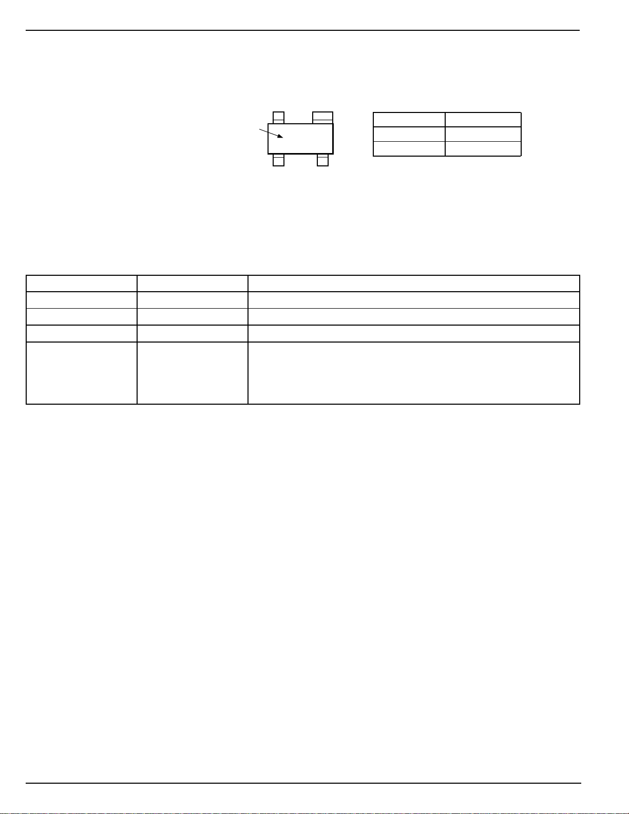
Pin Configuration
Identification
Part
Pin Description
Pin Number Pin Name Pin Function
1 GND Ground: Power return.
2 G Gate (Output) : Gate connection to external MOSFET.
3 VS Supply (Input): +4.5V to +18V supply.
4 CTL Control (Input): TTL-compatible on/off control input.
Dxx
GND
12
CTLVS
Part Number Identification
MIC4416BM4 D10
MIC4417BM4 D11
Early production identification: ML10
G
34
SOT-143 (M4)
MIC4416 only:
Logic low forces the gate output to ground.
MIC4417 only:
forces the gate output to the supply voltage.
Logic high forces the gate output to the supply voltage.
Logic high forces the gate output to ground. Logic low
5-24 April 1998
MIC4416 Micrel
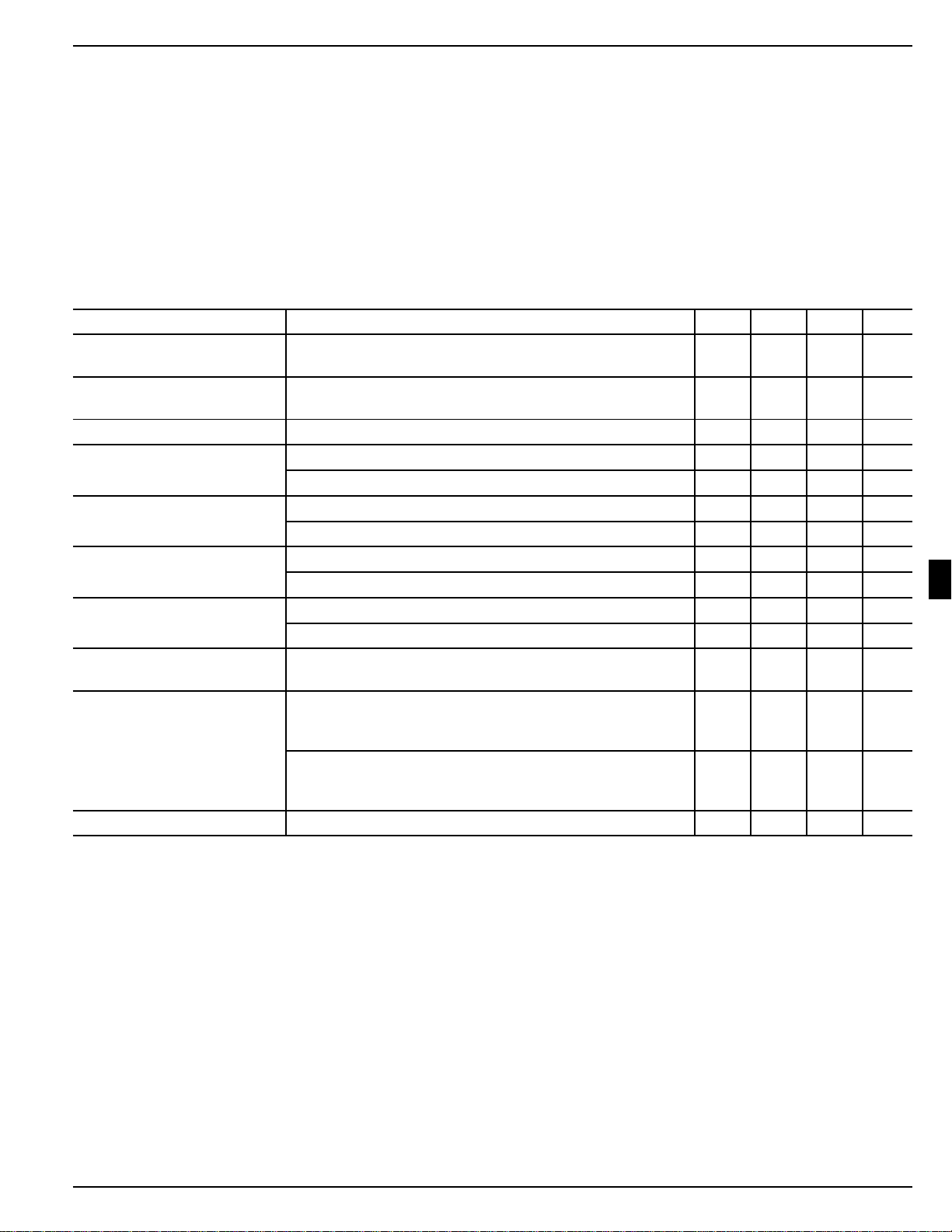
Absolute Maximum Ratings
Supply Voltage (VS) ....................................................+20V
Control Voltage (V
Gate Voltage (VG) .......................................................+20V
Junction Temperature (TJ) ........................................ 150°C
) .................................. –20V to +20V
CTL
Operating Ratings
Supply Voltage (VS) ....................................... +4.5 to +18V
Ambient Temperature Range (TA) ............. –40°C to +85°C
Thermal Resistance (θJA)......................................220°C/W
(soldered to 0.25in2 copper ground plane)
Lead Temperature, Soldering ................... 260°C for 5 sec.
Electrical Characteristics
Parameter Condition (Note 1) Min Typ Max Units
Supply Current 4.5V ≤ V
Control Input Voltage 4.5V ≤ V
Control Input Current 0V ≤ V
Delay Time, V
Delay Time, V
Output Rise Time VS = 5V CL = 1000pF, Note 2 24 ns
Output Fall Time VS = 5V CL = 1000pF, Note 2 28 ns
Gate Output Offset Voltage 4.5V ≤ V
Output Resistance V
Gate Output Reverse Current No latch up 250 mA
Rising VS = 5V CL = 1000pF, Note 2 42 ns
CTL
VS = 18V CL = 1000pF, Note 2 33 60 ns
Falling VS = 5V CL = 1000pF, Note 2 42 ns
CTL
VS = 18V CL = 1000pF, Note 2 23 40 ns
VS = 18V CL = 1000pF, Note 2 14 40 ns
VS = 18V CL = 1000pF, Note 2 16 40 ns
S
V
S
≤ 18V V
S
≤ 18V V
S
≤ V
CTL
S
≤ 18V VG = high –25 mV
S
= 5V, I
= 18V, I
OUT
OUT
= 10mA
= 10mA
= 0V 50 200 µA
CTL
V
= 5V 370 1500 µA
CTL
for logic 0 input 0.8 V
CTL
V
for logic 1 input 2.4 V
CTL
–10 10 µA
VG = low 25 mV
P-channel (source) MOSFET 7.6 Ω
N-channel (sink) MOSFET 7.8 Ω
P-channel (source) MOSFET 3.5 10 Ω
N-channel (sink) MOSFET 3.5 10 Ω
5
General Note: Devices are ESD protected, however handling precautions are recommended.
Note 1: Typical values at TA = 25°C. Minimum and maximum values indicate performance at –40°C ≥ TA ≥ +85°C. Parts production tested at 25°C.
Note 2: Refer to “MIC4416 Timing Definitions” and “MIC4417 Timing Definitions” diagrams (see next page).
April 1998 5-25
 Loading...