

MICREL MIC29510-5.0BT, MIC29510-3.3BT, MIC29512BT Datasheet

MIC29510/29512 Micrel
MIC29510/29512
5A Fast-Response LDO Regulator
Preliminary Information
General Description
The MIC29510 and MIC29512 are high-current, high-accuracy, low-dropout voltage regulators featuring fast transient
recovery from input voltage surges and output load current
changes. These regulators use a PNP pass element that
features Micrel’s proprietary Super ßeta PNP™ process.
The MIC29510/2 is available in two versions: the three pin
fixed output MIC29510 and the five pin adjustable output
voltage MIC29512. All versions are fully protected against
overcurrent faults, reversed input polarity, reversed lead
insertion, overtemperature operation, and positive and negative transient voltage spikes.
A TTL compatible enable (EN) control pin supports external
on/off control. If on/off control is not required, the device may
be continuously enabled by connecting EN to IN.
The MIC29510/2 is available in the standard three and five
pin TO-220 package with an operating junction temperature
range of 0°C to +125°C.
For applications requiring even lower dropout voltage, input
voltage greater than 16V, or an error flag, see the MIC29500/
29501/29502/29503.
Ordering Information
Features
• Fast transient response
• 5A current capability
• 700mV dropout voltage at full load
• Low ground current
• Accurate 1% guaranteed tolerance
• “Zero” current shutdown mode (MIC29512)
• Fixed voltage and adjustable versions
Applications
• Pentium™ and Power PC™ processor supplies
• High-efficiency “green” computer systems
• High-efficiency linear power supplies
• High-efficiency switching supply post regulator
• Battery-powered equipment
T ypical Application
MIC29510
V
IN
IN
GND
Fixed Regulator Configuration
OUT
Part Number Temp. Range* Voltage Current Package
MIC29510-3.3BT 0°C to +125°C 3.3V 5.0A TO-220-3
MIC29510-5.0BT 0°C to +125°C 5.0V 5.0A TO-220-3
MIC29512BT 0°C to +125°C Adj. 5.0A TO-220-5
* Junction Temperature
MIC29512
V
OUT
On
Off
V
IN
EN
IN
V
OUT
GND
= 1.240
OUT
ADJ
R1
R2
R1
R2
+ 1
V
Adjustable Regulator Configuration
OUT
3-96 1997
MIC29510/29512 Micrel
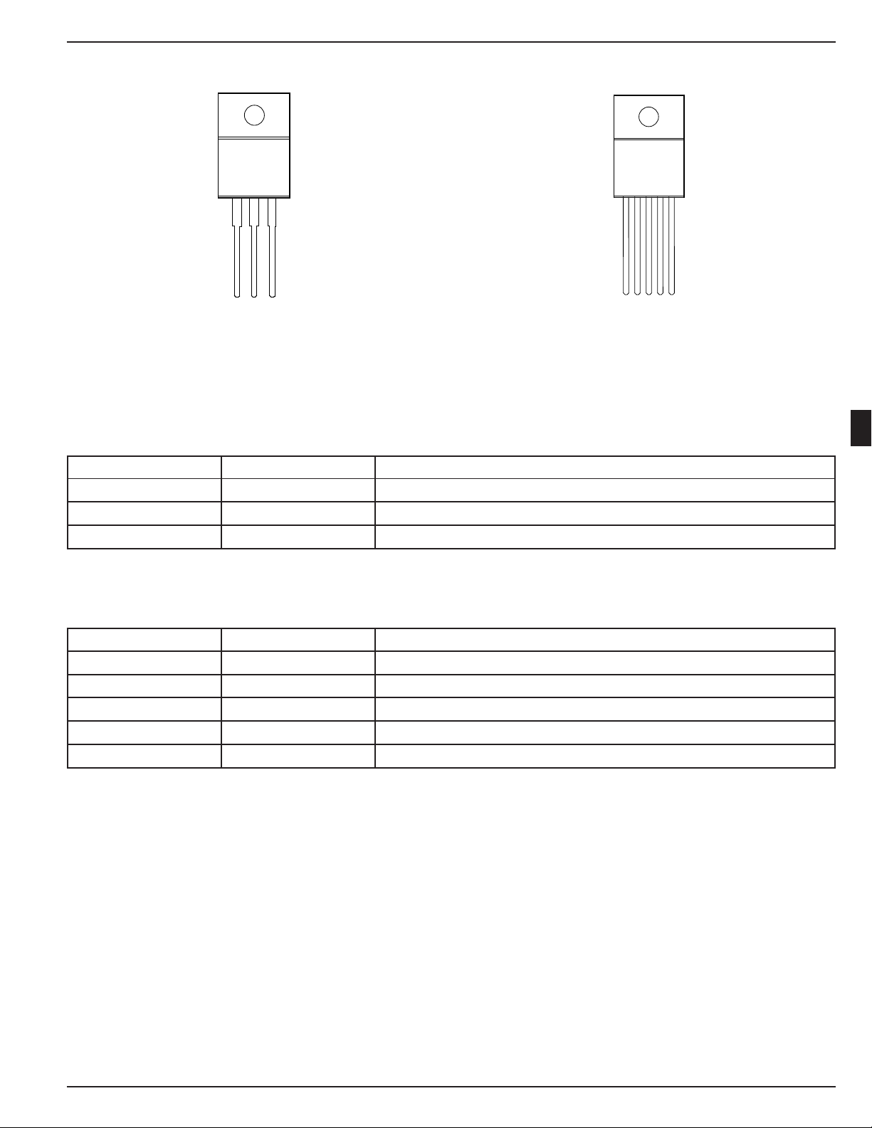
Pin Configuration
1 2 3
MIC29510BT
On all devices, the Tab is grounded.
Pin Description
3-Pin TO-220 (MIC29510)
Pin Number Pin Name Pin Function
1 IN Unregulated Input: +16V maximum supply.
2 GND Ground: Internally connected to tab (ground).
3 OUT Regulated Output
5-Pin TO-220 (MIC29512)
Pin Number Pin Name Pin Function
1 EN Enable (Input): Logic-level ON/OFF control.
2 IN Unregulated Input: +16V maximum supply.
3 GND Ground: Internally connected to tab (ground).
4 OUT Regulated Output
5 ADJ Output Voltage Adjust: 1.240V feedback from external resistive divider.
12345
MIC29512BT
3
Absolute Maximum Ratings
Input Supply Voltage (Note 1) ....................... –20V to +20V
Power Dissipation .................................... Internally Limited
Storage Temperature Range ................... –65°C to +150°C
Lead Temperature (Soldering, 5 sec.) ...................... 260°C
1997 3-97
Operating Ratings
Operating Junction Temperature ................. 0°C to +125°C
θJC (TO-220) .............................................................2°C/W
θJA (TO-220) ...........................................................55°C/W
MIC29510/29512 Micrel
Electrical Characteristics
All measurements at TJ = 25°C unless otherwise noted. Bold values are guaranteed across the operating temperature range.
Parameter Condition Min Typ Max Units
Output Voltage 10mA ≤ IO ≤ IFL, (V
Line Regulation IO = 10mA, (V
Load Regulation VIN = V
OUT
+ 1V, 10mA ≤ I
OUT
∆VO / ∆T Output VoltageTemperature Coefficient (Note 6) 20 100 ppm/°C
Dropout Voltage ∆V
= – 1%, (Note 3)
OUT
MIC29510/29512 I
Ground Current MIC29510/29512 I
Ground Pin VIN = 0.5V less than specified V
I
GNDDO
Current at Dropout
Current Limit MIC29510/29512 V
, Output Noise Voltage CL = 47µF 260 µV
e
n
(10Hz to 100kHz) IL = 100mA
+ 1V) ≤ VIN ≤ 8V (Note 2) –2 2 %
OUT
+ 1V) ≤ VIN ≤ 8V 0.06 0.5 %
≤ I
OUT
FULL LOAD
= 100mA 80 200 mV
O
= 750mA 200 mV
I
O
I
= 1.5A 320 mV
O
= 3A 500 mV
I
O
(Notes 2, 6) 0.2 1 %
IO = 5A 700 1000 mV
= 750mA, VIN = V
O
= 1.5A 10 mA
I
O
= 3A 36 mA
I
O
IO = 5A 100 150 mA
OUT
= 0V (Note 4) 5.0 6.5 A
OUT
+ 1V 3 20 mA
OUT
. I
= 10mA 2 3 mA
OUT
RMS
Reference (MIC29512 only)
Reference Voltage 10mA ≤ IO ≤ IFL, V
+ 1V ≤ VIN ≤ 8V (Note 2) 1.215 1.265 V
OUT
MAX
Adjust Pin Bias Current 40 80 nA
120 nA
Reference Voltage (Note 7) 20 ppm/°C
Temperature Coefficient
Adjust Pin Bias Current 0.1 nA/°C
Temperature Coefficient
3-98 1997
 Loading...