

MICREL MIC2755BMM Datasheet
MIC2755 Micrel
MIC2755
Battery System Supervisor
Preliminary Information
General Description
The MIC2755 is composed of multiple comparators, a reset
pulse generator, and logic. It is designed for monitoring the
battery supply of portable digital systems, including PDAs
and pagers.
The MIC2755 detects three different battery states: battery
OK, low battery, and dead battery. The reset (/RST) output is
asserted for at least 700ms when a fresh battery is inserted.
The nonmaskable interrupt output (/NMI) is asserted when
the battery voltage is below the NTH threshold, indicating that
high-power system operations should not occur. If and when
battery voltage falls below the power-off threshold (PTH), the
reset output is asserted and latched, inhibiting system operation until the battery is replaced or recharged.
All three voltage thresholds are set using external resistors.
A manual reset function can be implemented by connecting
a switch directly to the power on reset/manual reset [RTH(/MR)]
input. Internal circuitry detects switch activation and generates a minimum 175ms debounced reset signal. The
MIC2755’s power supply input is separate from the detector
inputs to allow it to be powered from a down-stream voltage,
such as the output of a boost converter.
Inputs and outputs can be pulled above V
absolute maximum) without adverse effects or excessive
current draw.
Supply current is typically a low 2µA. Hysteresis is included
on all voltage detectors to prevent chattering due to noise.
The MIC2755 is available in the tiny 8-lead micro-smalloutline package.
(up to 7V
DD
Features
• Optimized for PDAs, pagers and
other hand-held devices.
• Detects multiple battery states:
- battery OK
- low battery
- dead battery
• Adjustable voltage thresholds
• High accuracy ±2% voltage thresholds
• Reset generation at power-on (700ms min.)
• Debounced manual reset function
• Internal logic prevents chatter if battery voltage
fluctuates
• Extremely low 2µA typical supply current
• I/Os can be pulled above VDD (7V absolute maximum)
• Immune to brief power supply transients
• Low cost
• 8-lead MSOP
Applications
• PDAs
• Pagers
• Consumer electronics
• Embedded controllers
• Portable instruments
• Data loggers
Ordering Information
Part Number Junction Temp. Range Package
MIC2755BMM –40°C to +85°C 8-pin MSOP
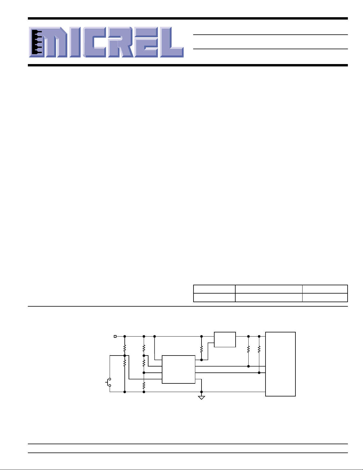
Typical Application
Boost or Buck
Converter
IN OUT
EN
V
BAT(OK)
V
BAT(low)
V
BAT(dead)
= 3.6V
= 3.1V
= 2.9V
SW
RESET
V
656k
344k
BAT
576k
26.7k
400k
MIC2755
VDD /POF
PTH
NTH
RTH(/MR)
/NMI
/RST
GND
100k 100k 100k
Supervised Boost Converter and Microcontroller or Microprocessor
Micrel, Inc. • 1849 Fortune Drive • San Jose, CA 95131 • USA • tel + 1 (408) 944-0800 • fax + 1 (408) 944-0970 • http://www.micrel.com
February 2000 1 MIC2755
µController or
µProcessor
SUPPLY
/NMI
/RST
GND
MIC2755 Micrel
Pin Configuration
NTH
PTH
GND
Pin Description
Pin Number Pin Name Pin Function
1 RTH(/MR) Power-On Reset Threshold (Analog Input): Comparator input assigned to
2 NTH Nonmaskable Interrupt Threshold (Analog Input): Voltage monitor input
3 PTH Power-Off Threshold (Analog Input): Voltage monitor input assigned to
4 GND Ground: Power and signal return for all IC functions.
5 /POF Power-off (Output): Active-low, open-drain output. Asserted and latched
6 /NMI Nonmaskable Interrupt (Output): Active-low, open-drain output. Asserted
7 /RST Reset (Output): Active-low, open-drain output. Asserted for a minimum of
8 VDD (Analog Input): Power supply input.
1RTH(/MR)
2
3
4
8 VDD
/RST
7
/NMI
6
/POF
5
8-Lead MSOP (MM)
battery-OK condition detection. When the level on this pin first exceeds
, the reset generator cycles. The /RST output is held low for a minimum
V
REF
of 700ms and the /POF threshold output is deasserted.
assigned to “low battery” condition detection. When the level on this pin falls
below V
“dead battery” condition detection. When the level on this pin falls below
V
REF
a reset cycle occurs (V
when V
in reset until the battery is replaced and a power-on reset cycle occurs.
when V
power system operation should not be allowed.
700ms at power-on or anytime V
175ms minimum when RTH (/MR) is externally pulled low (manual reset).
, the /NMI output is asserted.
REF
, the /RST and /POF outputs are asserted. The condition is latched until
PTH
NTH
< V
< V
> V
RTH
, which is a “dead battery” condition. The system is held
REF
, which is a “low battery” condition. This indicates high-
REF
).
REF
drops below V
PTH
. Also asserted for
REF
MIC2755 2 February 2000

MIC2755 Micrel
Absolute Maximum Ratings (Note 1)
Supply Voltage (V
Input Voltage (V
Output Voltage (V
/RST Output Current (I
Storage Temperature (T
ESD Rating, Note 3 ......................................................2kV
) ..................................... –0.3V to +7V
DD
RTH
/RST
), (V
), (V
NTH
), (V
/NMI
) .......................................20mA
/RST
) ....................... –65°C to +150°C
S
) ............. –0.3V to +7V
PTH
), (V
) ........ –0.3V to +7V
/POF
Operating Ratings (Note 2)
Supply Voltage (V
Input Voltage (V
Output Voltage (V
Ambient Temperature Range (TA) ............. –40°C to +85°C
Package Thermal Resistance
1-layer PCB (θ
) .................................. +1.5V to +5.5V
DD
), (V
RTH
/RST
) ..............................................206°C/W
JA
NTH
), (V
), (V
/NMI
) ............. –0.3V to +6V
PTH
), (V
) ........ –0.3V to +6V
/POF
4-layer PCB (θJA) ..............................................113°C/W
Electrical Characteristics
VDD = 3.3V; TA = 25°C, bold values indicate –40°C ≤ TA ≤ +85°C; unless noted
Symbol Parameter Condition Min Typ Max Units
I
DD
I
RTH(/MR)
, I
I
NTH
PTH
I
/RST, I/NMI
I
/POF
V
REF1
V
REF2
V
HYST
Reset Output (/RST)
t
/RST
t
/MR
V
/RST
Reset Input [RTH(/MR)]
V
/MRTV
t
DBNC
t
PROP
Nonmaskable Interrupt Output (/NMI)
t
PROP
V
/NMI
Power-Off Output (/POF)
t
PROP
V
/POF
Note 1. Exceeding the absolute maximum rating may damage the device.
Note 2. The device is not guaranteed to function outside its operating rating.
Note 3. Devices are ESD sensitive. Handling precautions recommended. Human body model, 100pF in series with 1.5k .
Note 4. VDD operating range is 1.5V to 5.5V. Output is guaranteed to be held low down to VDD = 1.2V.
Note 5.
Operating Supply Current outputs open, V
outputs open, V
RTH
RTH
, V
, V
NTH
NTH
, V
> 1.24V 2.0 4.0 µA
PTH
, V
< 1.24V 1.7 µA
PTH
, Leakage Current 5pA
, 10 nA
,
Threshold Voltage for RTH(/MR) and PTH inputs 1.215 1.240 1.265 V
Threshold Voltage for NTH inputs 1.215 1.240 1.265 V
Hysteresis Voltage on NTH 20 mV
Comparator
Reset Pulse Width 700 1200 ms
Manual Reset Pulse Width 175 300 ms
/RST Output Voltage Low, Note 4 /RST asserted, I
/RST asserted, I
= 1.6mA, VDD ≥ 1.6V 0.3 V
SINK
= 100µA, VDD ≥ 1.2V 0.4 V
SINK
Manual Reset Trip Voltage 275 310 345 mV
Debounce Time V
/MRTV(min)
Propogation Delay from (V
to RST Asserted
Propagation Delay (V
REF(max)
< V
RTH
< V
/MR
RTH(/MR)(min)
+ 100mV) < V
< V
/MRTV(max)
, Note 5 22 38 ms
– 100mV) 9 µs
NTH
< (V
REF(min)
9 µs
– 100mV)
/NMI Output Voltage Low /NMI asserted, I
/NMI asserted, I
Propagation Delay (V
– 100mV)
/POF Output Voltage Low /POF asserted, I
/POF asserted, I
t
t
t
DBNC
/RST /MR
==
32
8
. These relationships are guaranteed by design.
REF(max)
+ 100mV) < V
= 1.6mA, VDD ≥ 1.6V 0.3 V
SINK
= 100µA, VDD ≥ 1.2V 0.4 V
SINK
< (V
PTH
= 1.6mA, VDD ≥ 1.6V 0.3 V
SINK
= 100µA, VDD ≥ 1.2V 0.4 V
SINK
REF(min)
9 µs
February 2000 3 MIC2755
MIC2755 Micrel
Timing Diagram
V
V
V
BAT
V
V
/MR
/RST
/NMI
/POF
V
V
V
V
V
V
V
/MRH
/MRL
/RSTH
/RSTL
/NMIH
/NMIL
/POFH
/POFL
V
V
V
V
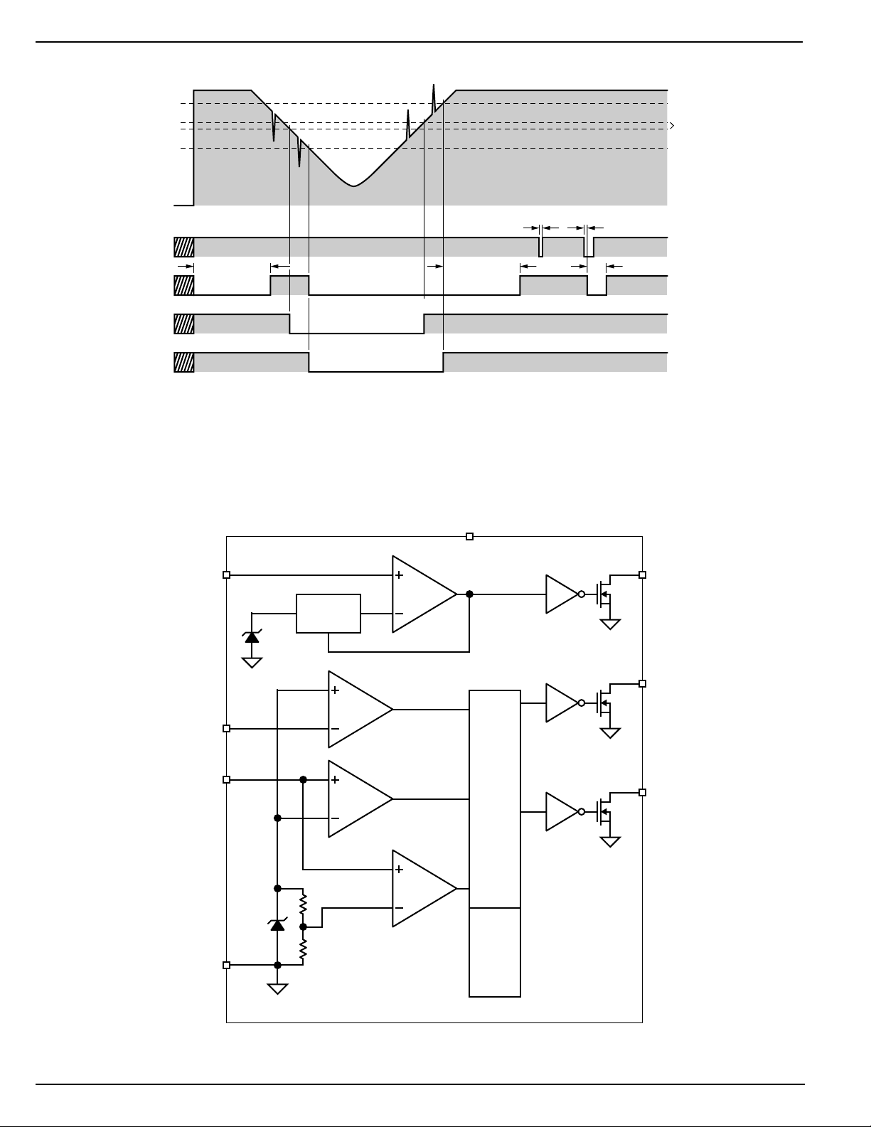
Block Diagram
PTH
0V
RTH
NTH
t
RST
Propagation delays not shown for clarity.
The MIC2755 ignores very brief transients. See “Application
Information” for details.
t
RST
<t
DBNC
>t
DBNC
t
/MR
NOT TO SCALE.
20mV
V
EXPANDED
BAT
VERTICALLY TO
SHOW DETAIL.
NTH
PTH
RTH(/MR)
1.24V
Ref1
1.24V
Ref2
20mV
Hysteresis
310mV
VDD
Machine
Logic-State
/NMI
/RST
/POF
GND
Oscillator
MIC2755 4 February 2000
 Loading...