

MICREL MIC2564A-0BSM, MIC2564A-0BTS, MIC2564A-1BSM, MIC2564A-1BTS Datasheet
MIC2564A Micrel
MIC2564A
Dual Serial PCMCIA/CardBus Power Controller
Preliminary Information
General Description
The MIC2564A is dual-slot PC Card (PCMCIA) and CardBus
power controller. It is a sophisticated power switching matrix
that controls VCC and VPP voltages to two PC Card slots. The
MIC2564A is used in conjunction with a serial-data output
logic controller using the standard three-wire serial control
data format.
When connected to 3.3V, 5V, and 12V system power supplies, the MIC2564A can switch its VCC outputs between 0V,
3.3V, 5.0V, and high-impedance states and VPP outputs
between 0V, 3.3V, 5V, 12V, and high-impedance states. The
VCC outputs will supply a minimum of 1A current to the socket
and the VPP outputs will supply a minimum of 120mA to the
socket. Voltage rise and fall times are well controlled. The
MIC2564A also features an efficient standby (sleep) mode at
0.3µA typical quiescent current.
12V and 5V supplies are not required for MIC2564A opera-
tion making it possible to omit one or both supplies when they
are not needed by the system. An internal charge pump
supplies the internal bias voltages required for high-performance switching.
The MIC2564A is protected by overtemperature shutdown,
and protects itself and the system with current limiting and
cross-conduction lockout.
The MIC2564A is available in 24-pin SSOP and 24-pin
TSSOP.
Features
• Standard 3-wire serial control data input
• Controls two card slots from one surface mount device
• High-efficiency, low-resistance switches
• 12V supply optional (not required by MIC2564A)
• Current limit and overtemperature shutdown
• Ultralow 1µA-typical standby power consumption
• Cross-conduction lockout (no switching transients)
• Break-before-make switching
• 1A minimum VCC output per slot
• Independent VCC and VPP voltage output (MIC2564A-1)
• 120mA minimum VPP output current per slot
• 24-pin surface-mount SSOP and TSSOP packages
Applications
• PC Card and CardBus power control
• Zoom Video port power control
• Wireless communications
• Bar code data collection systems
• Docking stations (portable and desktop)
• Power supply management
Ordering Information
Part Number Temperature Range Package
MIC2564A-0BSM –40°C to +85°C 24-pin SSOP
MIC2564A-1BSM –40°C to +85°C 24-pin SSOP
MIC2564A-0BTS –40°C to +85°C 24-pin TSSOP
MIC2564A-1BTS –40°C to +85°C 24-pin TSSOP
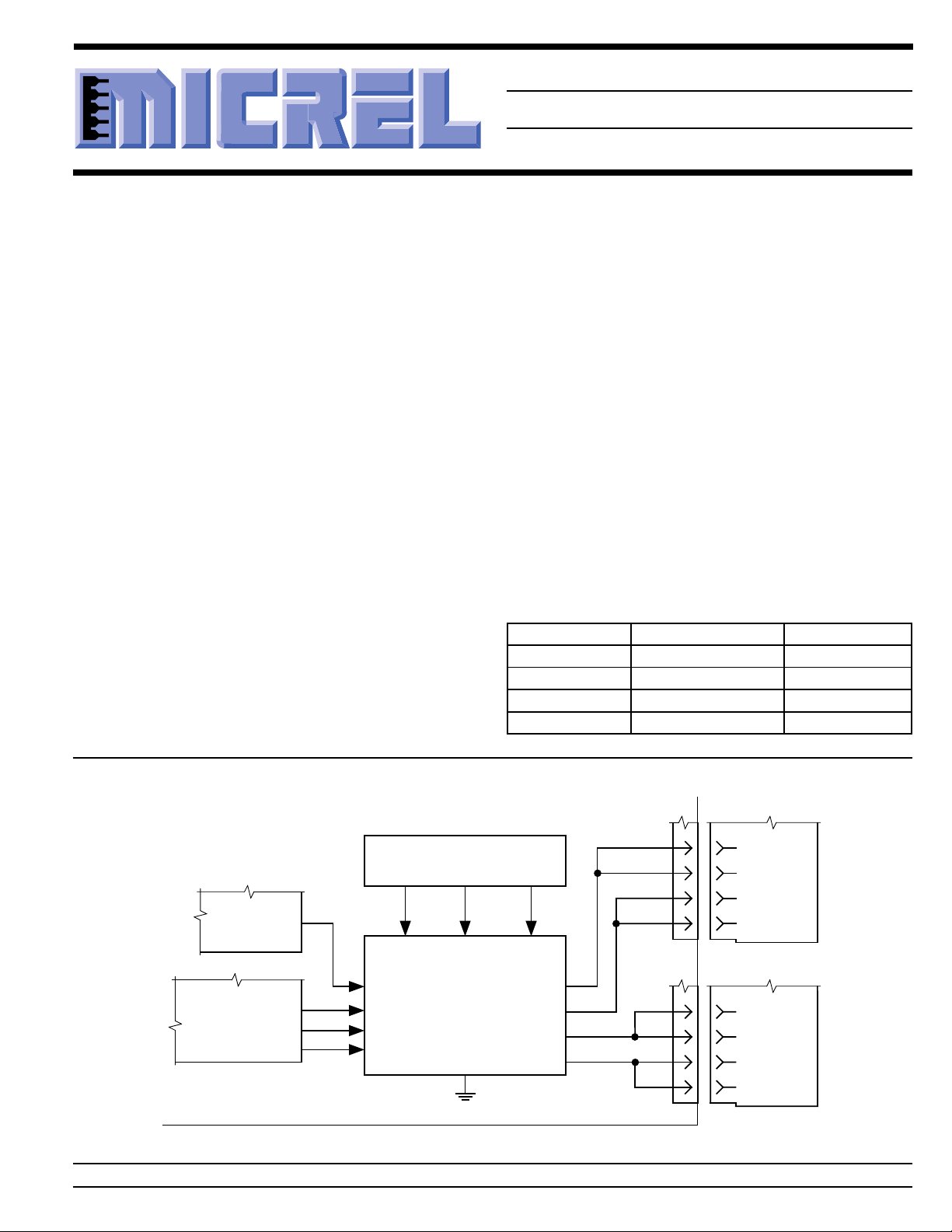
Typical Application
Slot A
Address and data lines
between logic controller and
PCMCIA cards not shown.
System Reset
Dual-Slot
Logic Controller
PCMCIA,
CardBus,
or Zoom Video
System Power Supply
(
OPTIONAL
)
12V
VPP IN
OPTIONAL
(
RST#
Serial
Control
Bus
V
)
MIC2564A
Power
Controller
3.3V
IN V
CC3
GND
OPTIONAL
(
5V
IN
CC5
OPTIONAL
(
A VPP OUT
A V
OUT
CC
B V
OUT
PP
B V
OUT
CC
)
)
Motherboard
PCMCIA Card Power Management Application
Micrel, Inc. • 1849 Fortune Drive • San Jose, CA 95131 • USA • tel + 1 (408) 944-0800 • fax + 1 (408) 944-0970 • http://www.micrel.com
September 1999 1 MIC2564A
V
1
PP
V
2
PP
V
CC
Slot B
1
V
PP
V
2
PP
V
CC
PCMCIA
Card
A
PCMCIA
Card
B
MIC2564A Micrel
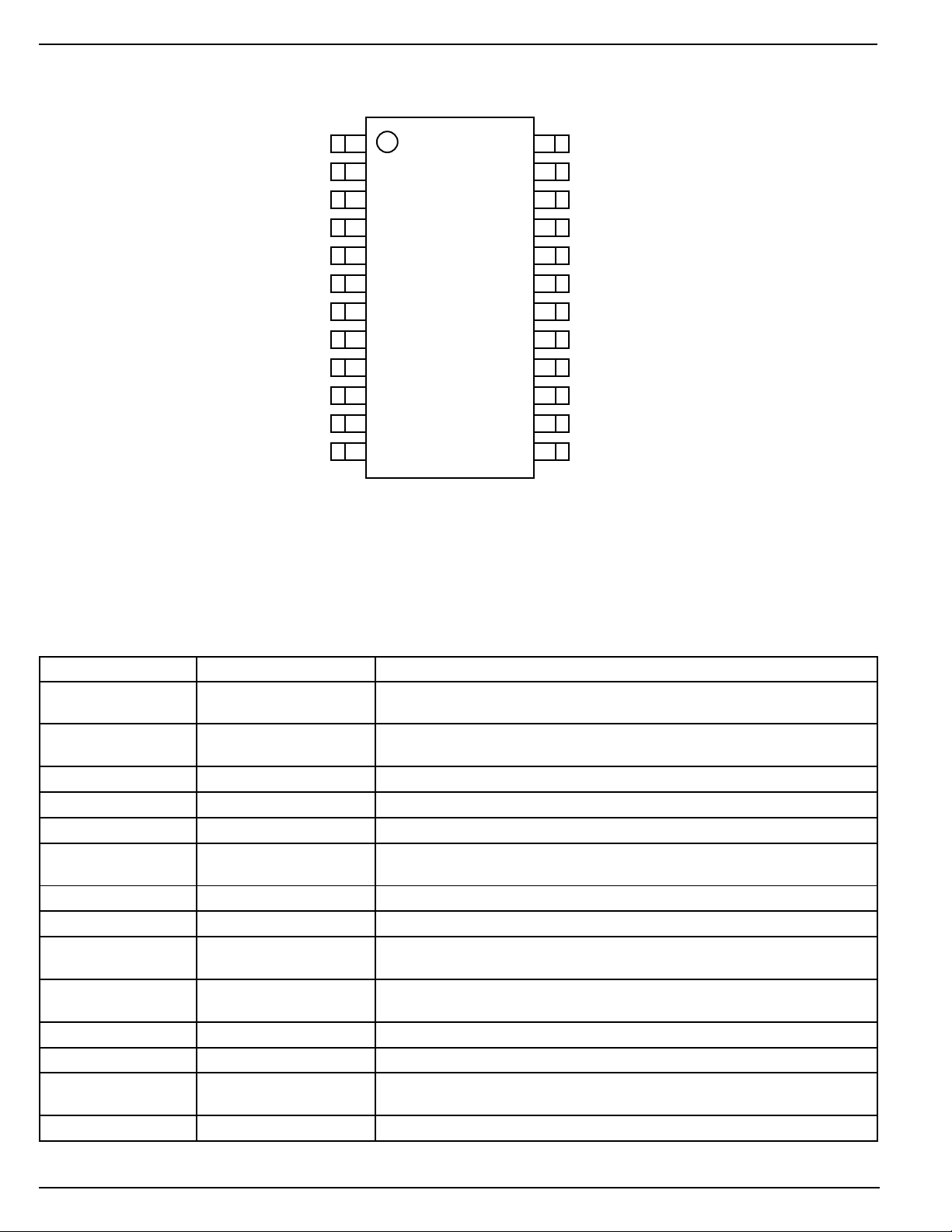
Pin Configuration
1V
CC5
CC5
IN
IN
2A VCC OUT
3V
4A FLAG
A V
V
CC3
A V
GND21
CC
CC
OUT24
IN23
OUT22
5SDA
6SCL
7RST#
8SLA
9B FLAG
10V
IN
CC5
B VCC OUT
V
CC5
11 14
12 13
IN
Pin Description
Pin Number Pin Name Pin Function
1,3,10,12 V
2,22,24 A V
4 A FLAG Channel A VCC and VPP Output Monitor (Output): Low on error condition.
5 SDA Serial Data (Input)
6 SCL Serial Clock (Input)
7 RST# System Reset (Input): Active low signal deactivates the MIC2564A, clearing
8 SLA Serial Data Latch (Input)
9 B FLAG Channel B VCC and VPP Output Monitor (Output): Low on error condition.
11,13,15 B V
14,23 V
16,21 GND Ground
17 B VPP OUT Slot B VPP Output
18,19 V
20 A VPP OUT Slot A VPP Output
IN 5V Supply Input: Optional system power supply connection. Required only
CC5
OUT Slot A VCC Output: Pins 2, 22, and 24 must be externally connected
CC
OUT Slot B VCC Output: Pins 11, 13, and 15 must be externally connected
CC
IN 3.3V Supply Input: Required system power supply connection. Powers 3.3V
CC3
IN 12V Supply Input: Optional system power supply connection. Required only
PP
A V
OUT20
PP
V
IN19
PP
18
17
16
15 B V
V
PP
B V
GND
V
CC3
B V
IN
PP
CC
IN
CC
OUT
OUT
OUT
24-lead SSOP (SM)
24-lead TSSOP (TS)
for 5V VCC and VPP output voltage.
together.
the serial registers and forcing the four power outputs to 0V (GND).
together.
VCC and VPP outputs and all internal circuitry.
for 12V VPP output voltage.
MIC2564A 2 September 1999
MIC2564A Micrel
Absolute Maximum Ratings (Note 1)
VPP IN ......................................................................+13.6V
V
IN.......................................................................+6.0V
CC3
V
IN.......................................................................+6.0V
CC5
V
, V
, V
SCL
VA
FLAG
A or B V
A or B V
SDA
, VB
PP
CC
, V
SLA
.......................................................+6.0V
FLAG
OUT ....................... >120mA, Internally Limited
OUT .............................. >1A, Internally Limited
Power Dissipation at TA ≤ 25°C (PD) .......Internally Limited
Storage Temperature ............................... –65°C to +150°C
Lead Temperature (5 sec.)...................................... +260°C
ESD Rating, Note 3
....................................–0.3V to +6.0V
RST#
Operating Ratings (Note 2)
VPP IN ............................................................ 0V to +13.2V
V
IN........................................................ +3.0V to +5.5V
CC3
V
IN............................................................. 0V to +5.5V
CC5
V
, V
, V
SCL
A or B V
A or B V
SDA
PP
CC
, V
SLA
OUT ................................................0 to 120mA
OUT .......................................................0 to 1A
Clock Frequency .................................................0 to 2MHz
Ambient Temperature (TA).........................–40°C to +85°C
Junction Temperature (TJ) ...................................... +125°C
Package Thermal Resistance (θJA)
SSOP ..............................................................90˚C/W
................................. 0V to +5.5V
RST#
TSSOP ............................................................83˚C/W
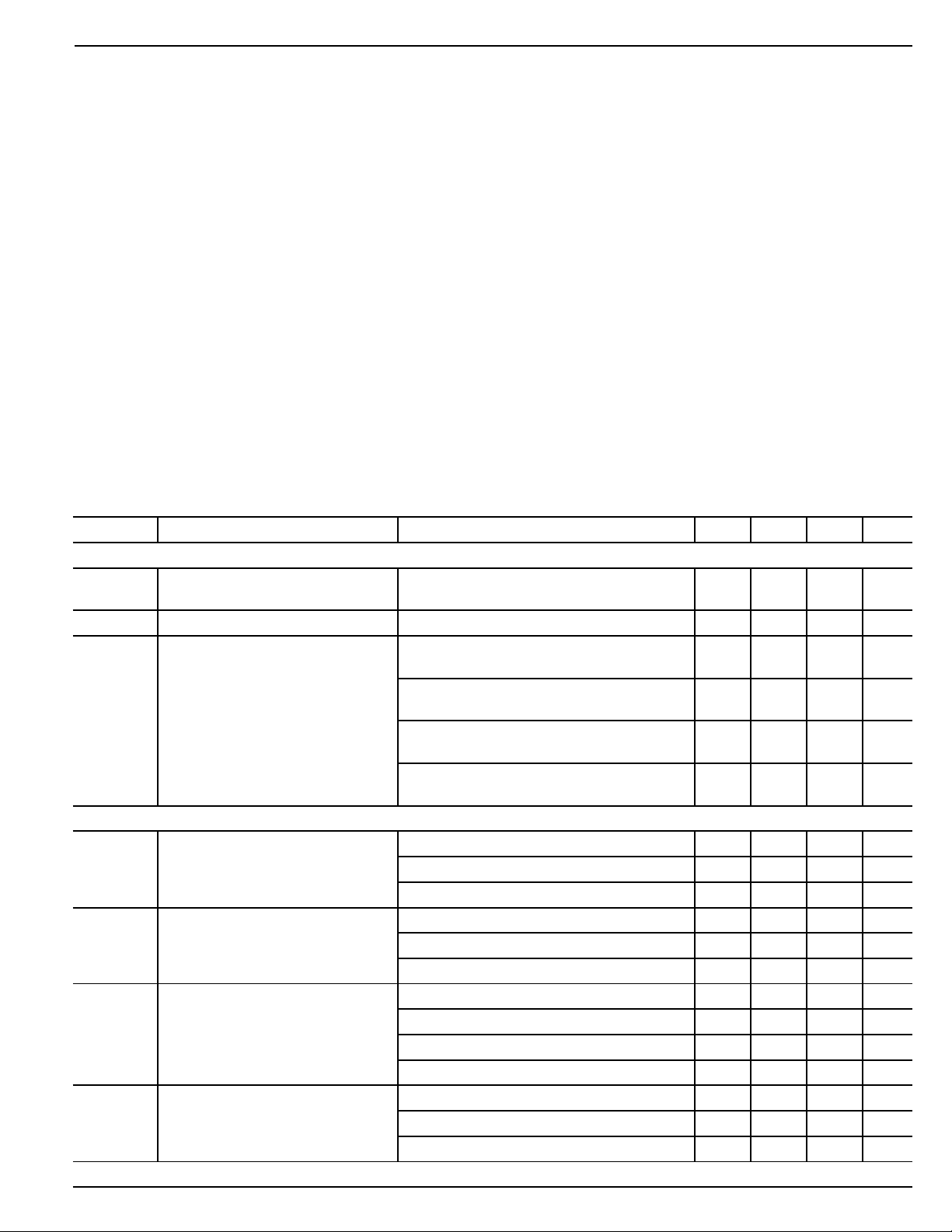
Electrical Characteristics
V
Symbol Parameter Conditions Min Typ Max Units
VPP Output
I
PP
Hi-Z Leakage Current V
I
PPSC
R
VPP Switching Time (See Figure 2)
t
1
t
2
t
3
t
4
t
5
t
6
t
7
t
8
t
9
t
10
t
11
t
12
t
13
CC3 IN
= 3.3V, V
IN = 5.0V, VPP IN = 12V; TA = 25°C, bold indicates –40°C ≤ TA ≤ +85°C; unless noted.
CC5
OUT High Impedance Output shutdown mode 1 10 µA
OUT = 0V
PP
Short Circuit Current Limit V
O
Switch Resistance V
Output Turn-On Delay, Note 5 V
Output Rise Time V
Output Transition Time, Note 5 V
Output Turnoff Fall Time V
OUT = 0V, normal mode, Note 4 120 260 400 mA
PP
OUT = 5V selected, 1.6 5 Ω
PP
I
OUT = –100mA (sourcing)
PP
V
OUT = 3.3V selected, 1.3 5 Ω
PP
I
OUT = –100mA (sourcing)
PP
V
OUT = 12V selected, V
PP
I
OUT = –100 mA (sourcing)
PP
V
OUT = 0V [ground] selected, 2000 5000 Ω
PP
I
OUT = 50µA (sinking)
PP
OUT = Hi-Z to 10% of 3.3V, RL = 100Ω 1 100 µs
PP
V
OUT = Hi-Z to 10% of 5V, RL = 100Ω 1 100 µs
PP
V
OUT = Hi-Z to 10% of 12, RL = 100Ω 50 250 µs
PP
OUT = 10% to 90% of 3.3, RL = 100Ω 10 100 500 µs
PP
V
OUT = 10% to 90% of 5, RL = 100Ω 10 250 1000 µs
PP
V
OUT = 10% to 90% of 12, RL = 100Ω 10 100 500 µs
PP
OUT = 3.3V to 90% of 12V, RL = 100Ω 10 100 500 µs
PP
V
OUT = 5V to 90% of 12, RL = 100Ω 10 100 500 µs
PP
V
OUT = 12V to 90% of 3.3, RL = 100Ω 10 100 500 µs
PP
V
OUT = 12V to 90% of 5, RL = 100Ω 10 250 1000 µs
PP
OUT = 90% to 10% of 3.3, RL = 100Ω 1 500 µs
PP
V
OUT = 90% to 10% of 5, RL = 100Ω 1 500 µs
PP
V
OUT = 90% to 10% of 12, RL = 100Ω 1 500 µs
PP
IN = 12V, 1.3 2.3 Ω
PP
September 1999 3 MIC2564A
MIC2564A Micrel
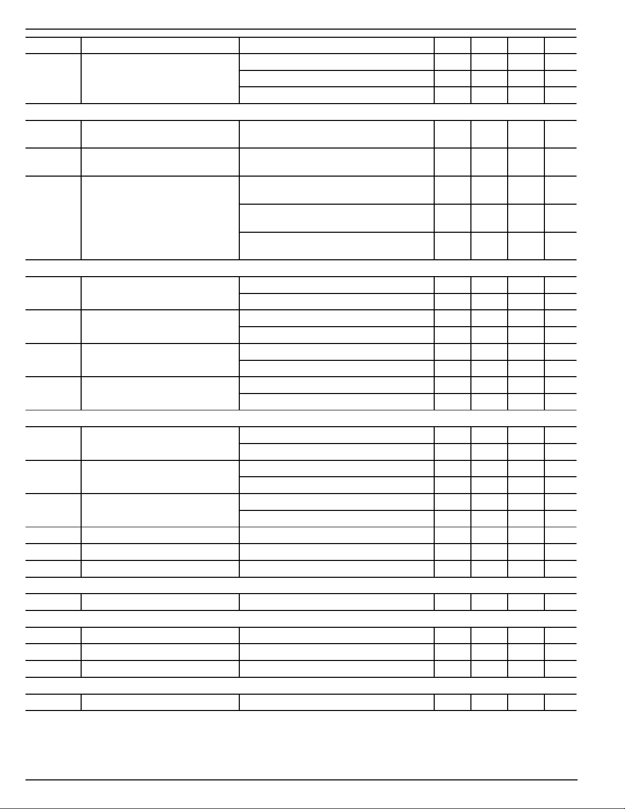
Symbol Parameter Conditions Min Typ Max Units
t
14
t
15
t
16
VCC Output
I
I
R
Hi-Z High Impedance Output shutdown mode, V
CC OUT
CCSC
O
VCC Switching Time (See Figure 3)
t
17
t
18
t
19
t
20
t
21
t
22
t
23
t
24
Power Supply
I
CC3
I
CC5
I
IN V
PP
V
CC3
V
CC5
V
PP
Thermal Shutdown
T
SD
Serial Interface DC Specifications
V
IH
V
IL
I
IN
Flag
I
FLG
Output Turnoff Delay Time, V
Notes 5, 7
OUT = 3.3V to Hi-Z, RL = 100Ω 150µs
PP
V
OUT = 5V to Hi-Z, RL = 100Ω 150µs
PP
V
OUT = 12V to Hi-Z, RL = 100Ω 150µs
PP
OUT = 0V 1 20 µA
CC
Leakage Current
Short Circuit Current Limit VCC OUT = 0, normal mode, 1.0 2.0 3.0 A
V
Switch Resistance V
Output Turn-On Delay Time, V
Note 5
Output Rise Time V
Output Fall Time V
Output Turnoff Delay, Notes 5, 6 V
V
IN Supply Current (3.3V) V
CC3
Note 7
V
IN Supply Current (5V) V
CC5
Note 8
IN Supply Current (12V) V
PP
Note 8
or V
CC3
OUT = 3.3V selected, 120 150 mΩ
CC
I
OUT = –1A (sourcing)
CC
OUT = 5V selected, 85 120 mΩ
V
CC
I
OUT = –1A (sourcing)
CC
OUT = 0V [ground] selected, 2000 3900 Ω
V
CC
I
OUT = 0.1mA (sinking)
CC
OUT = 0V to 10% of 3.3, RL = 10Ω 250 500 µs
CC
V
OUT = 0V to 10% of 5.0, RL = 10Ω 500 1000 µs
CC
OUT = 10% to 90% of 3.3V, RL = 10Ω 750 1200 5000 µs
CC
V
OUT = 10% to 90% of 5, RL = 10Ω 1000 2200 5000 µs
CC
OUT = 90% to 10% of 3.3, RL = 10Ω 100 550 1000 µs
CC
V
OUT = 90% to 10% of 5.0, RL = 10Ω 100 400 2000 µs
CC
OUT = 3.3V to 90% of 3.3V , RL = 10Ω 400 2000 µs
CC
V
OUT = 5V to 90% of 5V, RL = 10Ω 400 2000 µs
CC
OUT = 5V or 3.3V, I
CC
V
OUT = Hi-Z (sleep mode) 5 10 µA
CC
OUT = 5V or 3.3V, I
CC
V
OUT = Hi-Z (sleep mode) 0.2 10 µA
CC
OUT = 0V, 3.3V, 5V, or Hi-Z; I
PP
V
OUT = V
PP
switches, Note 4
CC5
OUT = 0 120 200 µA
CC
OUT = 0 25 50 µA
CC
OUT = 0 1 10 µA
PP
IN 4 50 µA
PP
Operating Input Voltage (3.3V) Note 7 3.0 3.3 5.5 V
Operating Input Voltage (5V) Note 8 — 5.0 5.5 V
Operating Input Voltage (12V) Note 8, 9 — 12 13.2 V
Thermal Shutdown Temperature 145 °C
Input Voltage: SDA, SCL, SLA pins
Input Voltage: SDA, SCL, SLA pins –0.3
0.7V
CC3
IN
5.5 V
0.3V
IN
CC3
V
Input Current 0V < VIN < 5.5V –1 0.2 1 µA
Flag Leakage Current V
= 5V 1 µA
FLG
MIC2564A 4 September 1999

MIC2564A Micrel
Symbol Parameter Conditions Min Typ Max Units
Serial Interface Timing Requirements (See Figure 1), Note 10
t
HD:DAT
t
SU:DAT
t
SU:SLA
t
SU:RST#
t
W
Note 1. Exceeding the absolute maximum rating may damage the device.
Note 2. The device is not guaranteed to function outside its operating rating.
Note 3. Devices are ESD sensitive. Handling precautions recommended.
Note 4. Output enabled into short circuit.
Note 5. Measurement is from the 50% point of the SLA rising edge.
Note 6. Measurement is from the Hi-Z- or 0V-state command to the beginning of the slope. Measurement does not apply when device is in current
Note 7. V
Note 8. V
Note 9. V
Note 10. Guaranteed by design not production tested.
SDA Hold Time 75 ns
SDA Setup Time data before clock 75 ns
Latch Setup Time 50 ns
Reset to Data Setup Time RST# before data 50 ns
Minimum Pulse Width clock (t
latch (t
reset (t
data (t
limit or thermal shutdown.
IN powers all internal logic, bias, and drive circuitry, and is required for operation.
CC3
and V
PP
IN must be either high impedance or greater than or approximately equal to the highest voltage V
PP
3.3V and 5V are connected to the MIC2564A, V
IN are not required for operation.
CC5
IN must be either 5V, 12V, or high impedance.
PP
)50ns
W:CLK
) 100 ns
W:SLA
)50ns
W:RST
)50ns
W:DA
in the system. For example, if both
CC
Serial Control Timing Diagram
t
W:DAT
RST#
t
SU:RST#
SDA
SLA
SCL
The MIC2564A uses a three-wire serial interface to control VCC and VPP outputs for both sections A and B. The three control
lines have thresholds compatible with both 3.3V and 5V logic families. Data (SDA) is clocked in on the rising clock edge. The
clock signal may be continuous or it may halt after all data is clocked in.
D8 D7 D6 D5 D4 D3 D2 D1 D0
t
SU:DAT
t
HD:DAT
t
W:CLK
t
Figure 1. Serial Control Timing Diagram
SU:SLA
t
W:SLA
September 1999 5 MIC2564A
 Loading...