

MICREL MIC2560-1BWM, MIC2560-0BWM Datasheet

MIC2560 Micrel
MIC2560
PCMCIA Card Socket VCC and VPP Switching Matrix
General Description
The MIC2560 VCC and VPP Matrix controls PCMCIA (Personal Computer Memory Card International Association)
memory card power supply pins, both VCC and VPP. The
MIC2560 switches voltages from the system power supply to
VCC and VPP. The MIC2560 switches between the three V
CC
voltages (OFF, 3.3V and 5.0V) and the VPP voltages (OFF,
0V, 3.3V, 5V, or 12.0V) required by PCMCIA cards. Output
voltage is selected by two digital inputs for each output and
output current ranges up to 1A for V
and 200mA for VPP.
CC
The MIC2560 provides power management capability under
the control of the PC Card controller and features overcurrent
and thermal protection of the power outputs, zero current
“sleep” mode, suspend mode, low power dynamic mode, and
on-off control of the PCMCIA socket power.
The MIC2560 is designed for efficient operation. In standby
(sleep) mode the device draws very little quiescent current,
typically 0.01µA. The device and PCMCIA ports are protected by current limiting and overtemperature shutdown.
Full cross-conduction lockout protects the system power
supply.
Ordering Information
Part Number Junction Temp. Range* Package
MIC2560-0BWM –40°C to +70°C 16-lead Wide SOP
MIC2560-1BWM –40°C to +70°C 16-lead Wide SOP
Refer to “Control Logic Table” for -0/-1 version explanation.
Applications
• PCMCIA power supply pin voltage switch
• Font cards for printers and scanners
• Data-collection systems
• Machine control data input systems
• Wireless communications
• Bar code data collection systems
• Instrumentation configuration/datalogging
• Docking stations (portable and desktop)
• Power supply sanagement
• Power analog switching
Features
• Complete PCMCIA VCC and VPP switch matrix
in a single IC
• No external components required
• Logic compatible with industry standard
PCMCIA controllers
• No voltage overshoot or switching transients
• Break-before-make switching
• Output current limit and overtemperature shutdown
• Digital flag for error condition indication
• Ultralow power consumption
• Digital selection of VCC and VPP voltages
• Over 1A VCC output current
• 200mA VPP (12V) output current
• Options for direct compatibility with
industry standard PCMCIA controllers
• 16-Pin SO package
Typical Application
System Power Supply
12V 3.3V 5V
Address and data lines
between logic controller and
PCMCIA cards not shown.
VPP IN
PCMCIA
Card Slot
Controller
Micrel, Inc. • 1849 Fortune Drive • San Jose, CA 95131 • USA • tel + 1 (408) 944-0800 • fax + 1 (408) 944-0970 • http://www.micrel.com
EN0
EN1
V
CC5
V
CC3
EN
EN
V
CC3
MIC2560
Power
Controller
GND
November 1999 1 MIC2560
IN
V
IN
CC5
VPP OUT
V
OUT
CC
V
V
Motherboard
1
PP
2
PP
V
CC
PCMCIA
Card
MIC2560 Micrel
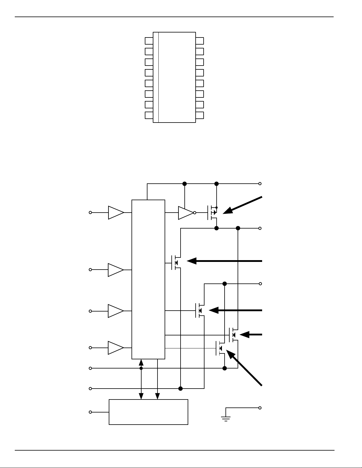
Pin Configuration
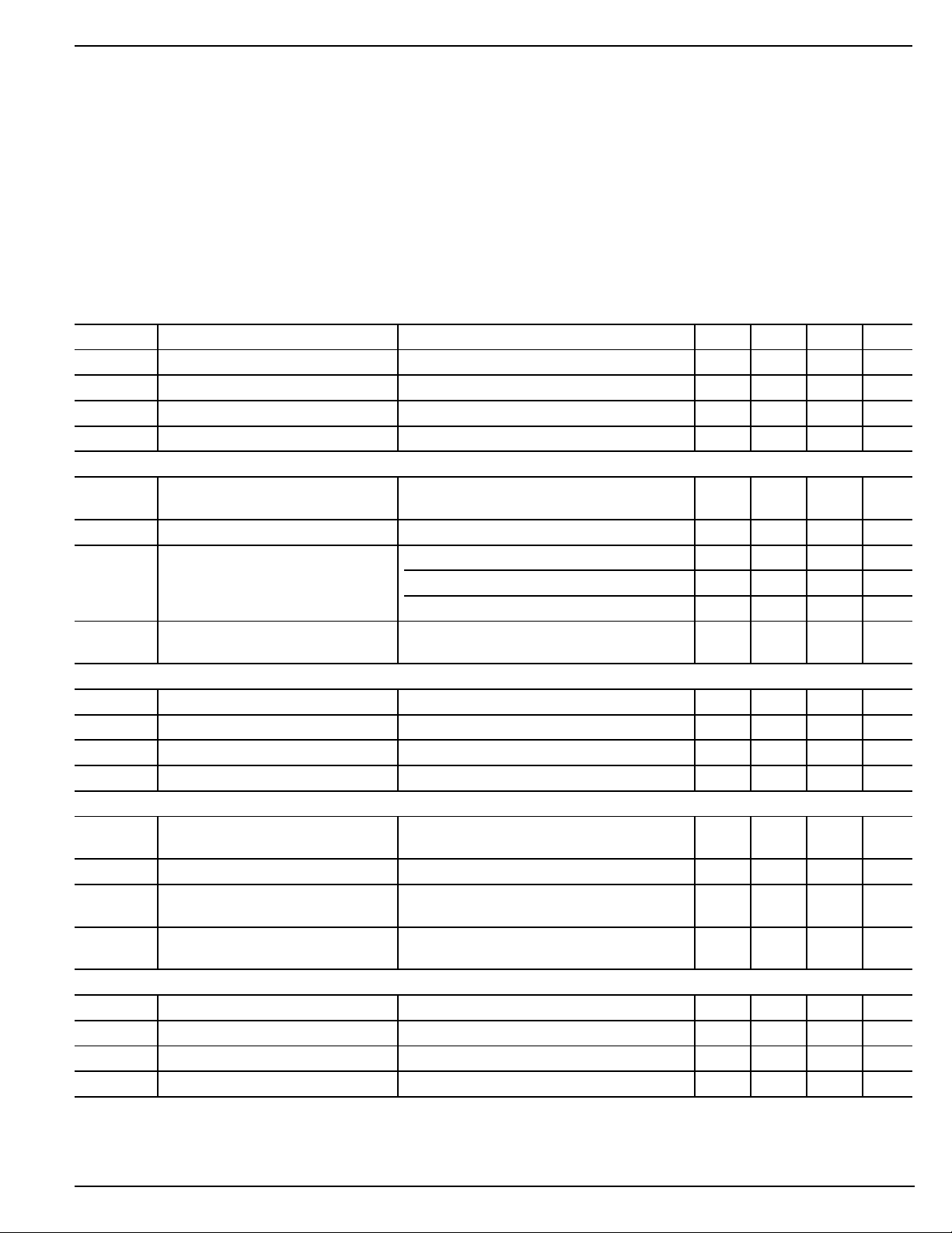
Logic Block Diagram
1V
IN
CC3
IN
GND
EN
EN
EN0
EN1
2
3
4
5
6
7
8
OUT
V
CC
V
CC3
V
CC5
V
CC3
16 V
15
14
13
12
11
10
9
OUT
CC
IN
V
CC5
VCC OUT
OUT
V
PP
IN
V
PP
NC
NC
FLAG
Both V
All three V
IN pins must be connected.
CC3
OUT pins must be connected.
CC
V
IN
PP
0.5Ω
V
CC5_EN
V
CC3_EN
V
CC3
EN1
EN0
IN
Control
Logic
V
PP OUT
0.7Ω
V
CC OUT
0.07Ω
2Ω
V
CC5
IN
Flag
I
/ Thermal Shut Down
Limit
0.04Ω
GND
MIC2560 2 November 1999
MIC2560 Micrel
Absolute Maximum Ratings (Notes 1 and 2)
Power Dissipation, T
AMBIENT
≤ 25°C ....
Internally Limited
SOP ............................................................. 800 mW
Derating Factors (To Ambient)
SOP ............................................................ 4 mW/°C
Storage Temperature ............................–65°C to +150°C
Maximum Operating Temperature (Die) ................ 125°C
Operating Temperature (Ambient) ..........–40°C to +70°C
Lead Temperature (5 sec)......................................260°C
Supply Voltage, V
V
IN ....................................................... V
CC3
V
IN ............................................................. 7.5V
CC5
...................................................
PP IN
Logic Input Voltages..................................–0.3V to +15V
Output Current (each Output)
V
PP OUT
V
CC OUT
V
CC OUT
............................
...................................
, Suspend Mode.............................. 600mA
>200mA, Internally Limited
>1A, Internally Limited
CC5
15V
IN
Electrical Characteristics:
(Over operating temperature range with V
Symbol Parameter Conditions Min Typ Max Units
Input
V
IH
V
IL
I
IN
Logic 1 Input Voltage 2.2 15 V
Logic 0 Input Voltage –0.3 0.8 V
Input Current 0 V < VIN < 5.5V ±1 µA
VPP Output
I
PP OUT
High-Impedance Output Shutdown Mode 1 10 µA
Hi-Z Leakage Current 1V ≤ V
I
PPSC
R
O
R
O
Short Circuit Current Limit V
Switch Resistance, select V
I
= –100mA (sourcing)
PP OUT
Switch Resistance, select V
I
= 50µA
PP OUT
VPP Switching Time
t
1
t
2
t
3
t
4
Output Turn-On Rise Time V
Output Turn-On Rise Time V
Output Turn-On Rise Time V
Output Rise Time V
VCC Output
I
CC OUT
High Impedance Output 1V ≤ V
Hi-Z Leakage Current, Note 3
I
CCSC
R
O
R
O
Short Circuit Current Limit V
Switch Resistance, I
V
CC OUT
= 5.0V
Switch Resistance, I
V
CC OUT
= 3.3V
VCC Switching Time
t
1
t
2
t
3
t
4
Rise Time V
Rise Time V
Fall Time V
Rise Time V
IN = 3.3V, V
CC3
IN = 5.0V, VPP IN = 12V unless otherwise specified.)
CC5
OUT ≤ 12V
PP
= 0 0.2 A
PP OUT
OUT = 12V 0.55 1 Ω
PP
select V
select V
PP
PP
PP
PP
CC OUT
CC OUT
CC OUT
CC OUT
CC OUT
CC OUT
CC OUT
OUT = 5V 0.7 1 Ω
PP
OUT = 3.3V 2 3 Ω
PP
= clamped to ground 0.75 2 kΩ
PP OUT
OUT = hi-Z to 5V 50 µs
OUT = hi-Z to 3.3V 40 µs
OUT = hi-Z to 12V 300 µs
OUT = 3.3V or 5V to 12V 300 µs
≤ 5V 1 10 µA
CC OUT
= 0 1 2 A
= –1000mA (sourcing) 70 100 mΩ
= –1000mA (sourcing) 40 66 mΩ
= 0V to 3.3V, I
= 0V to 5.0V, I
= 1A 100 600 µs
OUT
= 1A 100 500 µs
OUT
= 5.0V to 3.3V 300 µs
= hi-Z to 5V 400 µs
November 1999 3 MIC2560
MIC2560 Micrel
Symbol Parameter Conditions Min Typ Max Units
Power Supply
I
CC5
I
CC3
I
IN V
PP
V
IN Operating Input Voltage V
CC5
V
IN Operating Input Voltage V
CC3
V
PP IN
Suspend Mode (Note 4)
I
CC3
R
ON VCC
Note 1. Functional operation above the absolute maximum stress ratings is not implied.
Note 2. Static-sensitive device. Store only in conductive containers. Handling personnel and equipment should be grounded to prevent damage from
Note 3. Leakage current after 1,000 hours at 125°C may increase up to five times the initial limit.
Note 4. Suspend mode is a pseudo-power-down mode the MIC2560 automatically allows when V
V
IN Supply Current I
CC5
V
IN Supply Current V
CC3
IN Supply Current VCC active, V
PP
(I
PP OUT
= 0)
= 0 0.01 10 µA
CC OUT
CC OUT
V
CC OUT
V
PP OUT
CC5
CC3
= 5V or 3.3V, I
= hi-Z (Sleep mode) 0.01 10 µA
= 5V or 3.3V 15 50 µA
PP OUT
= hi-Z, 0 or V
IN ≥ V
CC3
IN ≤ V
CC5
PP
IN V
IN 2.8 3.3 V
= 0 30 50 µA
CC OUT
0.01 10 µA
IN 5.0 6 V
CC3
CC5
IN V
Operating Input Voltage 8.0 12.0 14.5 V
Active Mode Current V
V
CC OUT RON
= 0V, V
PP IN
= enabled
V
CC3
VPP = disabled (hi-Z or 0V)
V
= 0V, V
PP IN
V
= enabled
CC3
CC5
CC5
= V
= V
CC3
CC3
= 3.3V 30 µA
= 3.3V 4.5 Ω
VPP = disabled (hi-Z or 0V)
static discharge.
= 0V, VPP OUT is deselected, and VCC OUT =
3.3V is selected. Under these conditions, the MIC2560 functions in a reduced capacity mode where VCC output of 3.3V is allowed, but at
lower current levels (higher switch on-resistance).
PP IN
MIC2560 4 November 1999
 Loading...