

MICREL MIC2558BM Datasheet
MIC2558 Micrel
MIC2558
PCMCIA Dual Card Socket VPP Switching Matrix
General Description
The MIC2558 Dual VPP Matrix switches the four voltages
required by PCMCIA (Personal Computer Memory Card
International Association) card V
PP1
and V
Pins. The
PP2
MIC2558 provides selectable 0V, 3.3V, 5.0V, or 12.0V (±5%)
from the system power supply to V
PP1
and V
. Output
PP2
voltage is selected by two digital inputs per VPP pin. Output
current ranges up to 120mA. Four output states, VPP, VCC,
high impedance, and active logic low are available, and V
is independent of V
. An auxiliary control input determines
PP2
PP1
whether the high impedance (open) state or low logic state is
asserted.
In standby mode or full operation, the device draws very little
quiescent current, typically less than 1µA.
The MIC2558 is available in a 14-pin SOIC and a 14-pin
plastic DIP.
Applications
• PCMCIA VPP Pin Voltage Switch
• Power Supply Management
Features
• Complete PCMCIA VPP Switch Matrix in a Single IC
• Dual Matrix allows independent V
PP1
and V
PP2
• Digital Selection of 0V, VCC, VPP, or High
Impedance Output
• No V
PPOUT
Overshoot or Switching Transients
• Break-Before-Make Switching
• Ultra Low Power Consumption
• 120mA VPP (12V) Output Current
• Optional Active Source Clamp for Zero Volt Condition
• 3.3V or 5V Supply Operation
• 14-Pin SOIC Package
Ordering Information
Part Number Temperature Range Package
MIC2558BM –40°C to +85°C 14-pin SOIC
MIC2558BM T&R –40°C to +85°C 14-SO Tape & Reel*
* 2,500 Parts per reel.
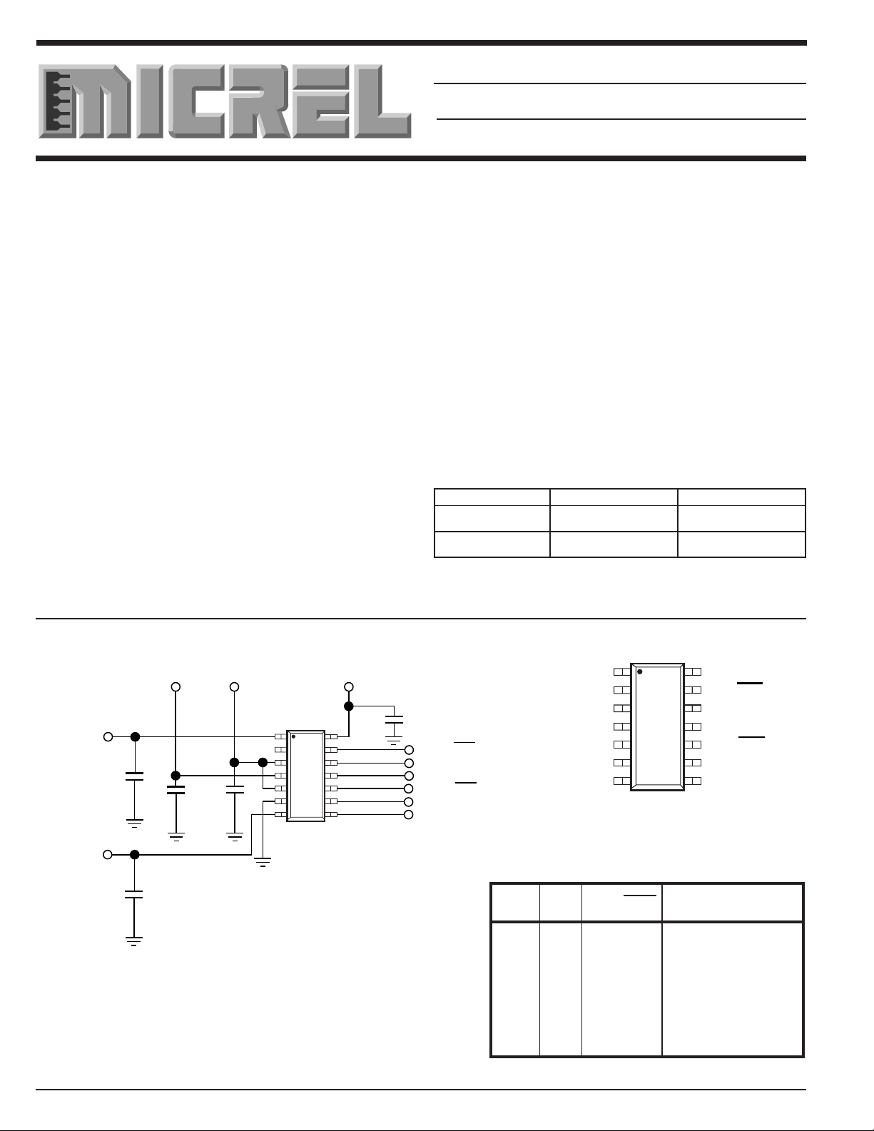
Typical Application
V
PP IN
+12V
V
PP OUT 1
V
PP OUT 2
0.1µF
0.1µF
1µF 1µF
V
CC
+3.3V or +5V
2
3
MIC2558
4
5
6
7
Pin Configuration
V
DD
+5V
0.1µF
14
13
12
11
10
9
8
Hi-Z/ Low 1 Control
EN0
1
EN1
1
Hi-Z/ Low 2 Control
EN0
2
EN1
2
V
V
PP
PP
OUT1
+V
CC1
V
PP
+V
CC2
GND
OUT2
NC
IN
2
3
MIC2558
4
5
6
7
EN1 EN0 Hi-Z/Low V
0 0 0 0V, (Sink current)
0 0 1 Hi-Z (No Connect)
01 x VCC (3.3V or 5.0V)
10 x V
1 1 x Hi-Z (No Connect)
14
13
12
11
10
9
8
PP OUT
PP
V
DD
Hi-Z/Low1
EN0
1
EN1
1
Hi-Z/Low2
EN0
2
EN1
2
2-10 1997
MIC2558 Micrel
Absolute Maximum Ratings (Notes 1 and 2)
Power Dissipation, T
SOIC 800 mW
Derating Factors (To Ambient)
SOIC 4 mW/°C
Storage Temperature –65°C to +150°C
Operating Temperature (Die) 125°C
Operating Temperature (Ambient) –40°C to +85°C
Lead Temperature (5 sec) 260°C
AMBIENT
≤ 25°C
Supply Voltage, V
V
CC
V
DD
Logic Input Voltages –0.3V toV
Output Current (each Output)
V
PP OUT
V
PP OUT
PP IN
= 12V 600mA
= V
CC
15V
7.5V
7.5V
DD
250mA
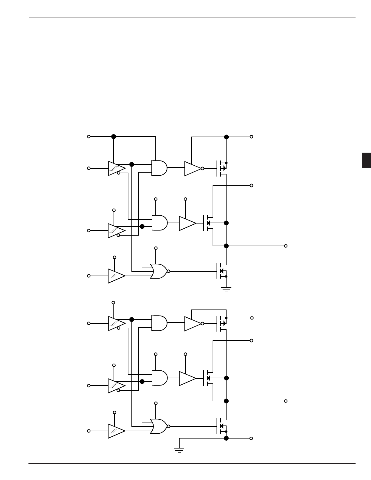
Logic Block Diagram
V
DD
EN1
EN0
HiZ/
LOW
V
14
PP IN
4
2
1
11
V
CC1
V
DD
V
DD
1
12
V
DD
13
1
V
DD
V
DD
V
PP IN
3
V
PP OUT1
1
EN1
2
8
V
PP IN
EN0
V
DD
V
DD
2
9
V
DD
V
DD
HiZ/
LOW
1997 2-11
10
2
5
6
V
PP IN
V
CC2
GND
7
V
PP OUT2
 Loading...