

MICREL MIC2550BTS Datasheet
MIC2550 Micrel
MIC2550
Universal Serial Bus Transceiver
Advance Information
General Description
The MIC2550 is a single-chip transceiver that complies with
the physical layer specifications for Universal Serial Bus
(USB).
The MIC2550 supports full-speed (12Mb/s) dual supply voltage operation (patent pending) and low-speed (1.5Mb/s)
operation.
A unique dual supply voltage operation allows the MIC2550
to reference the system I/F I/O signals to a supply voltage
down to 2.5V while independently powered by the USB V
This allows the system interface to operate at its core voltage
without addition of buffering logic and also reduce system
operating current.
BUS
Features
• Compliant to
• Operation down to 2.5V
• Dual supply voltage operation
• Supports full-speed (12Mb/s) and
low-speed (1.5Mb/s) operation
• Speed-select termination supply
• Very low power consumption meets
USB suspend-current requirements
• Small 14-pin TSSOP
.
USB Specification Revision 1.1
Applications
• Personal digital assistants (PDA)
• Palmtop computers
• Cellular telephones
Ordering Information
Part Number Junction Temp. Range Package
MIC2550BTS –40°C to +85°C 14-Pin TSSOP
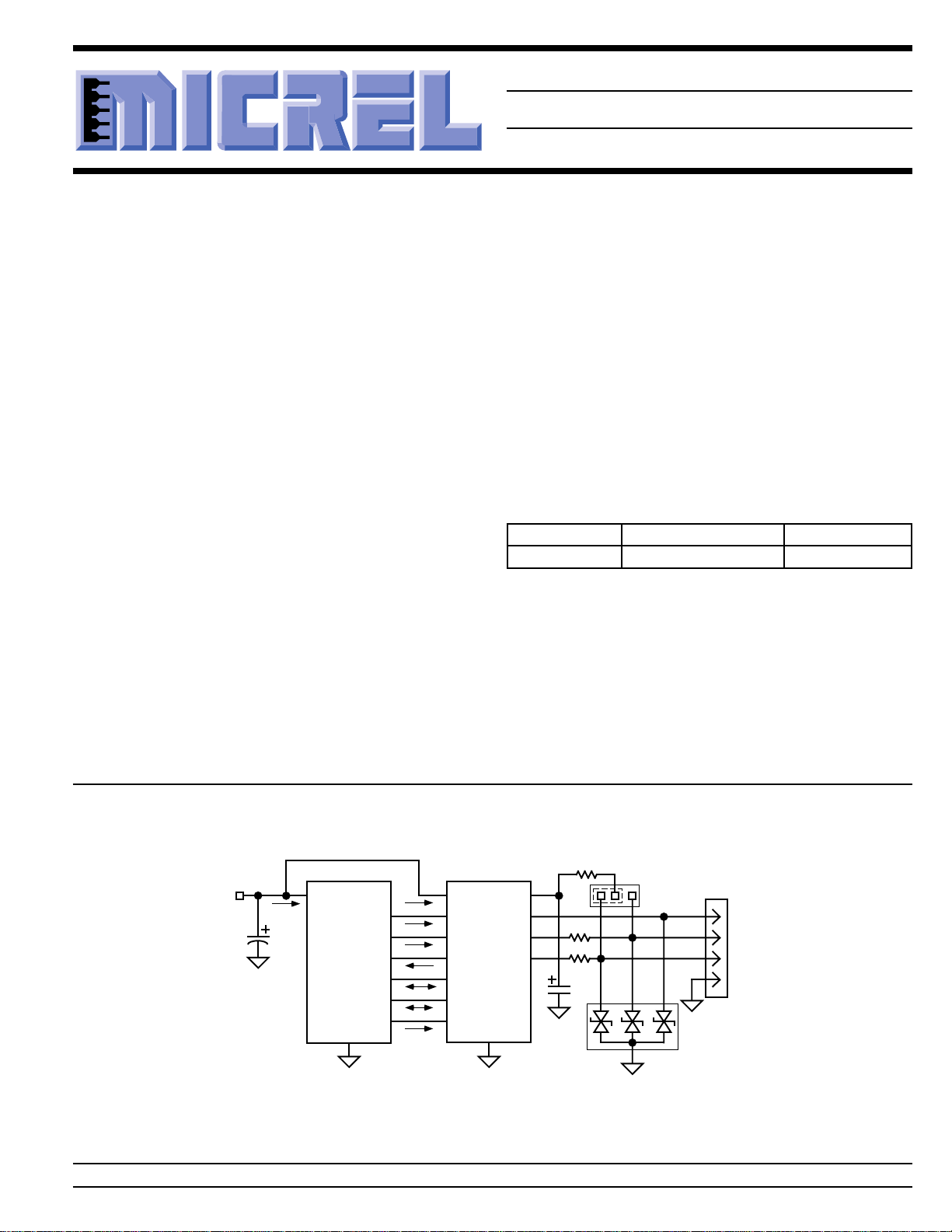
System Diagram
System
Supply
Voltage
0.47µF
Micrel, Inc. • 1849 Fortune Drive • San Jose, CA 95131 • USA • tel + 1 (408) 944-0800 • fax + 1 (408) 944-0970 • http://www.micrel.com
System
Interface
GND
MIC2550
VIF
SPD
OE#
RCV
VP
VM
SUS
GND
VTRM
VBUS
D+
D–
October 4, 1999 1 MIC2550
1.5k
LOW
SPEED
24Ω
24Ω
1µF
HIGH
SPEED
V
BUS
D+
D–
GND
USB
Interface
Connector
MIC2550 Micrel
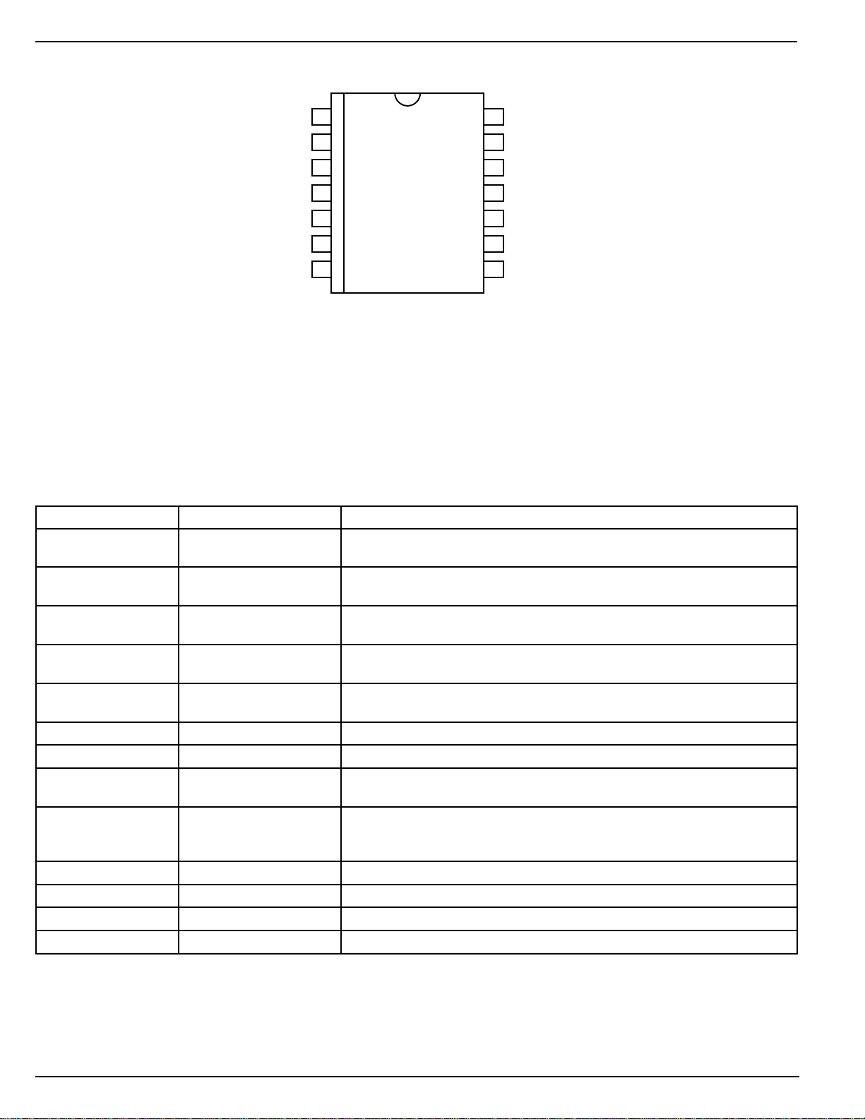
Pin Configuration
1VIF VBUS
2
SPD
RCV
3
4VP
5
VM
6NC
GND
7
Pin Description
Pin Number Pin Name Pin Function
1 VIF System Interface Supply Voltage (Input): Determines logic voltage levels for
2 SPD Speed (Input): Edge rate control. Logic high selects full-speed edge rates.
3 RCV Receive Data (Output): System interface receive data interface to logic
4 VP Plus (Input/Output): System interface signal to logic controller. If OE# is
5 VM Minus (Input/Output): System interface signal to logic controller. If OE# is
6, 13 NC not internally connected
7 GND Ground: Power supply return and signal reference.
8 SUS Suspend (Input): Logic high turns off internal circuits to reduce supply
9 OE# Output Enable (Input): Active-low system interface input signal from from
10 D– USB Differential Data Line – (Input/Output)
11 D+ USB Differential Data Line + (Input/Output)
12 VTRM Termination Supply (Output): 3.3V speed termination resistor supply output.
14 VBUS USB Supply Voltage (Input): Transceiver supply.
14
13
NC
12
VTRM
11
D+
10
D–
9
OE#
8
SUS
14-Pin TSSOP (TM)
system interface signaling to logic controller.
Logic low selects low-speed edge rates.
controller.
logic 1, VP is a receiver output (+); If OE# is logic 0, VP is a driver input (+).
logic 1, VM is a receiver output (–); If OE# is logic 0, VM is a driver input (–).
current.
logic controller. Logic low causes transceiver to transmit data onto the bus.
Logic high causes the transceiver to receive data from the bus.
MIC2550 2 October 4, 1999
MIC2550 Micrel
Absolute Maximum Ratings (Note 1)
Supply Voltage (VIF)...................................................+6.5V
Input Voltage (V
Output Current (ID+, ID–)...........................................±50mA
Output Current (all others) .......................................±15mA
Input Current ............................................................±50mA
) ........................–0.5V(min)/5.5V(max)
BUS
Operating Ratings (Note 2)
Supply Voltage (V
Temperature Range (TA) ........................... –40°C to +85°C
Junction Temperature (TJ) ........................................ 160°C
Package Thermal Resistance
TSSOP (θJA) .....................................................100°C/W
) ................................. 4.0V to 5.25V
BUS
Power Dissipation (PD) ................................................TBD
Storage Temperature (TS) ..........................–65° to +150°C
ESD, Note 3
Electrical Characteristics
TA = 25°C, bold values indicate –40°C ≤ TA ≤ +85°C; typical values at V
V
= 4.0V to 5.25V, VIF = 2.5V to 3.6V; unless noted.
BUS
Symbol Parameter Condition Min Typ Max Units
System and USB Interface DC Characteristics
V
V
V
V
V
V
I
I
BUS
IF
IL
IH
OH
OL
IL
IF
USB Supply Voltage 4.0 5.25 V
System I/F Supply voltage 2.5 5.25 V
Low-Level Input Voltage, Note 4 0.15V
High-Level Input Voltage, Note 4 0.85V
High-Level Output Voltage, Note 4 IOH = 20µA 0.9V
Low-Level Output Voltage, Note 4 IOL = 20µA 0.1 V
Input Leakage Current, Note 4 ±5 µA
System I/F Supply Current D– and D+ are idle, VIF = 3.6V, V
SUS = 1, OE# = 1
D– and D+ are idle, V
SUS = 0, OE# = 1
D– and D+ active, C
SUS = 0, VIF = 3.6V, OE# = 0
D– and D+ active, C
SUS = 0, VIF = 3.6V, OE# = 0
I
BUS
USB Supply Current D– and D+ are idle, V
SUS = 1, OE# = 1
D– and D+ are idle, V
SUS = 1, OE# = 1
D– and D+ are idle, V
SUS = 0, OE# = 0
D– and D+ are idle, V
SUS = 0, OE# = 1
D– and D+ active, C
SUS = 0, V
BUS
D– and D+ active, C
V
TRM
Termination Voltage I
SUS = 0, V
TRM
BUS
= 2.5mA 3.0 3.6 V
= 5.0V, VIF = 3.0V; minimum and maximum values at
BUS
IF
IF
= 5.25V 1 µA
BUS
LOAD
LOAD
LOAD
= 5.25V
LOAD
= 5.25V
= 3.6V, V
IF
= 50pF, SPD = 1, 2 µA
= 600pF, SPD = 0, 2 µA
= 5.25V, SPD = 0 140 200 µA
BUS
= 5.25V, SPD = 1 140 200 µA
BUS
= 5.25V, SPD = 0 140 200 µA
BUS
= 5.25V, SPD = 1 200 350 µA
BUS
= 50pF, SPD = 1, mA
= 600pF, SPD = 0 mA
= 5.25V 1 µA
BUS
V
IF
V
V
October 4, 1999 3 MIC2550
 Loading...