

MICREL MIC2537-1BM, MIC2537-2BM Datasheet
MIC2537 Micrel
MIC2537
Quad Power Distribution Switch
Preliminary Information
General Description
The MIC2537 is a cost-effective high-side power switch with
four independently controlled channels, optimized for buspowered Universal Serial Bus (USB) applications. Few external components are necessary to satisfy USB requirements.
The MIC2537 satisfies the following USB requirements: each
switch channel supplies up to 100mA as required by USB
bus-powered downstream devices; fault current is limited to
typically 250mA, well below the UL 25VA safety requirements; and a flag output is available to indicate fault conditions to the local USB controller. Soft start eliminates the
momentary voltage drop on the upstream port that may occur
when the switch is enabled in bus-powered applications.
Additional features include thermal shutdown to prevent
catastrophic switch failure from high-current loads and 3.3V
and 5V logic compatible enable inputs.
The MIC2537 is available in active-high and active-low versions in a 16-lead SOP package.
Features
• Compliant to USB specifications
• 3V to 5.5V input
• 100mA minimum continuous load current per port
• 425mΩ typical on-resistance
• < 400mA current limit
• Individual open-drain fault flag leads
• 3V/5V-compatible enable inputs
• Active-high (-1) and active-low (-2) versions
• 100µA max. on-state supply current
• <1µA typical off-state supply current
• 16-lead SOP package
•–40°C to 85°C operation
Applications
• USB keyboards
• USB bus-powered docking stations
• Notebook docking stations
• Notebook PCs
• PDA
• General power distribution
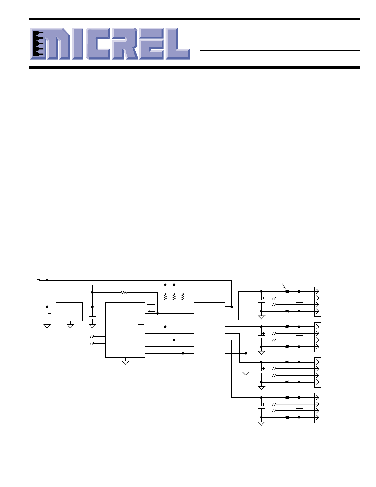
Typical Application
Upstream V
4.75V to 5.25V
500mA max.
4.7
µF
BUS
MIC5207-3.3
LDO Regulator
IN OUT
GND
Bold lines indicate
0.1" wide, 1-oz. copper
high-current traces.
* 33µF, 16V tantalum or 100µF, 10V electrolytic per port
1µF
10k
3.3V USB Controller
GND
EN
OC
EN
OC
EN
OC
EN
OC
V+
D+
D–
10k 10k 10k
MIC2537
ENA
FLGA NC
ENB OUTA
FLGB
OUTB
ENC
OUTC
OUTDFLGC
END
FLGD
NC
GND
Ferrite
Bead
V
BUS
33µF*
IN
0.1
µF
33µF*
33µF*
33µF*
0.01µF
0.01µF
0.01µF
0.01µF
D+
D–
GND
V
BUS
D+
D–
GND
V
BUS
D+
D–
GND
V
BUS
D+
D–
GND
Downstream
USB
Port 1
100mA max.
Downstream
USB
Port 2
100mA max.
Downstream
USB
Port 3
100mA max.
Downstream
USB
Port 4
100mA max.
Typical Bus-Powered Hub
Micrel, Inc. • 1849 Fortune Drive • San Jose, CA 95131 • USA • tel + 1 (408) 944-0800 • fax + 1 (408) 944-0970 • http://www.micrel.com
December 1999 1 MIC2537
MIC2537 Micrel
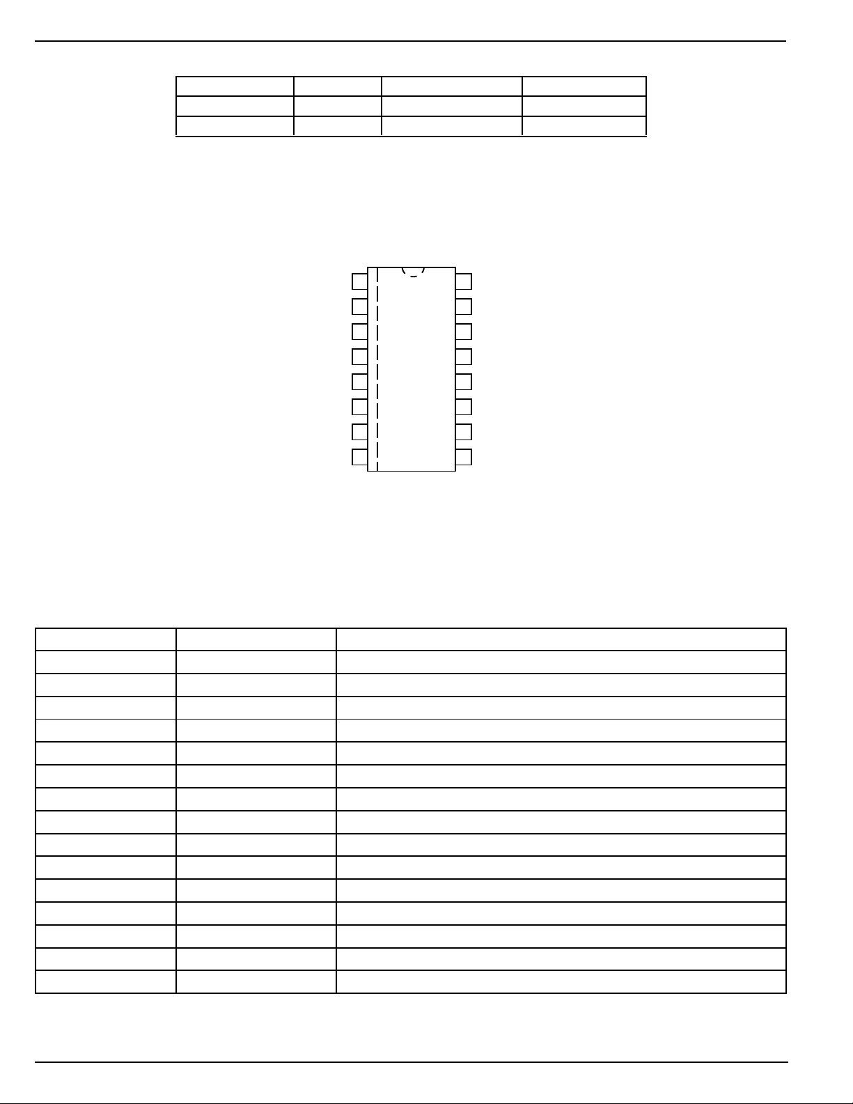
Ordering Information
Part Number Enable Temperature Range Package
MIC2537-1BM Active High –40°C to +85°C 16-Lead SOP
MIC2537-2BM Active Low –40°C to +85°C 16-Lead SOP
Pin Configuration
MIC2537-x
FLGA
ENA
1
2
16
15
FLGD
END
OUTA
GND
NC
OUTB
ENB
FLGB
Pin Description
Pin Number Pin Name Pin Function
1 FLGA Flag A: (Output): Channel A open-drain fault flag output.
2 ENA Enable A (Input): Channel A control input.
3 OUTA Output A: Channel A switch output.
4 GND Ground: Supply return. Connect both leads to ground.
5, 12 NC Not internally connected
6 OUTB Output B: Channel B switch output.
7 ENB Enable B (Input): Channel B control input.
8 FLGB Flag B (Output): Channel B open-drain fault flag output.
9 FLGC Flag C (Output): Channel C open-drain fault flag output.
10 ENC Enable C (Input): Channel C control input.
11 OUTC Output C: Channel C switch output.
13 IN Positive Supply Input
14 OUTD Output D: Channel D switch output.
15 END Enable D (Input): Channel D control input.
16 FLGD Flag D (Output): Channel D open-drain fault flag output.
3
4
5
6
7
8
16-Lead SOP (M)
14
13
12
11
10
9
OUTD
IN
NC
OUTC
ENC
FLGC
December 1999 2 MIC2537

MIC2537 Micrel
Absolute Maximum Ratings (Note 1)
Supply Voltage (V
Fault Flag Voltage (V
Fault Flag Current (I
Output Voltage (V
Output Current (I
Control Input (V
) .....................................................+6V
IN
)..............................................+6V
FLG
) ............................................25mA
FLG
) ..................................................+6V
OUT
)...............................Internally Limited
OUT
)......................................... –0.3V to 12V
EN
Operating Ratings (Note 2)
Supply Voltage (V
Ambient Operating Temperature (T
Thermal Resistance
SOP (θ
) ..........................................................120°C/W
JA
) ...................................... +3V to +5.5V
IN
) ........ –40°C to +85°C
A
Storage Temperature (TS) ....................... –65°C to +150°C
Lead Temperature (Soldering 5 sec.) ....................... 260°C
ESD Rating, Note 3....................................................... 2kV
Electrical Characteristics
VIN = +5V; TA = 25°C; unless noted.
Parameter Condition Min Typ Max Units
Supply Current Note 4, switch off, OUTA–D = open 0.75 5 µA
Note 4, all switches on, OUTA–D = open 70 100 µA
Enable Input Threshold low-to-high transition 1.8 2.4 V
high-to-low transition, Note 4 0.8 1.6 V
Enable Input Current VEN = V
VEN = V
Enable Input Capacitance 1pF
Switch Resistance single switch, 100mA load 425 700 mΩ
Output Turn-On Delay RL = 50Ω, CL = 1µF, Note 5 0.51 ms
Output Turn-On Rise Time RL = 50Ω, CL = 1µF, Note 5 0.2 0.5 ms
Output Turnoff Delay RL = 50Ω, CL = 1µF, Note 5 150 300 µs
Output Turnoff Fall Time RL = 50Ω, CL = 1µF, Note 5 148 300 µs
Output Leakage Current each output (switch off) 1 10 µA
Current Limit Threshold ramped load applied to enable output, Note 6 300 500 mA
Continuous Load Current each output, FLG not active 100 mA
Short Circuit Current Limit each output (enabled into load), V
Overtemperature Shutdown TJ increasing 135 °C
Threshold TJ decreasing 125 °C
Error Flag Output Resistance VIN = 5V, IL = 10mA 10 Ω
VIN = 3.3V, IL = 10mA 12 Ω
Error Flag Off Current V
Note 1. Exceeding the absolute maximum rating may damage the device.
Note 2. The device is not guaranteed to function outside its operating rating.
Note 3. Devices are ESD sensitive. Handling precautions recommended. Human body model, 1.5kΩ in series with 100pF.
Note 4. Off is ≤ 0.8V and on is ≥ 2.4V for the MIC2537-1. Off is ≥ 2.4V and on is ≤ 0.8V for the MIC2537-2. The enable input has approximately
200mV of hysteresis. See control threshold charts.
Note 5. See “Timing Diagrams.”
Note 6. See “Functional Characteristics: Current-Limit Response” graph.
= 5V 0.01 1 µA
FLAG
= 2.4V 0.01 1 µA
OH(min)
= 0.8V 0.01 1 µA
OL(max)
= 4.0V 150 250 400 mA
OUT
December 1999 3 MIC2537
MIC2537 Micrel
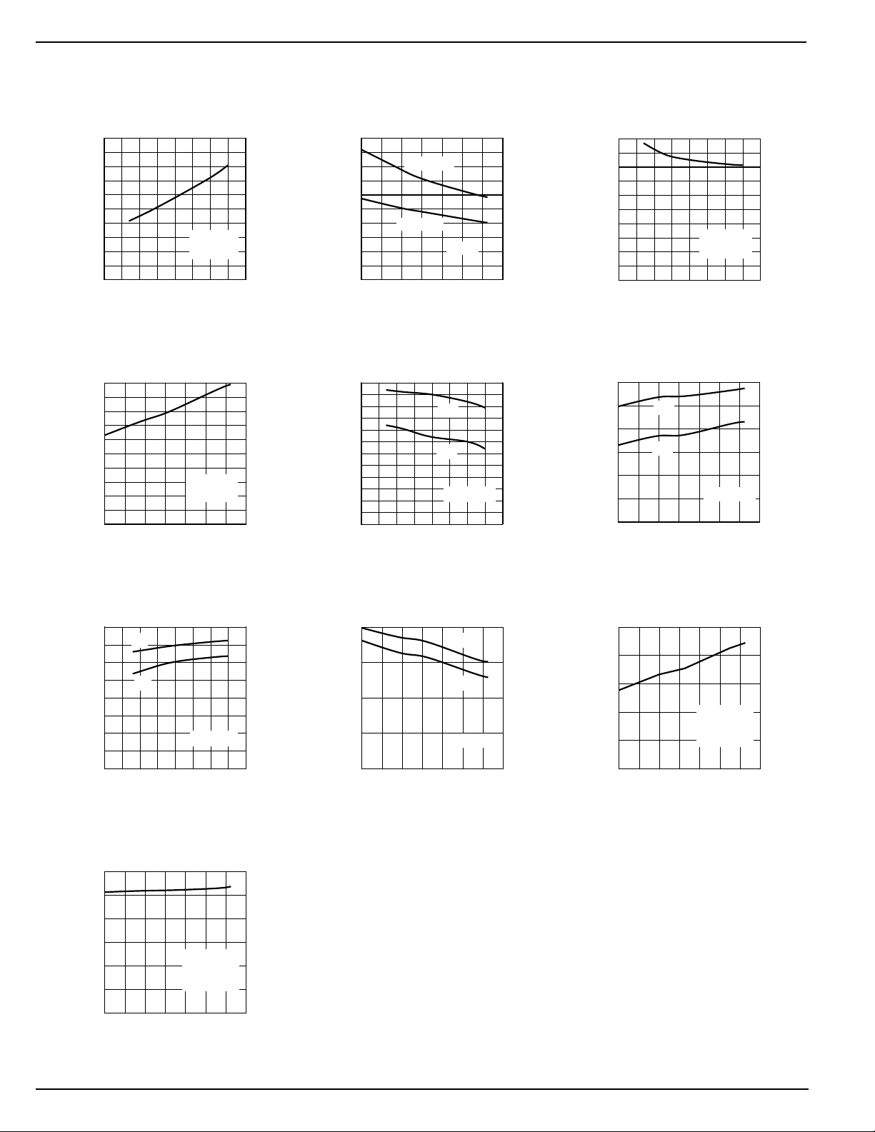
Typical Characteristics
Supply Current
vs. Supply Voltage
100
80
60
40
20
SUPPLY CURRENT (µA)
0
23456
SUPPLY VOLTAGE (V)
TA = 25°C
R
= ∞
L
Ouput On-Resistance
Variation vs. Temperature
500
400
300
200
100
ON RESISTANCE (mΩ)
0
-40 -20 0 20 40 60 80 100
TEMPERATURE (°C)
VIN = 5V
I
= 100mA
L
Supply Current
100
SUPPLY CURRENT (µA)
vs. Temperature
80
60
40
20
0
-40 -20 0 20 40 60 80 100
VIN = 5V
VIN = 3.3V
RL = ∞
TEMPERATURE (°C)
Overcurrent Threshold and
Current Limit vs. Supply Voltage
300
250
200
150
100
CURRENT (mA)
50
0
23456
SUPPLY VOLTAGE (V)
I
THR
I
LIM
TA = 25°C
Ouput On-Resistance
Variation vs. Supply Voltage
500
400
300
200
100
ON-RESISTANCE (mΩ)
0
23456
SUPPLY VOLTAGE (V)
TA = 25°C
I
= 100mA
L
Overcurrent Threshold, and
Current Limit vs. Temperature
300
250
200
150
100
CURRENT (mA)
50
0
-40 -20 0 20 40 60 80 100
I
THR
I
LIM
VIN = 5V
TEMPERATURE (°C)
Control Threshold
vs. Supply Voltage
2.0
1.5
1.0
0.5
ENABLE VOLTAGE (V)
V
IH
V
IL
TA = 25°C
0
23456
SUPPLY VOLTAGE (V)
Output Fall Time
1.5
1.0
TIME (µs)
0.5
vs. Temperature
VIN = 5V
C
= 0.01µF
L
R
= 44Ω
L
0
-40 -20 0 20 40 60 80 100
TEMPERATURE (°C)
Control Threshold
vs. Temperature
2.0
1.5
1.0
0.5
THRESHOLD VOLTAGE (V)
0
-40 -20 0 20 40 60 80 100
TEMPERATURE (°C)
V
IH
V
IL
VIN = 5V
Output Rise Time
vs. Temperature
VIN = 5V
C
= 0.01µF
L
R
= 44Ω
L
0
-40 -20 0 20 40 60 80 100
TEMPERATURE (°C)
TIME (µs)
500
400
300
200
100
December 1999 4 MIC2537
 Loading...