

MICREL MIC2525-2BN, MIC2525-2BM, MIC2525-1BM, MIC2525-1BN Datasheet
MIC2525 Micrel
MIC2525
USB Power Control Switch
Not Recommended for New Designs
Refer to MIC2025
General Description
The MIC2525 is an integrated high-side power switch, optimized for self-powered and bus-powered Universal Serial
Bus (USB) applications. Few external components are necessary to satisfy USB requirements.
The MIC2525 satisfies the following USB requirements: each
switch channel supplies up to 500mA as required by USB
downstream devices; the switch’s low on-resistance meets
USB voltage drop requirements; fault current is limited to
typically 750mA, well below the UL 25VA safety requirements; and a flag output is available to indicate fault conditions to the local USB controller. Soft start eliminates the
momentary voltage drop on the upstream port that may occur
when the switch is enabled in bus-powered applications.
Additional features include thermal shutdown to prevent
catastrophic switch failure from high-current loads,
undervoltage lockout (UVLO) to ensure that the device remains off unless there is a valid input voltage present, and
3.3V and 5V logic compatible enable inputs.
The MIC2525 is a UL recognized component and is available
in active-high and active-low versions in 8-pin DIP and SOIC
packages.
For new designs, please see the MIC2025/2075.
Features
• Compliant to USB specifications
• UL Recognized Component
• 3V to 5.5V input
• 500mA minimum continuous load current per port
• 140mΩ maximum on-resistance
• 1.25A maximum short circuit current limit
• Open-drain fault flag pins
• 110µA typical on-state supply current
• 1µA typical off-state supply current
• Output can be forced higher than input (off-state)
• Thermal shutdown
• 2.4V typical undervoltage lockout (UVLO)
• 1ms turn-on (soft-start) and fast turnoff
• Active-high or active-low enable versions
• 8-pin SOIC and DIP packages
Applications
• USB hosts and self-powered hubs
• USB bus-powered hubs
• Hot plug-in power supplies
• Battery-charger circuits
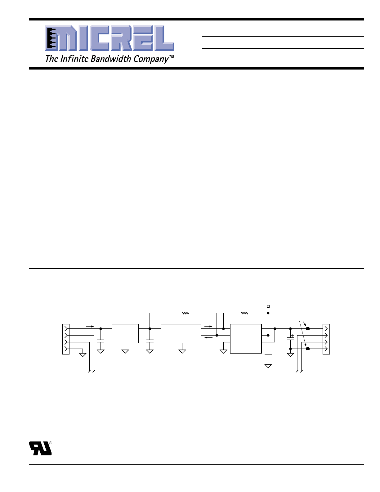
Typical Application
4.50V to 5.25V
Upstream V
100mA max.
BUS
V
BUS
D+
D–
GND
Data
1µF
MIC5207-3.3
IN OUT
GND
3.3V
VIN
1µF
10k
ON/OFF
OVERCURRENT
GND
100k
MIC2525-23.3V USB Controller
EN OUT
FLG IN
GND OUT
NC
Single-Port USB Self-Powered Hub
NC
V
CC
5.0V
0.1µF
150µF
Ferrite
Beads
Data
V
BUS
D+
D–
GND
USB
Port
UL Recognized Component
Micrel, Inc. • 1849 Fortune Drive • San Jose, CA 95131 • USA • tel + 1 (408) 944-0800 • fax + 1 (408) 944-0970 • http://www.micrel.com
January 2000 1 MIC2525
MIC2525 Micrel
Ordering Information
Part Number Enable Temperature Range Package
MIC2525-1BM Active High –40°C to +85°C 8-Pin SOIC
MIC2525-2BM Active Low –40°C to +85°C 8-Pin SOIC
MIC2525-1BN Active High –40°C to +85°C 8-pin DIP
MIC2525-2BN Active Low –40°C to +85°C 8-pin DIP
Pin Configuration
MIC2525
EN
1
OUT
8
FLG
GND
NC
(EN) 1
(FLG) 2
Pin Description
Pin Number Pin Name Pin Function
1 EN Enable (Input): Logic-compatible enable input. High input > 2.1V typical.
2 FLG Fault Flag (Output): Active-low, open-drain output. Indicates overcurrent,
3 GND Ground: Supply return.
4, 5 NC Not internally connected. (For pin compatibility with the MIC2505, connect
7 IN Supply Input: Output MOSFET drain. Also supplies IC’s internal circuitry.
6, 8 OUT Switch Output: Output MOSFET source. Typically connect to switched side
2
3
4
IN
7
OUT
6
NC
5
8-Pin SOIC (M)
8-Pin DIP (N)
MIC2525
LOGIC,
CHARGE
PUMP
3 (GND)
Low input <1.9V typical (-1 active high, -2 active low).
UVLO and thermal shutdown.
pin 7 to pin 5 and leave pin 4 unconnected.)
Connect to positive supply.
of load.
6, 8 (OUT)
7 (IN)
MIC2525 2 January 2000

MIC2525 Micrel
Absolute Maximum Ratings (Note 1)
Supply Voltage (V
Fault Flag Voltage (V
Fault Flag Current (I
Output Voltage (V
Output Current (I
Control Input (V
) .....................................................+6V
IN
)..............................................+6V
FLG
) ............................................50mA
FLG
) ..................................................+6V
OUT
)...............................Internally Limited
OUT
)......................................... –0.3V to 12V
EN
Operating Ratings (Note 2)
Supply Voltage (V
Ambient Operating Temperature (T
Thermal Resistance
SOIC (θ
).........................................................120°C/W
JA
DIP(θJA).............................................................130°C/W
) ...................................... +3V to +5.5V
IN
) ........ –40°C to +85°C
A
Storage Temperature (TS) ....................... –65°C to +150°C
Lead Temperature (Soldering 5 sec.) ....................... 260°C
ESD Rating, Note 3 ......................................................2kV
Electrical Characteristics
VIN = +5V; TA = 25°C; unless noted.
Parameter Condition Min Typ Max Units
Supply Current Note 4, switch off, OUT = open 0.75 5 µA
Note 4, switch on, OUT = open 110 160 µA
Enable Input Threshold low-to-high transition 2.1 2.4 V
high-to-low transition, Note 4 0.8 1.9 V
Enable Input Current VEN = 0V to 5.5V –1 ±0.01 1 µA
Enable Input Capacitance 1pF
Switch Resistance VIN = 5V, I
VIN = 3.3V, I
Output Turn-On Delay RL = 10Ω each output 0.5 ms
Output Turn-On Rise Time RL = 10Ω each output 1 ms
Output Turnoff Delay RL = 10Ω each output 1 20 µs
Output Turnoff Fall Time RL = 10Ω each output 1 20 µs
Output Leakage Current output disabled 10 µA
Continuous Load Current 0.5 A
Short-Circuit Current Limit enable into load, V
Current-Limit Threshold ramped load applied to enabled output, V
Overtemperature Shutdown TJ increasing 135 °C
Threshold
Error Flag Output Resistance VIN = 5V, IL = 10mA 10 25 Ω
Error Flag Off Current V
UVLO Threshold VIN = increasing 2.5 V
TJ decreasing 125 °C
VIN = 3.3V, IL = 10mA 15 40 Ω
= 5V 0.01 1 µA
FLAG
VIN = decreasing 2.3 V
= 500mA 100 140 mΩ
OUT
= 500mA 140 180 mΩ
OUT
= 4.0V 0.5 0.75 1.25 A
OUT
≤ 4.0V, Note 5 1.6 2.2 A
OUT
Note 1. Exceeding the absolute maximum rating may damage the device.
Note 2. The device is not guaranteed to function outside its operating rating.
Note 3. Devices are ESD sensitive. Handling precautions recommended. Human body model, 1.5k in series with 100pF.
Note 4. Off is ≤ 0.8V and on is ≥ 2.4V for the MIC2525-1. Off is ≥ 2.4V and on is ≤ 0.8V for the MIC2525-2. The enable input has approximately
Note 5. See “Functional Characteristics: Current-Limit Response” photo.
200mV of hysteresis. See control threshold charts.
January 2000 3 MIC2525
MIC2525 Micrel
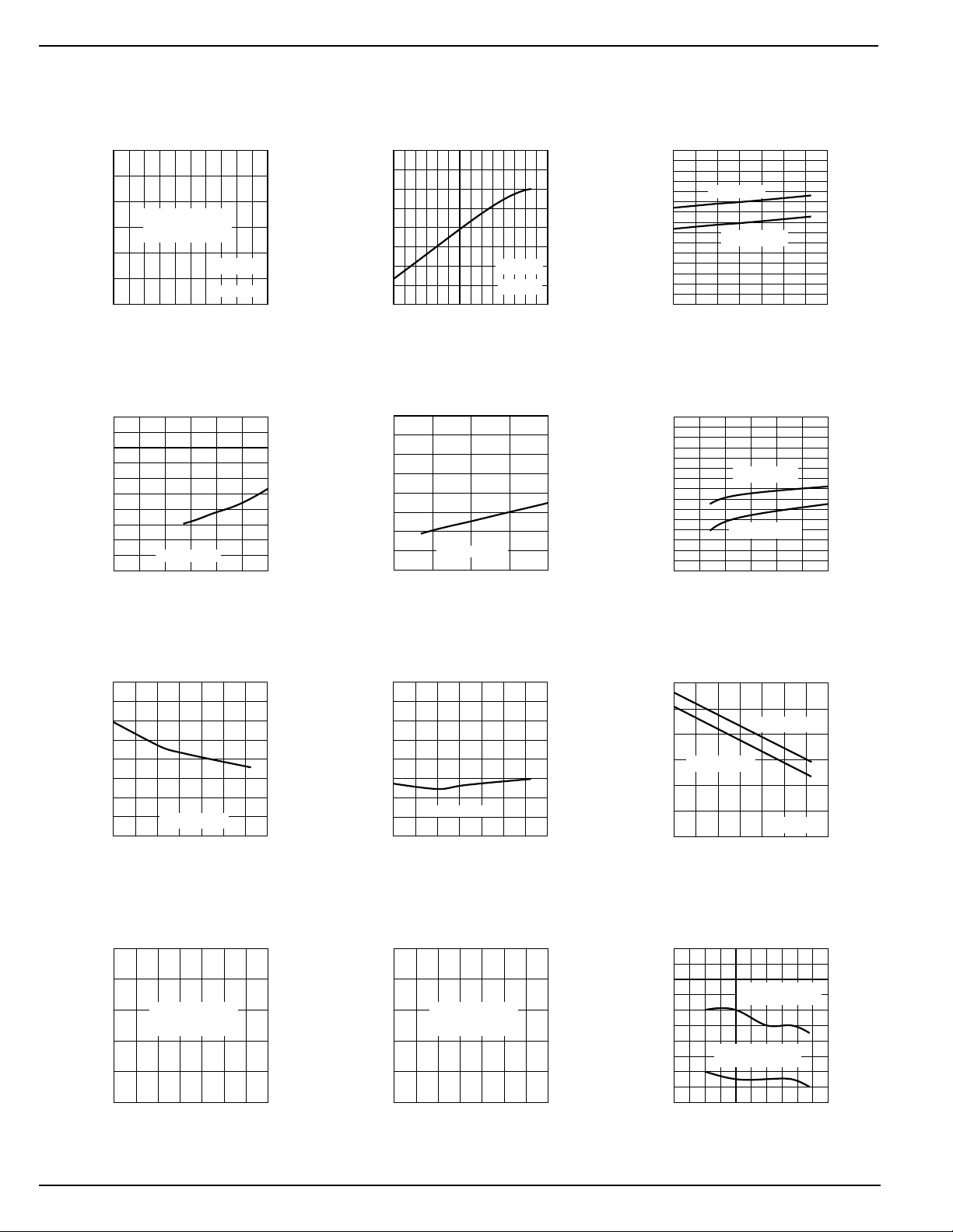
Typical Characteristics
VIN = 5V; TA = 25°C; one switch section; unless noted.
Output On-Resistance
vs. Supply Voltage
110
100
90
OUTPUT RESISTANCE (mΩ)
80
3.0 3.5 4.0 4.5 5 5.5
Awaiting Full
Characterization
Data
RL = 44Ω
T = 25°C
SUPPLY VOLTAGE (V)
On-State Supply Current
vs. Supply Voltage
250
200
150
100
50
SUPPLY CURRENT (µA)
0
0246
SWITCH ON
SUPPLY VOLTAGE (V)
Output On-Resistance
140
120
100
ON-RESISTANCE (mΩ)
vs. Temperature
80
60
-40 -20 0 20 40 60 80 100
TEMPERATURE (°C)
RL = 44Ω
VIN = 5V
Off-State Supply Current
vs. Supply Voltage
2.0
1.5
1.0
0.5
SUPPLY CURRENT (µA)
0
SWITCH OFF
23456
SUPPLY VOLTAGE (V)
UVLO Threshold Voltage
3.0
2.5
2.0
THRESHOLD VOLTAGE (V)
1.5
vs. Temperature
VIN RISING
VIN FALLING
-40 -20 0 20 40 60 80 100
TEMPERATURE (°C)
Control Threshold
vs. Supply Voltage
2.5
2.0
1.5
THRESHOLD VOLTAGE (V)
1.0
2345
V
RISING
CTL
V
FALLING
CTL
SUPPLY VOLTAGE (V)
On-State Supply Current
200
150
100
SUPPLY CURRENT (µA)
vs. Temperature
50
SWITCH ON
0
-40 -20 0 20 40 60 80 100
TEMPERATURE (°C)
Output Rise Time
vs. Temperature
5
4
3
2
TIME (µs)
1
0
-40 -20 0 20 40 60 80 100
Awaiting Full
Characterization
Data
TEMPERATURE (°C)
Off-State Supply Current
2.0
1.5
1.0
0.5
SUPPLY CURRENT (µA)
vs. Temperature
SWITCH OFF
0
-40 -20 0 20 40 60 80 100
TEMPERATURE (°C)
Output Fall Time
1.0
0.8
0.6
0.4
TIME (ms)
0.2
vs. Temperature
Awaiting Full
Characterization
Data
0
-40 -20 0 20 40 60 80 100
TEMPERATURE (°C)
Control Threshold
2.5
2.0
1.5
ENABLE VOLTAGE (V)
1.0
vs. Temperature
VEN RISING
VEN FALLING
VIN = 5V
-40 -20 0 20 40 60 80 100
TEMPERATURE (°C)
Current-Limit Threshold
2.0
1.8
1.6
1.4
CURRENT (A)
1.2
1.0
vs. Temperature
CURRENT LIMIT
THRESHOLD
SHORT CIRCUIT
CURRENT LIMIT
-25 0 25 50 75 100
TEMPERATURE (°C)
MIC2525 4 January 2000
 Loading...