

General Description
MIC2514
IttyBitty® Integrated High-Side Switch
Features
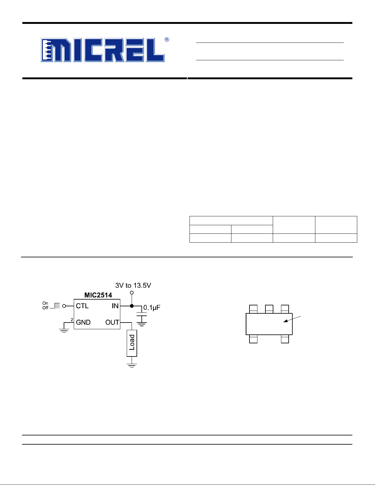
The MIC2514 is an integrated high-side power switch that
consists of a TTL compatible input and protected Pchannel MOSFET. The MIC2514 can be used instead of a
separate high-side driver and MOSFET in many lowvoltage applications.
The MIC2514 switches voltage ranging from 3V to 13.5V
and delivers more than 400mA continuous current. A slow
turn-on feature prevents high inrush current when
switching capacitive loads. The internal control circuitry is
powered from the unswitched 3V to 13.5V input.
• MOSFET on-resistance
– 1.5 typical at 5V
– 0.95 typical at 12V
• 3V to 13.5V input
• 25µA typical on-state supply current at 5V
• <1µA typical off-state supply current at 5V
• Current limit
• Thermal shutdown
• Slow turn-on
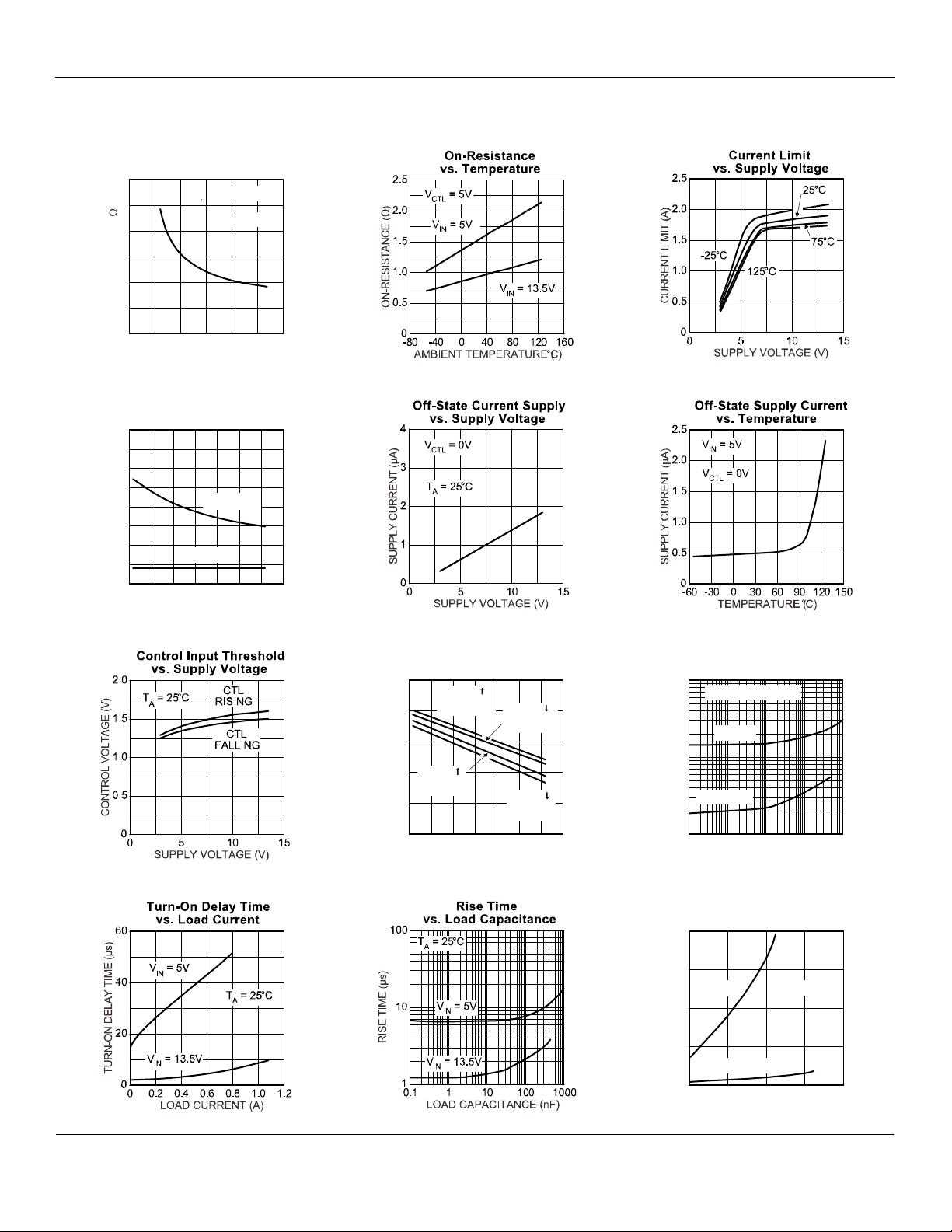
Current limiting is internally fixed at approximately 1.9A
and requires no external components.
Thermal shutdown turns off the output if the die
temperature exceeds approximately 170°C.
The MIC2514 is available in the 5-pin SOT-23-5 package
Applications
• 3.3V to 13.5V power management
Ordering Information
with a temperature range of –40°C to +85°C.
Datasheets and support documentation can be found on
Micrel’s web site at:www.micrel.com.
MIC2514BM5 MIC2514YM5 –40° to +85°C 5-Pin SOT-23
Part Number
Standard Pb-Free
Typical Application Pin Configuration
Temp. Range Package
1
High-Side Power Switch
3
4
IttyBitty is a registered trademark of Micrel, Inc.
Micrel Inc. • 2180 Fortune Drive • San Jose, CA 95131 • USA • tel +1 (408) 944-0800 • fax + 1 (408) 474-1000 • http://www.micrel.com
August 2008 1
GND
2
CTL
13
IN
F10
45
NCOUT
5-Pin SOT-23 (M5)
Part
Identification
M9999-082808-C
Micrel, Inc.
Pin Description
Pin Number Pin Name Pin Function
1 CTL Control (Input): Non-inverting TTL compatible control input. High = on, low = off.
2 GND Ground
3 IN
4 OUT Switch Output: Output MOSFET drain. Connect to switched side of load.
5 NC
Absolute Maximum Ratings
Supply Input: Output MOSFET source. Also supplies IC’s internal circuitry.
Connect to supply.
Not internally connected. Connect to ground plane for lowest package thermal
resistance.
(1)
Operating Ratings
(2)
MIC2514
Supply Voltage (VIN).....................................................+20V
Output Current (I
Control Input (V
Storage Temperature (T
). ................................ Internally Limited
OUT
) ......................................... –0.3V to 15V
CTL
).........................–65°C to +150°C
S
Supply voltage (VIN) ...................................... +3V to +13.5V
Ambient Temperature (T
) .......................... –40°C to +85°C
A
Junction Thermal Resistance
(θ
(θ
Control Input (V
) .................................................................220°C/W
JA
) .................................................................130°C/W
JC
)........................................... -0.3V to VIN
CTRL
Electrical Characteristics
V
= 5V; T
IN
Parameter Condition Min Typ Max Units
Supply Current
Output MOSFET
Resistance
Current Limit Threshold
General Note: Devices are ESD sensitive. Handling precautions recommended
Notes:
1. Exceeding the absolute maximum rating may damage the device.
2. The device is not guaranteed to function outside its operating rating.
3. Devices production tested at 25°C, but Devices guaranteed over indicated temperature range.
= 25°C, except bold values indicate –40°C< TA < +85°C, Note 3; unless noted.
A
V
= logic 0, VIN = 5V
CTL
= logic 0, VIN = 13.5V
V
CTL
V
= logic 1, VIN = 3V
CTL
= logic 1, VIN = 5V
V
CTL
V
= logic 1, VIN = 13.5V
CTL
V
= logic 0, 3V VIN 13.5V
CTL
= logic 1, 3V VIN 5V
V
CTL
= logic 1, 5V VIN 13.5V
V
CTL
VIN = 3V
VIN = 5V
= 12V
V
IN
V
= 3V
IN
V
= 5V
IN
= 12V
V
IN
0
0.8
0.8
1.0
1.2
0.6
2.0
10
25
95
1.45
1.65
2.4
1.5
0.95
0.5
1.4
1.9
10
25
20
40
200
0.79
2.0
2.3
4.5
2.4
2.7
1.5
1.7
1.5
2.0
2.5
µA
µA
µA
µA
µA
V Control Input Voltage
V
V
A
A
A
August 2008
2
M9999-082808-C
Micrel, Inc.
0
Typical Characteristics
On-Resistance
vs. Supply Voltage
3
(ECNATSISER-NO )
2
1
0
051015
SUPPLY VOLTAGE (V)
On-State S upply C urre nt
vs. Temperature
(TNERRUCYLPPUSµ)A
200
150
V
= 5V
CTL
TA = 25°C
MIC2514
100
50
0
-60 -30 0 30 60 90 120 150
TEMPERATURE (°C)
VIN = 13.5V
VIN = 5V
Control Input Thre s hold
vs. Temperature
2.5
2.0
)V(DLOHSERHT
1.5
1.0
0.5
V
=
CTL
VS = 13.5V
V
=
CTL
VIN = 5V
0
-60 -30 0 30 60 90 120 150
TEMPERATURE (°C)
V
=
CTL
VS = 13.5V
V
=
CTL
VIN = 5V
Turn-On Delay Ti me
vs. Loa d C apa c ita nc e
100
IL = 5mA, TA = 25°C
(EMITYALEDNO-NRUTµ)s
VIN = 5V
10
VIN = 13.5V
1
0.1 1 10 100 100
LOAD CAPACITANCE (nF)
Rise Time
vs. Load Current
80
August 2008
3
60
(EMITESIRµ)s
VIN = 5V
40
20
VIN = 13.5V
0
0 0.4 0.8 1.2 1.6
LOAD CURRENT (A)
TA = 25°C
M9999-082808-C

Micrel, Inc.
Typical Characteristics (continued)
Fall Ti me
vs. Load Capacitance
10
IL = 5mA, TA = 25°C
1
)sm(EMITLLAF
MIC2514
0.1
0.01
0.001
0.1 1 10 100 1000
VIN = 13.5V
VIN = 5V
LOAD CAPACITANCE (nF)
August 2008
4
M9999-082808-C

Micrel, Inc.
Functional Diagram
MIC2514
Functional Description
The MIC2514 is a non-inverting high-side switch. A
logic-high control input turns on the output transistor,
and a logic-low turns off the output transistor. Fault
conditions turn off the output transistor.
Control Input
Applying a logic-high input to CTL (control input)
activates the thermal shutdown and gate control circuits.
If there are no fault conditions, the output MOSFET turns
on.
Gate Control
The gate control circuit applies the supply voltage to the
output MOSFET gate, turning it off, or forces the
MOSFET gate below the supply voltage, turning it on, as
determined by CTL and thermal shutdown.
Input and Output
IN (input) is the supply connection to the logic circuitry
and the source of the output MOSFET. OUT (output) is
the drain of the output MOSFET. In a typical circuit;
current flows through the switch from IN to OUT toward
the load.
The output MOSFET has an intrinsic body diode which
will conduct if OUT is forced to a higher voltage than IN.
Thermal Shutdown
Thermal shutdown turns off the output MOSFET if the
die temperature exceeds approximately 170°C. Thermal
shut-down releases the output after the die temperature
decreases 10°C.
Current Limit
The current limit is preset internally. The preset level
prevents damage to the output MOSFET but allows a
typical current of 1.9A through the output MOSFET for
the MIC2514. This current limit is sufficient to protect the
bond wire and the output device from instantaneous high
current. Package thermal ratings and power dissipation
should be considered when determining safe continuous
operating current. Output current is monitored by
sensing the voltage drop across the output MOSFET
source metal resistance.
August 2008
5
M9999-082808-C

Micrel, Inc.
Package Information
MIC2514
5-Pin SOT-23 (M5)
MICREL, INC. 2180 FORTUNE DRIVE SAN JOSE, CA 95131 USA
TEL +1 (408) 944-0800 FAX +1 (408) 474-1000 WEB http:/www.micrel.com
The information furnished by Micrel in this data sheet is believed to be accurate and reliable. However, no responsibility is assumed by Micrel for its
Micrel Products are not designed or authorized for use as components in life support appliances, devices or systems where malfunction of a product
can reasonably be expected to result in personal injury. Life support devices or systems are devices or systems that (a) are intended for surgical implant
into the body or (b) support or sustain life, and whose failure to perform can be reasonably expected to result in a significant injury to the user. A
Purchaser’s use or sale of Micrel Products for use in life support appliances, devices or systems is a Purchaser’s own risk and Purchaser agrees to fully
use. Micrel reserves the right to change circuitry and specifications at any time without notification to the customer.
indemnify Micrel for any damages resulting from such use or sale.
© 1997 Micrel, Incorporated.
August 2008
6
M9999-082808-C

 Loading...