

Page 1
MIC24055 Evaluation Board
12A, High-Efficiency, Synchronous DC/DC
Buck Regulator with Hyper Speed Control™
Hyper Speed Control, SuperSwitcher II, and Any Capacitor are trademarks of Micrel, Inc.
Micrel Inc. • 2180 Fortune Drive • San Jose, CA 95131 • USA • tel +1 (408) 944-0800 • fax + 1 (408) 474-1000 • http://www.micrel.com
General Description
The MIC24055 DC/DC synchronous buck regulator operates
over an input supply range of 4.5V to 19V and provides a
regulated output at up to 12A of load current. The output
voltage is a djustabl e down to 0.8 V with a t ypical accur acy of
±1%. The device operates at a switching frequency of
600kHz, which remains relatively constant with changes in
input voltage and output load.
Micrel’s H yper Speed Control architecture allows for ultr afast transient response while reducing the output
capacitance. It also makes (High V
)/Low V
IN
possible. The 19V operating rating of the device provides
ample design safety margin for 12V input applications.
The MIC24055 utilizes an adaptive T
architecture. An undervoltage lockout feature is provided to
ensure proper operation under power-sag conditions. An
internal soft-start feature is provided to reduce the inrush
current. Fo ld b ac k current lim it an d “ h iccup” mode s hort-circuit
protection a nd th er mal shutd o wn e nsures prot ection of th e I C
during fault conditions.
The basic par ameters of the MIC2405 5 evaluation board are
a VIN supply of 5V to 19V, output voltage of 0.8V to 5V at
(1)
, and 600kHz switching frequency.
12A
Note:
1. Refer to the temperature curves present ed in the Evaluation Board
Performance section. Also, note that the typical minimum input
voltage to maximum output voltage conversion is limited by the
maximum duty cycle.
Datasheets and support documentation are available on
Micrel’s web site at: www.micrel.com
.
Requirements
The MIC24055 evaluation board requires only a single
power supply with at least 10A current capability. The
MIC24055 has internal VDD LDO so no external linear
regulator is require d to p o w er the i nter n al b iasi ng of th e IC .
When VIN < 5.5V, VDD should be tied to PVIN pins to
bypass the internal linear regulator by a jumper. The
output load can either be an active or passive load.
) operation
OUT
ripple control
ON
SuperSwitcher II™
Power-Up Precautions
The evaluation board does not have reverse polarity
protection. Appl ying a negative voltage t o the VIN terminal
may damage the device. The maximum VIN operating
voltage of the MIC24055 evaluation board is 19V. It has
two different layout designs, one (Figure 1) optimized for
evaluation and a seco nd (Figure 2) optim ized for a sm aller
footprint. The evaluation board is only populated with
components shown in Figure 1.
Getting Started
1. VIN Supply.
Connect a supply to the VIN and GND terminals,
paying careful attention to the polarity and the supply
range (5V < VIN < 19V). An ammeter may be placed
between the input supply and the VIN terminal to the
evaluation board. Ensure that the supply voltage is
monitored at the VIN terminal. The ammeter and/or
power lead resistance can reduce the voltage supplied
to the input. Do not apply power until Step 4.
2. Connect the load to the VOUT and ground
terminals.
The load can be either passive (resistive) or active (as
in an electronic load). An ammeter can be placed
between the load and the VOUT terminal. Ensure that
the output voltage is monitored at the VOUT terminal.
3. Enable Input.
An EN connector is pro vide d on the eval uat ion bo ard
for users to easily access the enable feature. The
output of the MIC24055 turns on when VDD
exceeds
the UVLO threshold. The output of the MIC24055 may
be turned off by shorting the EN pin to ground.
4. Turn on the power.
Turn on VIN power supply and verify that the output
voltage is regulated to 1.8V.
Ordering Information
Part Number Description
MIC24055YJL EV
12A HSC DC/DC Buck Regulator
Evaluation Board
February 11, 2013
Revision 1.0
Page 2

Micrel, Inc.
MIC24055 Evaluation Board
February 11, 2013
+×=
BOTTOM
FB
OUT
R
R4
1VV
FB
OUT
FB
BOTTOM
VV
VR4
R
−
×
=
0.8VV
0.8V R4
R
OUT
BOTTOM
−
×
=
Output Voltage
The output voltage on the MIC24055 evaluation board is
adjustable. It is set b y adjusting the feed back resistor s, as
illustrated in Equation 1:
Eq. 1
where V
= 0.8V and R
FB
is one of the R5, R6, R7,
BOTTOM
R8, R9, R10, R11, R12 which corresponds to 0.9V, 1.0V,
1.2V, 1.5V, 1.8V, 2.5V, 3. 3V, or 5V. Leaving the R
BOTTOM
open gives a 0.8V output voltage. The output voltage
above is set at the factory for a 1.8V output, but it can
easily be changed by moving the jumper to a respective
position to get an indicated voltage on the board. If a
desired voltage is not shown on the board, it is easily
modified by removing R
and replacing it with the
BOTTOM
values that yield the desired output voltage. Once R4 is
selected, R
can be calculated using Equ ati on 2:
BOTTOM
Eq. 2
For V
= 0.8V, as in Equation 3:
FB
Eq. 3
The output voltage should not be set to exceed 5V due to
the 6.3V rating of the output capacitor and limitation on line
regulation. Please r efer to t he “Setting the Outp ut Volt age”
and Ripple Injection” subsections in the Application
Information section of the MIC24 055 data sheet for m ore
detailed information.
2
Revision 1.0
Page 3
Micrel, Inc.
MIC24055 Evaluation Board
February 11, 2013
50
55
60
65
70
75
80
85
90
95
100
0 3 6 9 12 15
EFFICIENCY (%)
OUTPUT CURRENT (A)
Efficiency (VIN = 5V)
vs. Output Current
3.3V
2.5V
1.8V
1.5V
1.2V
1.0V
0.9V
0.8V
VIN = 5V
50
55
60
65
70
75
80
85
90
95
100
0 3 6 9 12 15
EFFICIENCY (%)
OUTPUT CURRENT (A)
Efficiency (VIN = 12V)
vs. Output Current
5.0V
3.3V
2.5V
1.8V
1.5V
1.2V
1.0V
0.9V
0.8V
VIN = 12V
0
20
40
60
80
100
0 2 4 6 8 10 12
DIE TEMPERATURE (°C)
OUTPUT CURRENT (A)
Die Temperature* (VIN = 5V)
vs. Output Current
VIN = 5V
V
OUT
= 1.8V
0
20
40
60
80
100
0 2 4 6 8 10 12
DIE TEMPERATURE (°C)
OUTPUT CURRENT (A)
Die Temperature* (VIN = 12V)
vs. Output Current
VIN = 12V
V
OUT
= 1.8V
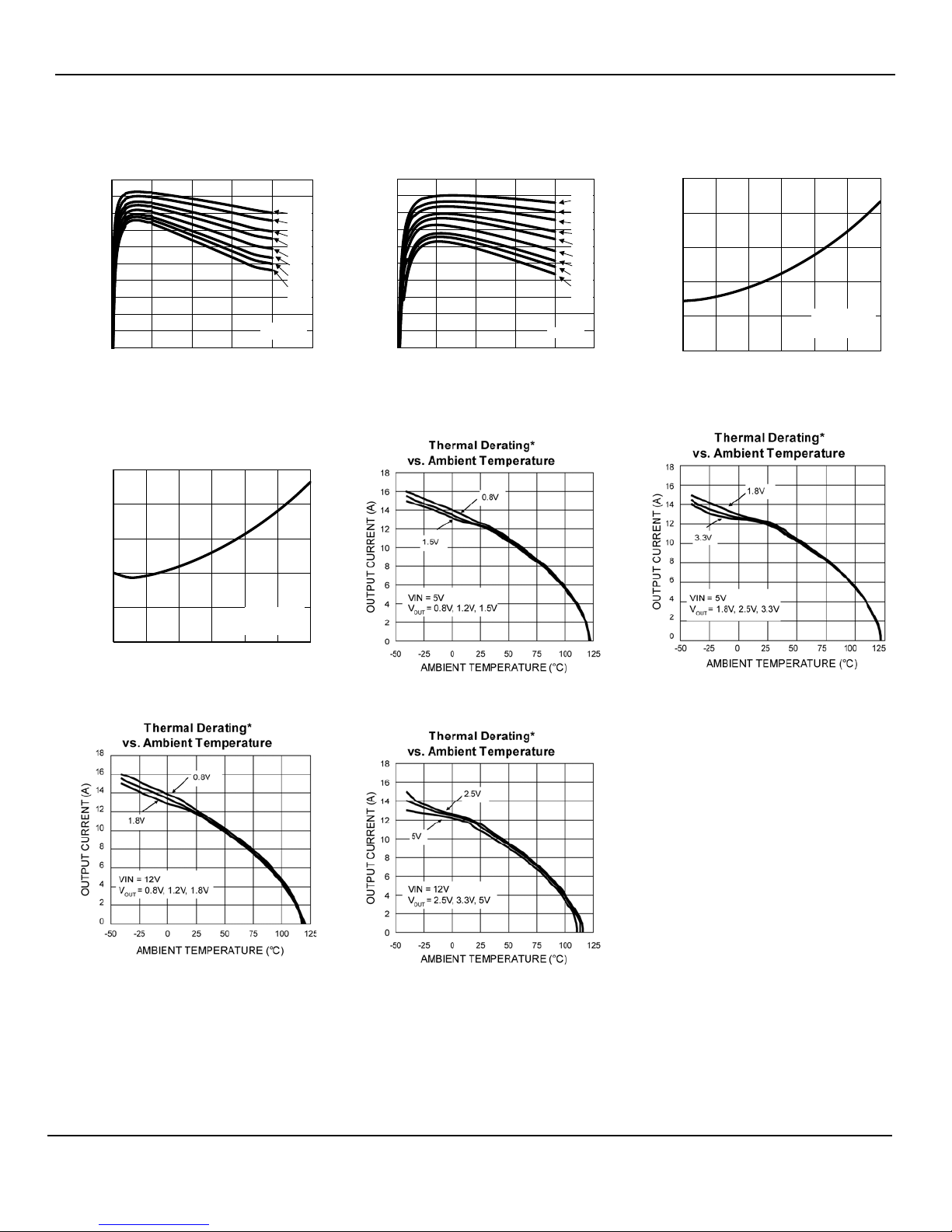
Evaluation Board Performance
Die Temperature* : The temperature m easurement was taken at the hottest point on the MIC24055 case mounted on a 5 square inch 4 layer, 0.62 inch,
FR-4 PCB with 2oz finish copper weight per layer, see the Thermal Measurement section in the MIC24055 datasheet. A ctual results will depend upon
the size of the PCB, ambient temperature and proximity to other heat-emitting components.
3
Revision 1.0
Page 4
Micrel, Inc.
MIC24055 Evaluation Board
February 11, 2013
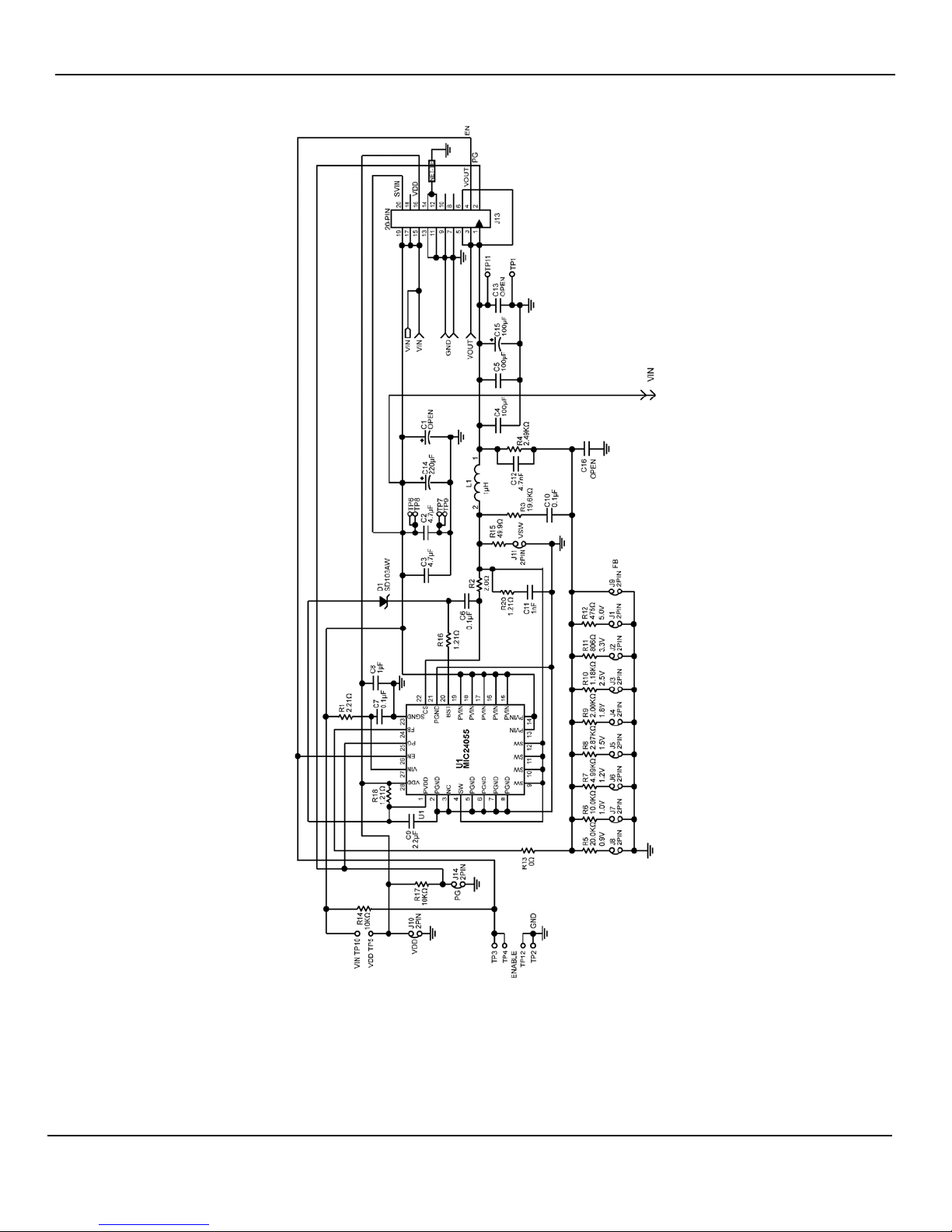
Evaluation Board Schematic
Figure 1. Schematic of MIC24055 Evaluation Board
4
(J11, R13, and R15 are for testing purposes)
Revision 1.0
Page 5
Micrel, Inc.
MIC24055 Evaluation Board
February 11, 2013
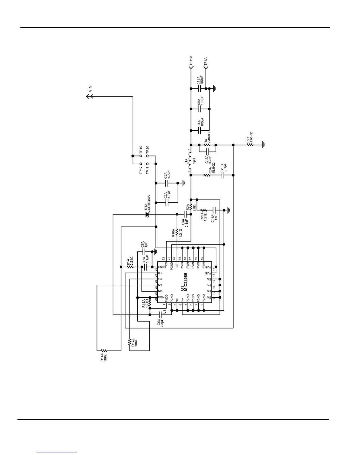
Evaluation Board Schematic (Continued)
Figure 2. Schematic of MIC24055 Evaluation Board − Optimized for Smaller Footprint
5
(J11, R13, and R15 are for testing purposes)
Revision 1.0
Page 6
Micrel, Inc.
MIC24055 Evaluation Board
February 11, 2013
12103C475KAT2A
AVX
(1)
GRM32DR71E475KA61K
Murata
(2)
C3225X7R1E475K
TDK
(3)
12106D107MAT2A
AVX
GRM32ER60J107ME20L
Murata
C3225X5R0J107M
TDK
C15
Open
06035C104KAT2A
AVX
GRM188R71H104KA93D
Murata
C1608X7R1H104K
TDK
0603ZC105KAT2A
AVX
GRM188R71A105KA61D
Murata
C1608X7R1A105K
TDK
0603ZD225KAT2A
AVX
GRM188R61A225KE34D
Murata
C1608X5R1A225K
TDK
06035C472KAZ2A
AVX
GRM188R71H472K
Murata
C1608X7R1H472K
TDK
C14
B41851F7227M
EPCOS
(4)
220µF Aluminum Capacitor, 35V
1
C11, C16
Open
SD103AWS
MCC
(5)
SD103AWS-7
Diodes Inc
(6)
SD103AWS
Vishay
(7)
L1
HCF1305-1R0-R
Cooper Bussmann
(8)
1.0µH Inductor, 21A Saturation Current
1
R1
CRCW06032R21FKEA
Vishay Dale
2.21Ω Resistor, Size 0603, 1%
1
R2
CRCW06032R00FKEA
Vishay Dale
2.00Ω Resistor, Size 0603, 1%
1
R3
CRCW060319K6FKEA
Vishay Dale
19.6kΩ Resistor, Size 0603, 1%
1
R4
CRCW06032K49FKEA
Vishay Dale
2.49kΩ Resistor, Size 0603, 1%
1
R5
CRCW060320K0FKEA
Vishay Dale
20.0kΩ Resistor, Size 0603, 1%
1
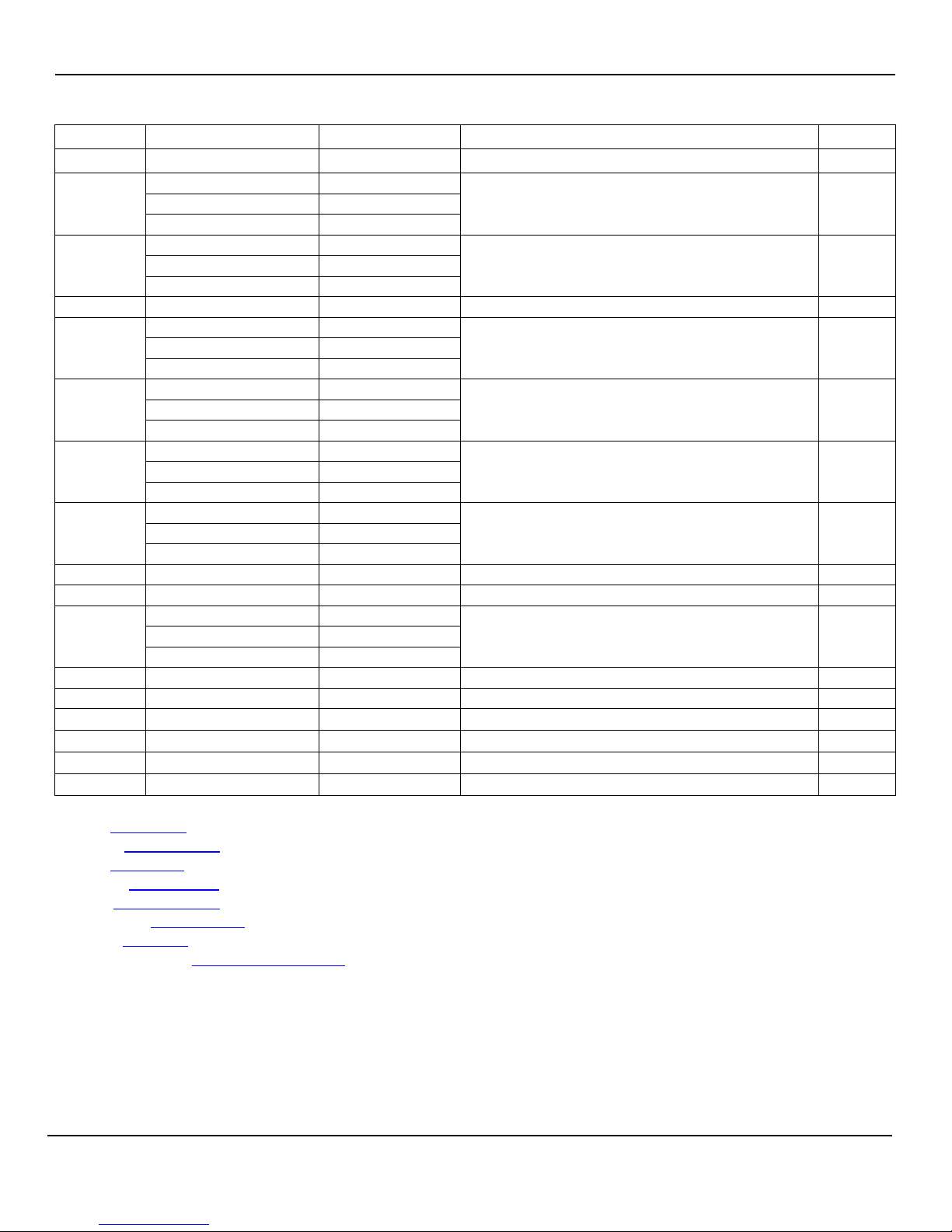
Bill of Materials
Item Part Number Manufacturer Description Qty.
C1 Open
C2, C3
C4, C5, C13
C6, C7, C10
C8
C9
C12
D1
4.7µF Ceramic Capacitor, X7R, Size 1210, 25V 2
100µF Ceramic Capacitor, X5R, Size 1210, 6.3V 3
0.1µF Ceramic Capacitor, X7R, Size 0603, 50V 3
1.0µF Ceramic Capacitor, X7R, Size 0603, 10V 1
2.2µF Ceramic Capacitor, X5R, Size 0603, 10V 1
4.7nF Ceramic Capacitor, X7R, Size 0603, 50V 1
40V, 350mA, Schottky Diode, SOD323 1
Notes:
1. AVX: www.avx.com
2. Murata: www.murata.com.
3. TDK: www.tdk.com.
4. EPCOS: www.epcos.com.
5. MCC: www.mccsemi.com.
6. Diodes, Inc.: www.diodes.com.
7. Vishay: www.vishay.
8. Cooper Bussmann.: www.cooperbussmann.com.
.
6
Revision 1.0
Page 7
Micrel, Inc.
MIC24055 Evaluation Board
February 11, 2013
R6, R14, R17
CRCW060310K0FKEA
Vishay Dale
10.0kΩ Resistor, Size 0603, 1%
3
R7
CRCW06034K99FKEA
Vishay Dale
4.99kΩ Resistor, Size 0603, 1%
1
R8
CRCW06032K87FKEA
Vishay Dale
2.87kΩ Resistor, Size 0603, 1%
1
R9
CRCW06032K006FKEA
Vishay Dale
2.00kΩ Resistor, Size 0603, 1%
1
R10
CRCW06031K18FKEA
Vishay Dale
1.18kΩ Resistor, Size 0603, 1%
1
R11
CRCW0603806RFKEA
Vishay Dale
806Ω Resistor, Size 0603, 1%
1
R12
CRCW0603475RFKEA
Vishay Dale
475Ω Resistor, Size 0603, 1%
1
R13
CRCW06030000FKEA
Vishay Dale
0Ω Resistor, Size 0603, 5%
1
R15
CRCW060349R9FKEA
Vishay Dale
49.9Ω Resistor, Size 0603, 1%
1
R16, R18
CRCW06031R21FKEA
Vishay Dale
1.21Ω Resistor, Size 0603, 1%
2
R20
Open
All Reference
with “A”
12A, High-Efficiency, Synchronous DC/DC Buck
Regulator with Hyper Speed Control
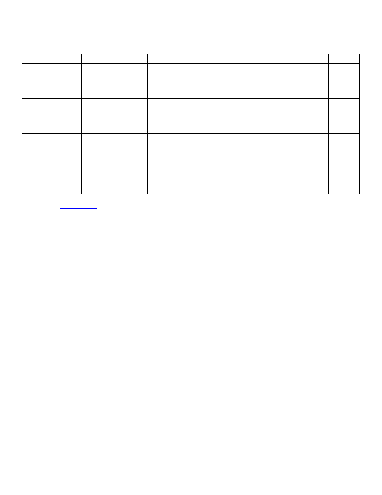
Bill of Materials (Continued)
Item Part Number Manufacturer Description Qty.
designators ending
Open
U1 MIC24055YJL Micrel. Inc.
Note:
9. Micrel, Inc.: www.micrel.com
.
(9)
1
7
Revision 1.0
Page 8
Micrel, Inc.
MIC24055 Evaluation Board
February 11, 2013
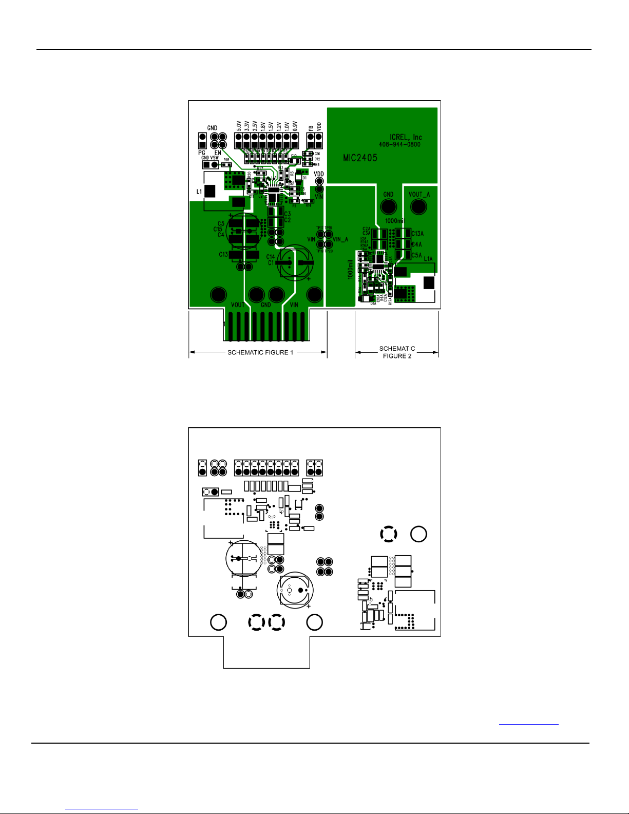
PCB Layout Recommendations
(1)
Top Layer
Note:
1. Refer to “PCB Layout Guideline” section for component placement and layout in MIC24055 datasheet on Micrel web page (www.micrel.com
8
Mid-Layer 1 (Power Ground Plane
)
Revision 1.0
Page 9
Micrel, Inc.
MIC24055 Evaluation Board
February 11, 2013
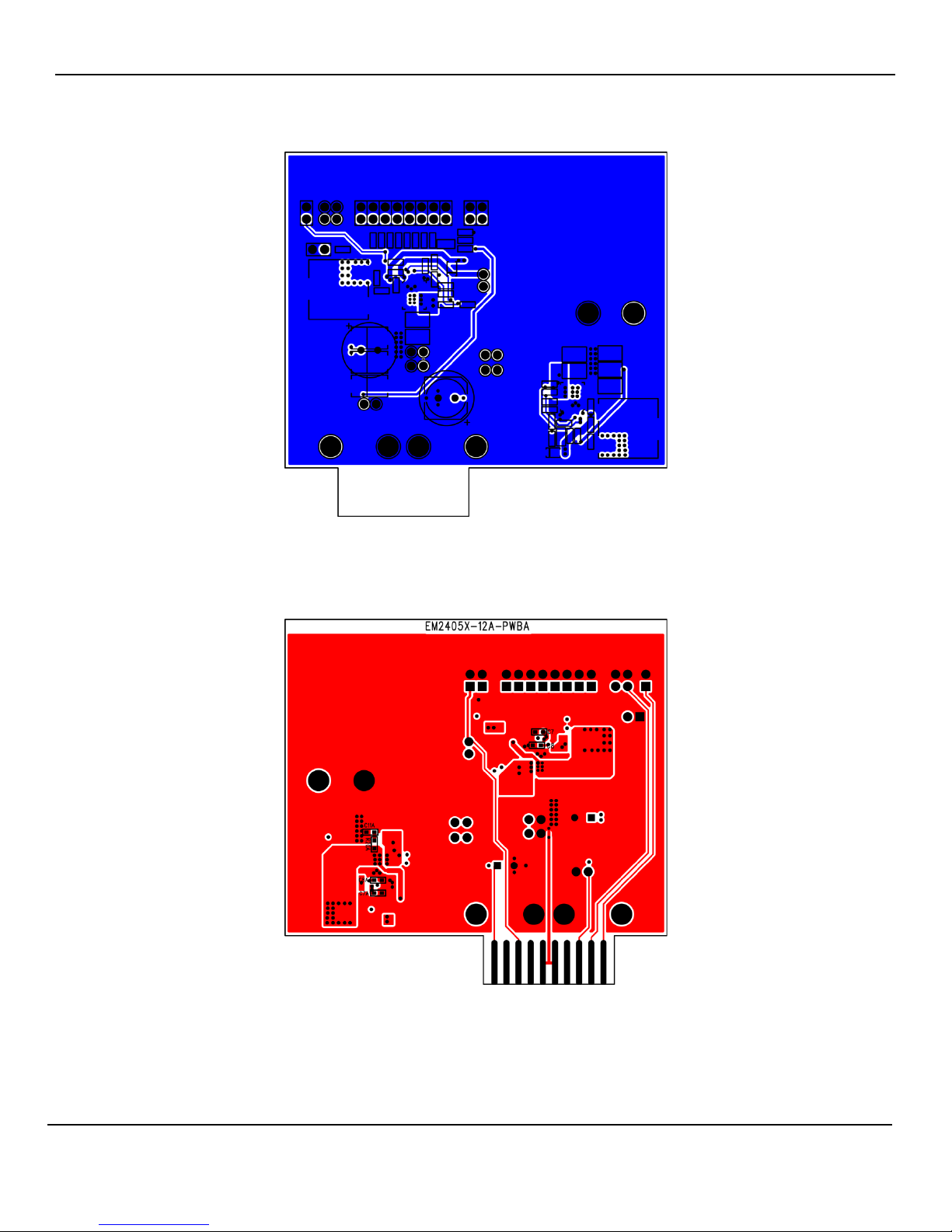
PCB Layout Recommendations
(1)
(Continued)
Mid-Layer 2
9
Bottom Layer
Revision 1.0
Page 10

Micrel, Inc.
MIC24055 Evaluation Board
February 11, 2013
MICREL, INC. 2180 FORTUNE DRIVE SAN JOSE, CA 95131 USA
significant injury to the user. A
icrel Products for use in life support appliances, devices or systems is a Purchaser’s own risk and Purchaser agrees to fully
TEL +1 (408) 944-0800 FAX +1 (408) 474-1000 WEB http://www.micrel.com
Micrel makes no representations or warranties with respect to the accuracy or completeness of the information furnished in this data sheet. This
information is not intended as a warranty and Micrel does not assume responsibility for its use. Micrel reserves the right to change circuitry,
specifications and descriptions at any time without notice. No license, whether express, implied, arisi ng by estoppel or ot herwise, to any intellectual
property rights is granted by this document. Except as provided in Micrel’s terms and conditions of sale for such products, Micrel assumes no liability
whatsoever, and Micrel disclaims any express or implied warranty relating to the sale and/or use of Micrel products including liability or warranties
relating to fitness for a particular purpose, merchantability, or infringement of any patent, copyright or other intellectual property right.
Micrel Products are not designed or authorized for use as components in life support appliances, devices or systems where malfunction of a product
can reasonably be expected to result in personal injury. Life support devices or systems are devices or systems that (a) are intended for surgical
implant into the body or (b) support or sustain life, and whose failure to perform can be reasonably expected to result in a
Purchaser’s use or sale of M
indemnify Micrel for any damages resulting from such use or sale.
10
© 2013 Micrel, Incorporated.
Revision 1.0
 Loading...