

Page 1

Single AA/AAA Cell Step-Up/Step-Down
Regulators with Battery Monitoring
General Description
MIC23099 Evaluation Board
Getting Started
The MIC23099 is a hi gh-efficien cy, low-noise, dual-output,
integrated power-management solution for single-cell
alkaline or NiMH battery applications. The synchronous
boost output voltage (V
) is enabled first and is
OUT1
powered from the battery. Next, the synchronous buck
output (V
voltage − is enabled. This configuration allo ws V
) − which is powered from the boost output
OUT2
OUT2
t o be
independent of batter y vo ltage, thereby allowing the buck
output voltage to be higher or lower than the battery
voltage.
To minimize switching ar tifacts in th e audio band, both the
converters are design t o o p er ate with a minimum switchin g
frequency of 80k Hz f or t he buck and 10 0k Hz for th e boost .
The high current boost has a maximum switching
frequency of 1MHz, minimizing the solution foot-print.
The MIC23099 incorporates both battery-management
functions and fault protection. The low-battery level is
indicated by an external LE D connected to the LED pin. In
addition, a supervisory circuit monitors each output and
asserts a power-good ( PG) signal when the s equencing is
done or de-asserted when a fault condition occurs.
The basic parameters of the evaluation board are:
• Input: 0.85V to 1.6V
• Output 1: 1.8V/0.2A
• Output 2: 1.0V/30mA
Datasheets and support documentation are available on
Micrel’s web site at: www.micrel.com
.
Requirements
The MIC23099 evaluation board requires only a single
power supply with at least 1A current capability. The
output load can either be an active (electronic ) or passive
(resistive) load.
Precautions
The MIC23099 evaluation board does not have reverse
polarity protection. Applying a negative voltage to the VIN
and GND terminals may damage the device. The
maximum oper ating rating for V
is 1.6V. Excee ding 1.6V
IN
on the VIN could damage the device.
1. VIN Supply
Connect a supply to the VIN and GND terminals,
paying careful att ention to the polarity and t he supply
range (0V < VIN < 1. 6 V) . D o not app ly power until step
4.
2. Connect Load and Monitor Output
Connect a load to the VOUT1 and VOUT2 an d GND
terminals. The load can be either a passive (resistive)
or an active (as in an e lectronic load) type. A current
meter may be placed between the output terminals
and load to monitor the out put current. Ensure that the
output voltage is monitored at the output terminals.
3. Enable Input
The EN pin has an internal 4MΩ pull-down r esistor to
GND, which allows the output to be turned off when
the EN jumper is rem oved. Applying an externa l logic
signal on the EN pi n to p ull it high or using a jum per to
short the EN pin to VIN to turn the outputs on.
4. Turn Power
Turn on the VIN supply and verify that the output
voltages VOUT1 = 1.8V and VOUT2 = 1.0V.
5. Power Good Output
This is on open dr ain output that is pulled high when
, V
V
IN
and V
FB1
are within their nominal voltage
FB2
levels. The power good wil l be pulle d lo w w ith out d el a y
when the enable pin is set low.
6. LED Output
This is an open drain output that is used for a low
battery indicator. Under no rmal conditions, the LED is
always ON. If the battery voltage is between 1.2V to
0.85V, the external L ED will blink with a dut y cycle of
25% at 0.25Hz. The LED will be OFF if the battery
voltage falls below 0.85V for more than 15 cool-off
cycles or the EN pin is low.
7. SW1 and SW2 Test Points
These are switch node test points.
Ordering Information
Part Number Description
MIC23099YFT EB MIC23099 Evaluation Board
HyperLight Load is a registered trademark and Hyper Speed Control is a trademark of Micrel, Inc.
Micrel Inc. • 2180 Fortune Drive • San Jose, CA 95131 • USA • tel +1 (408) 944-0800 • fax + 1 (408) 474-1000 • http://www.micrel.com
May 30, 2014
Revision 1.0
Page 2
Micrel, Inc.
MIC23099 Evaluation Board
−
=
1
V6.0
V
1R
2R
OUT
Evaluation Board Features
Feedback Resistors
An external resistive di vider network (R1 and R2) with its
center tap connected to the feedback pin sets the output
voltage for each regu lator. R1 is t he top resist or and R2 is
the bottom resis tor in t h e d i vider str i ng. The resistor values
for the desired output voltage are calculated as illustr ated
in Equation 1. Large resistor values are rec ommended to
reduce light load operat ing c urrent, and im prove eff icienc y.
The recommended resistor value for R1 sho uld be ar ound,
R1 ≈ 400kΩ.
Eq. 1
In the case of the boost converter, Equation 1 sets the
output voltage to its PW M value. The no-load PFM output
voltage is 2% higher than the PWM value. This higher
PFM output voltag e value is necessary to prevent PF M to
PWM mode skipping which can introduce noise into the
audio band.
Boost Switching Frequency
To reduce switching artif acts in the audio band, the buck
and boost regulators s witching frequency are contr olled to
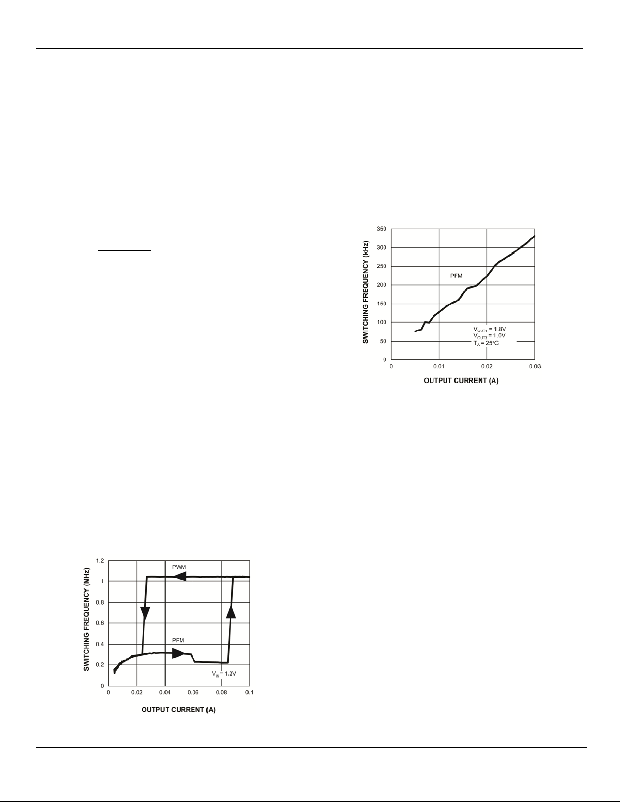
minimize overlap. Figure 1 shows the boost switching
frequency versus output load current and Figure 2 shows
the buck switching frequency versus output load current.
The boost regulator oper a t es in eith er PWM or PFM mode.
To avoid PWM to PFM chatter, the PWM entry and exit
points are not the same. When in PFM mode the output
current needs to reach 90 m A to enter into PWM mode and
exits at 30mA. The boost switching frequency is greater
than 100kHz with loads greater than 20mW.
Buck Switching Frequency
The buck converter is designed to operate in PFM mode
only. It has peak current control, which turns off the highside switch when the inductor current hits the current limit
threshold. The c ycle repeat s itself when the output v oltage
falls below its regulated value. As a result, the switching
frequency varies linearly with output current as shown in
Figure 2. The buck switching frequency is greater than
80kHz with loads greater than 8mW.
Figure 2. Buck Switching Frequency vs. Output Current
Power Good
The power good (PG) circu itr y monitors the batter y voltage
and feedback pin v olt ag e o f the b oos t and buc k regulators.
The PG pin output goes logic high when F B1 and FB2 pin
voltages are both greater than 92.5% (typical) of the
internal reference voltage and the input voltage is greater
than 0.85V (typical). To minimize false triggering, the
power-good output has both a turn on delay and a f alling
deglitch delay.
Figure 1. Boost Switching Frequency vs. Output Current
May 30, 2014 2
Revision 1.0
Page 3
Micrel, Inc.
MIC23099 Evaluation Board
Low-Battery Detection and Output Latch-Off
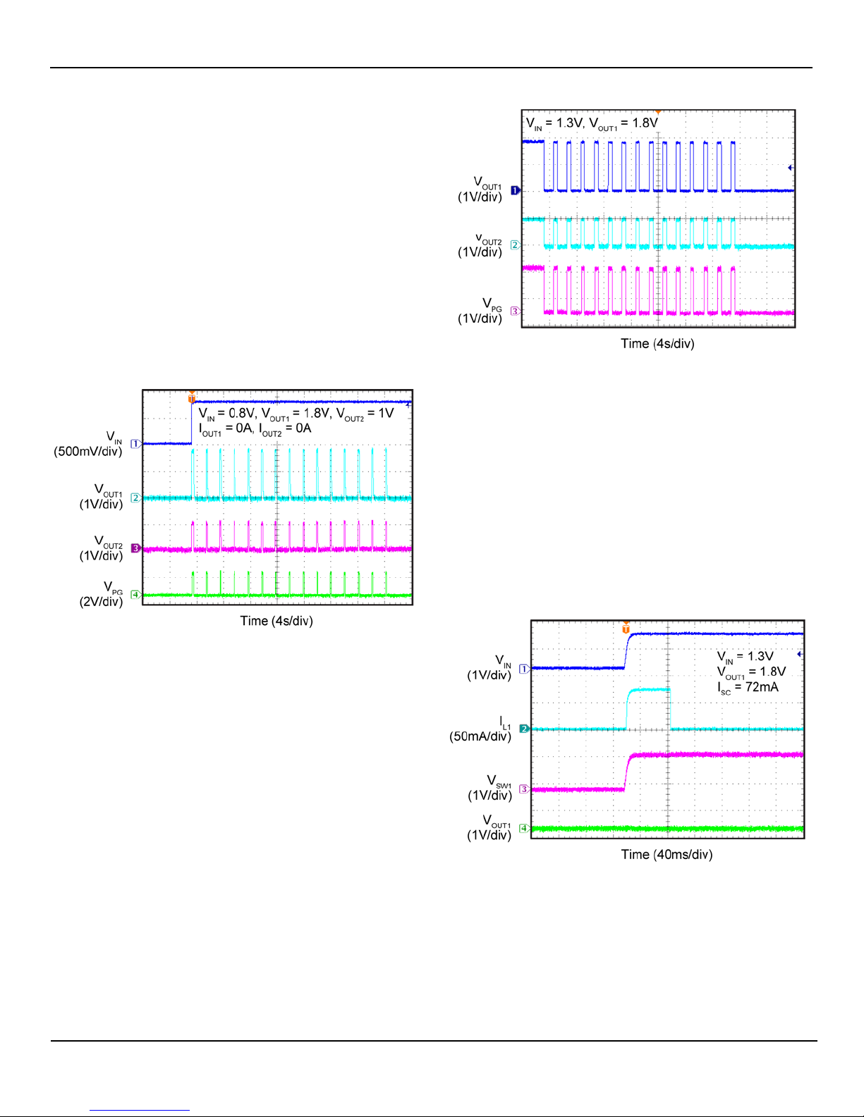
Figure 3 shows the low-battery power cycling operatio n. If
the battery voltage (V
) drops bel ow 0.85V for more than
IN
100ms to 150ms, the PG de-asserts (goes low) and
outputs V
OUT1
and V
active discharges resistors are enabled, discharges V
and V
to ground and finally the MIC23099 enters a
OUT2
are disabled. Then the 500Ω
OUT2
OUT1
cool off or sleep period. After a cool off period of abou t 1.3
seconds, if the battery voltage is above the 0.85V
threshold, then the outputs will power up again. This cycle
repeats itself until the end of the 15
th
cycle when both
outputs are latched off for the last time.
The outputs can be t urned back on by recycling th e input
power or by toggling the enab le pin. If the battery voltage
is still low, the MIC23099 wil l turn itself off again after 15
power-up cycles.
Figure 4. Output Fault Power Cycling
Boost Short-Circuit Protection
The low-side current limit protects the IC from transientoverload conditions, bu t not from a direct short-to-ground.
The high-side MOSFET current limit provides the
protection from a short-to-ground. In this fault condition,
the high-side PMOS switch operates in linear mode and
limits the current to approxi mately 80mA. If the short-circuit
condition last for more than 30ms, the PMOS switch is
latched off as shown in Figur e 5. The outputs are not reenabled until the input p ower is recycled or the enable pin
is toggled.
Figure 3. Low-Battery Power Cycling
Output Fault and Power Cycling
If either V
OUT1
or V
outputs are out of tolerance for
OUT2
longer than the power good deglitch delay of between
60ms to 120ms, then both outputs are disabled. The
power-down procedure is the sam e as the low-batter y f ault
detection, as shown in Figure 3. The outputs can be turned
back on by recycling the input power or by toggling the
enable pin. The latch-off feature eliminates the thermal
stress on the MIC23099 a nd the external inductors d uring
a fault event.
Figure 5. Power-Up into Short Circuit
May 30, 2014 3
Revision 1.0
Page 4

Micrel, Inc.
MIC23099 Evaluation Board
Boost Overcurrent Protection
The boost converter has current-limit protection on both
the high-side and low-side MOSFETs. The low-side
MOSFET provides cycle-by-cycle current limiting. When
the peak switch current exceeds the NMOS current limit
threshold, then the low-side switch is immediately turned
off and the high-side switch is turned on. Peak switch
current is limited to approximately 1.5A. The low-side
switch is allowed to tur n on again on th e next clock c ycle.
If the overload cond ition lasts more than 6 0ms to 120ms,
then both ou tputs are disa bled and the IC enters its power
cycling mode.
May 30, 2014 4
Revision 1.0
Page 5
Micrel, Inc.
MIC23099 Evaluation Board
40
50
60
70
80
90
100
0.001 0.01 0.1
EFFICIENCY (%)
OUTPUT CURRENT (A)
Efficiency (VIN= 1.2V)
vs. Output Current
BOOST
V
OUT1
= 1.8V
BUCK
V
OUT2
= 1.0V
LED PIN = OPEN
L1 = IFSC1515AHER6R8M01
L2 = SPM4012T-4R7M
0.2
40
50
60
70
80
90
100
0.001 0.01
EFFICIENCY (%)
OUTPUT CURRENT (A)
Buck Efficiency (VIN= 1.8V)
vs. Output Current
VIN= 1.8V
V
OUT2
= 1.0V
TA= 25⁰C
L2 = SPM4012T-4R7M
L2 = CIG2MW4R7NNE
0.03
0.97
0.98
0.99
1
1.01
1.02
1.03
0 0.01 0.02 0.03
OUTPUT VOLTAGE (V)
OUTPUT CURRENT (A)
Buck Output Voltage
vs. Output Current
VIN= 1.8V
V
OUT2
= 1.0V
TA= 25⁰C
PFM
-1.0%
-0.5%
0.0%
0.5%
1.0%
0 0.01 0.02 0.03
LOAD REGULATION (%)
OUTPUT CURRENT (A)
Buck Load Regulation
vs. Output Current
VIN= 1.8V
V
OUT2
= 1.0V
TA= 25⁰C
PFM
0.598
0.600
0.602
0.604
0.606
0.608
0.610
0.612
0.614
-50 -25 0 25 50 75 100 125
FEEDBACK VOLTAGE (V)
TEMPERATURE (°C)
Boost Feeback Voltage
vs. Temperature
VIN= 1.2V
TA= 25⁰C
PFM
I
OUT1
= 100uA
PWM
I
OUT1
= 100mA
-4.0%
-2.0%
0.0%
2.0%
0 0.04 0.08 0.12 0.16 0.2
LOAD REGULATION (%)
OUTPUT CURRENT (A)
Boost Output Voltage
vs. Output Current
VIN= 1.2V
V
OUT1
= 1.8V
TA= 25⁰C
PFM
PWM
1.75
1.76
1.77
1.78
1.79
1.80
1.81
1.82
1.83
1.84
0 0.04 0.08 0.12 0.16 0.2
OUTPUT VOLTAGE (V)
OUTPUT CURRENT (A)
Boost Output Voltage
vs. Output Current
VIN= 1.2V
V
OUT1
= 1.8V
TA= 25⁰C
PWM
PFM
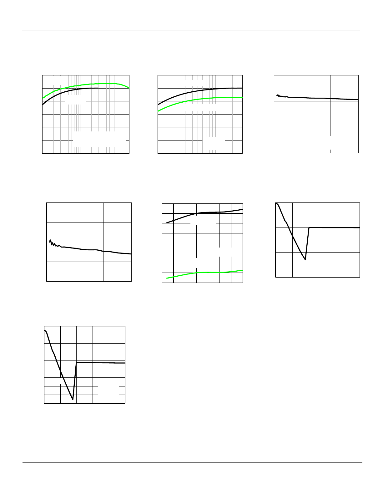
Typical Characteristics
May 30, 2014 5
Revision 1.0
Page 6
Micrel, Inc.
MIC23099 Evaluation Board
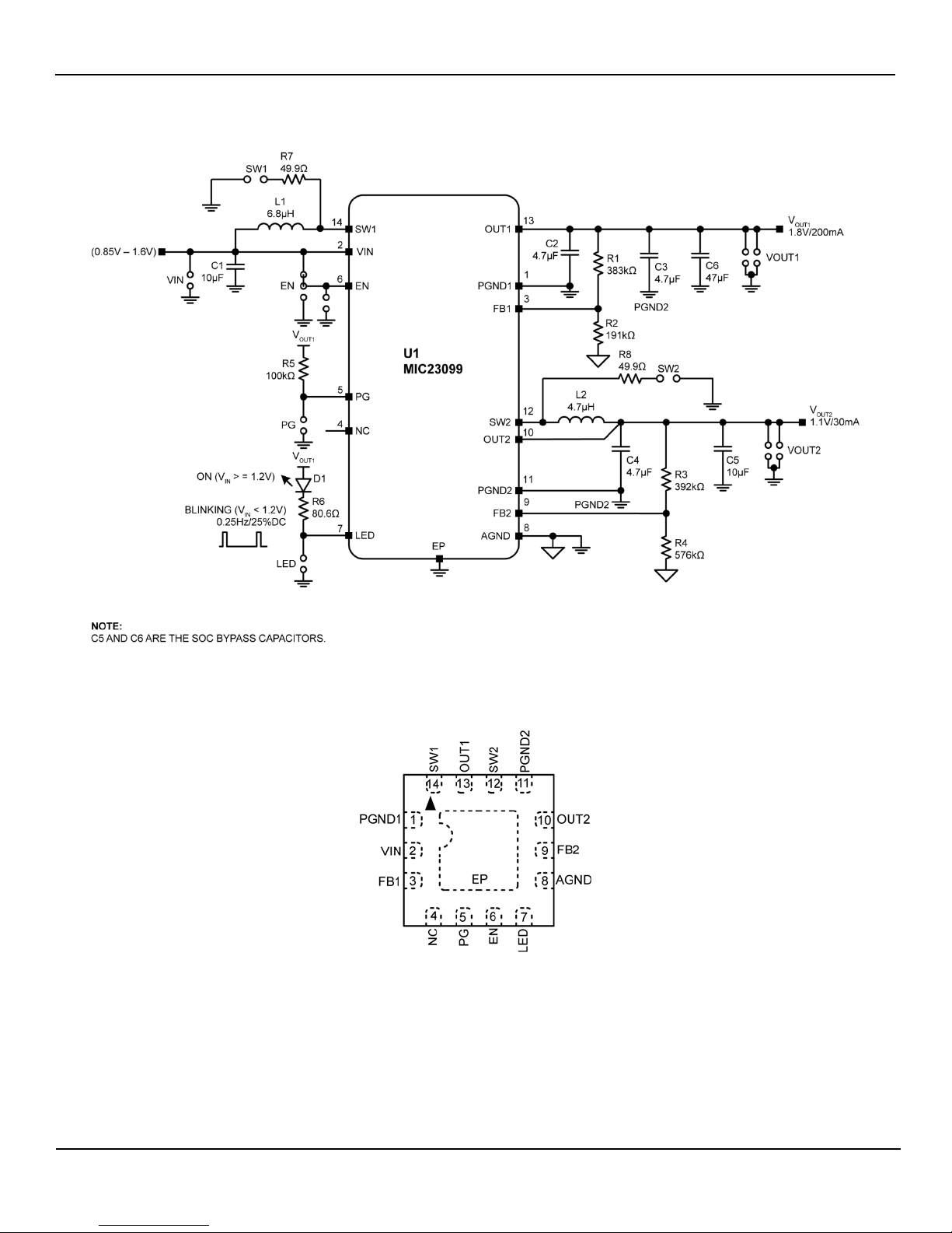
Typical Application Schematic
Pin Configuration
14-Pin 2.5mm × 2.5mm QFN (YFT)
(Top View)
May 30, 2014 6
Revision 1.0
Page 7
Micrel, Inc.
MIC23099 Evaluation Board
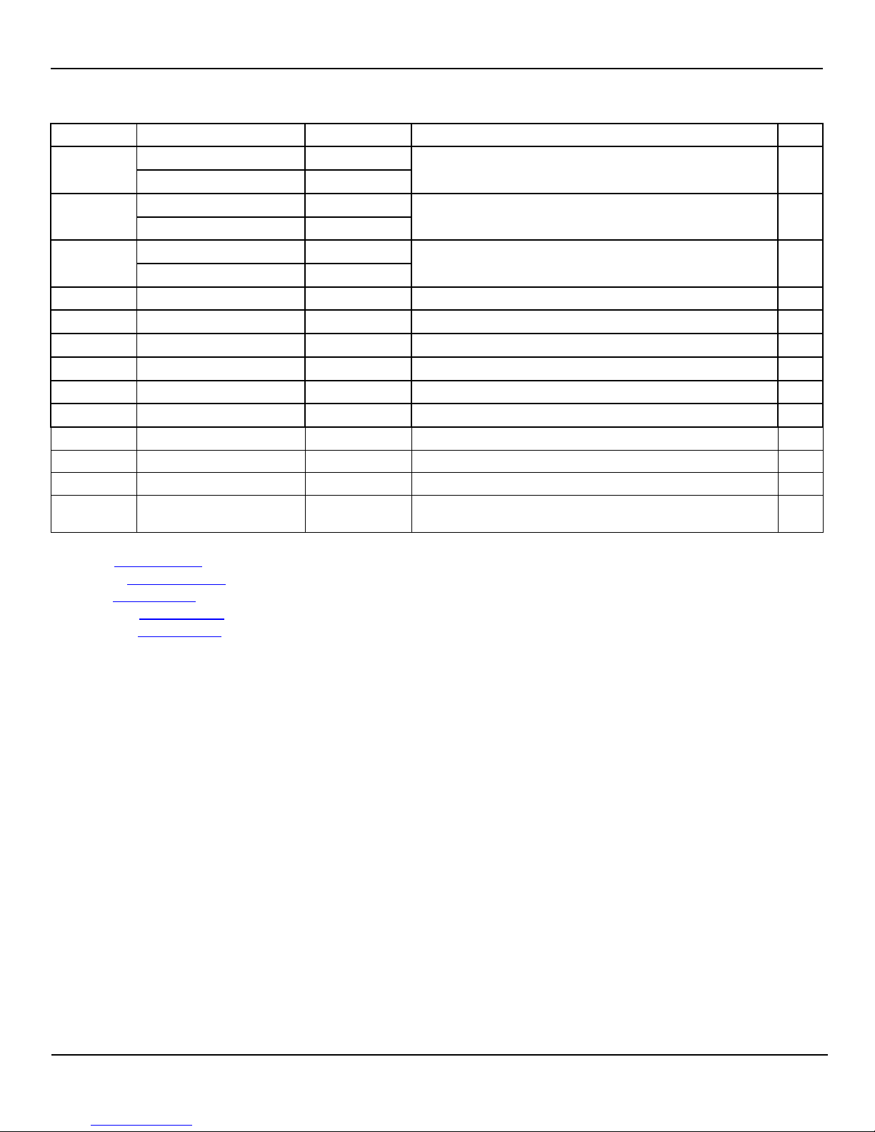
Bill of Materials
Item Part Number Manufacturer Description Qty.
C1, C5
GRM188R60J106ME47D Murata
CL10A106MQ8NNNC Samsung
GRM188R60J475ME19D Murata
C2, C3, C4
CL10A475MQ8NNNC Samsung
GRM31CR60J476ME19L Murata
C6
CL31A476MQHNNNE Samsung
D1 SML-LXT1206SRC Lumex
L1 IFSC1515AHER6R8M01 Vishay Dale
L2 CIG2MW4R7NNE Samsung 4.7µH, 1.1A Inductor, 140mΩ, 2.0mm × 1.6mm × 1.0mm 1
R1 RC1005F3833CS Samsung 383kΩ Resistor, 0402, 1% 1
R2 RC1005F1913CS Samsung 191kΩ Resistor, 0402, 1% 1
R3 RC1005F3923CS Samsung 392kΩ Resistor, 0402, 1% 1
R4 RC1005F5763CS Samsung 576kΩ Resistor, 0402, 1% 1
R5 RC1005F1003CS Samsung 100kΩ Resistor, 0402, 1% 1
R6 RC1005F80R6CS Samsung 80.6Ω Resistor, 0402, 1% 1
U1 MIC23099YFT Micrel
Notes:
1. Murata: www.murata.com
2. Samsung: www.samsung.com.
3. Lumex: www.lumex.com.
4. Vishay Dale: www.vishay.com.
5. Micrel, Inc.: www.micrel.com.
.
(1)
10µF/6.3V, Ceramic Capacitor, X5R, 0603, ±20% 2
(2)
4.7µF/6.3V, Ceramic Capacitor, X5R, 0603, ±20% 3
47µF/6.3V, Ceramic Capacitor, X5R, 1206, ±20% 1
(3)
1.7V/20mA, LED, 660NM RED WTR CLR, 1206 1
(4)
6.8µH, 1.5A Inductor, 90mΩ, 3.8mm × 3.8mm × 1.8mm 1
(5)
Single AA/AAA Cell Step-Up/Step-Down Regulators with
Battery Monitoring
1
May 30, 2014 7
Revision 1.0
Page 8
Micrel, Inc.
MIC23099 Evaluation Board
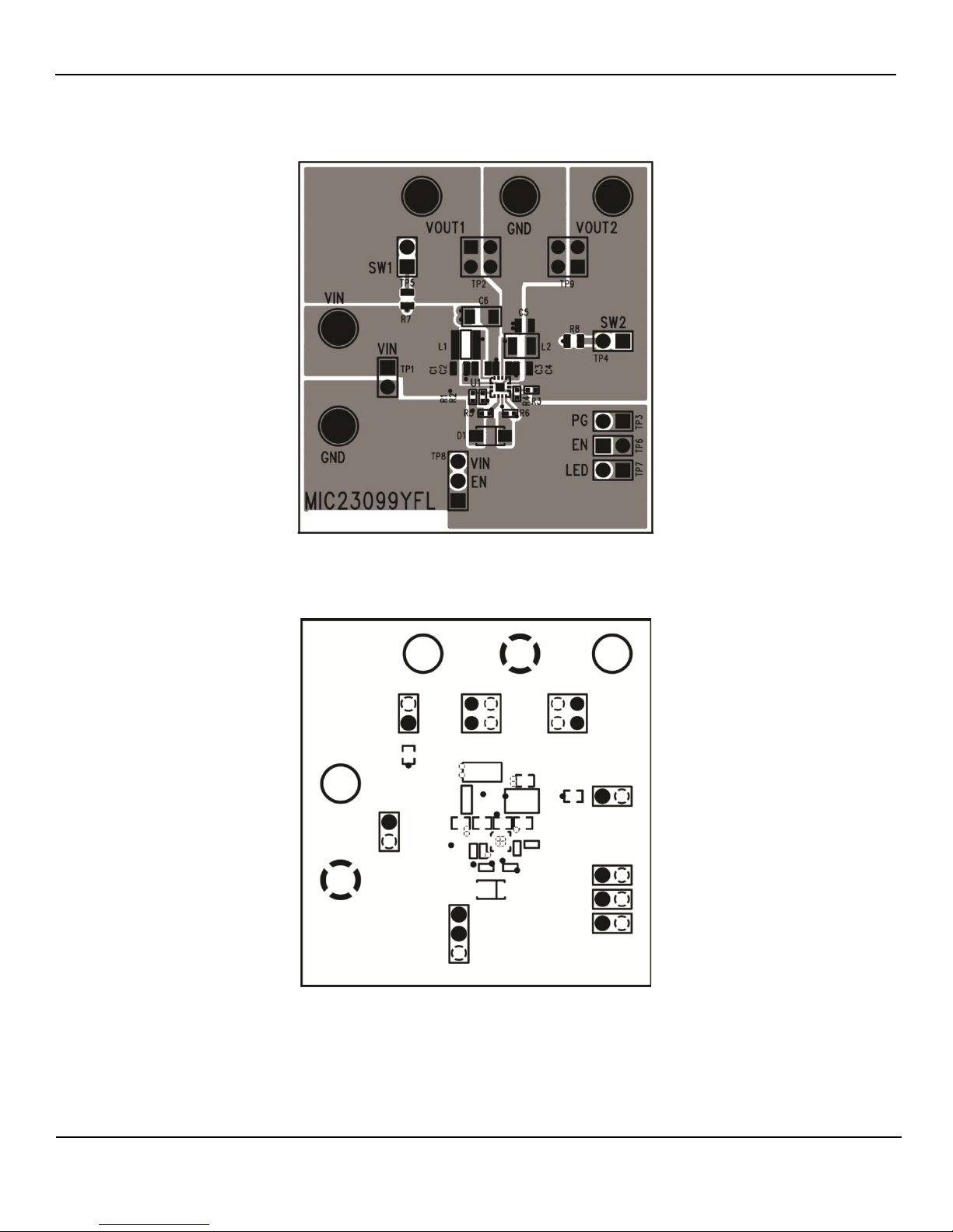
PCB Layout Recommendations
Top Layer (Power Trace Layer)
May 30, 2014 8
Layer 2 (Ground Plane)
Revision 1.0
Page 9
Micrel, Inc.
MIC23099 Evaluation Board
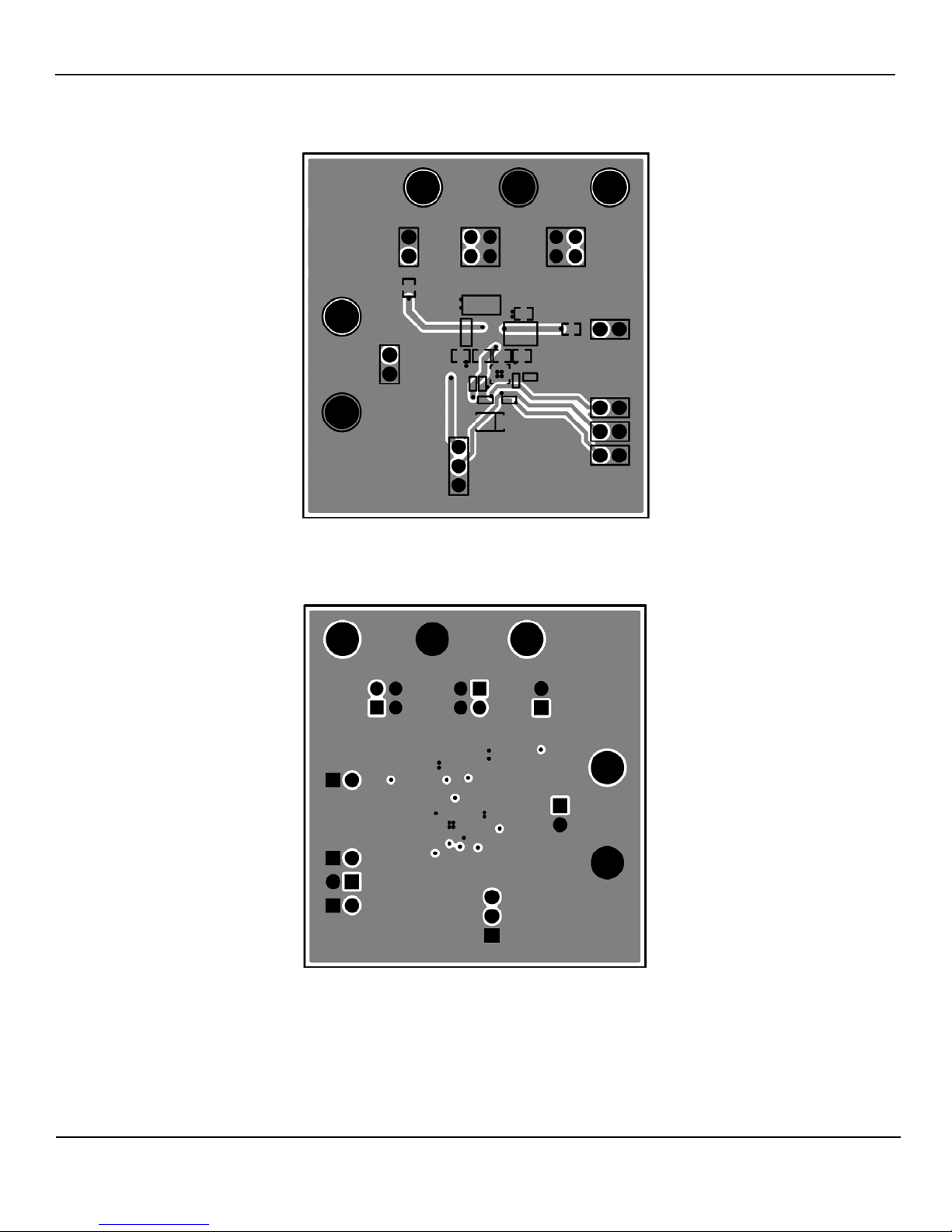
PCB Layout Recommendations (Continued)
Layer 3 (Routing Layer)
Bottom Layer (Ground Plane)
May 30, 2014 9
Revision 1.0
Page 10
Micrel, Inc.
MIC23099 Evaluation Board
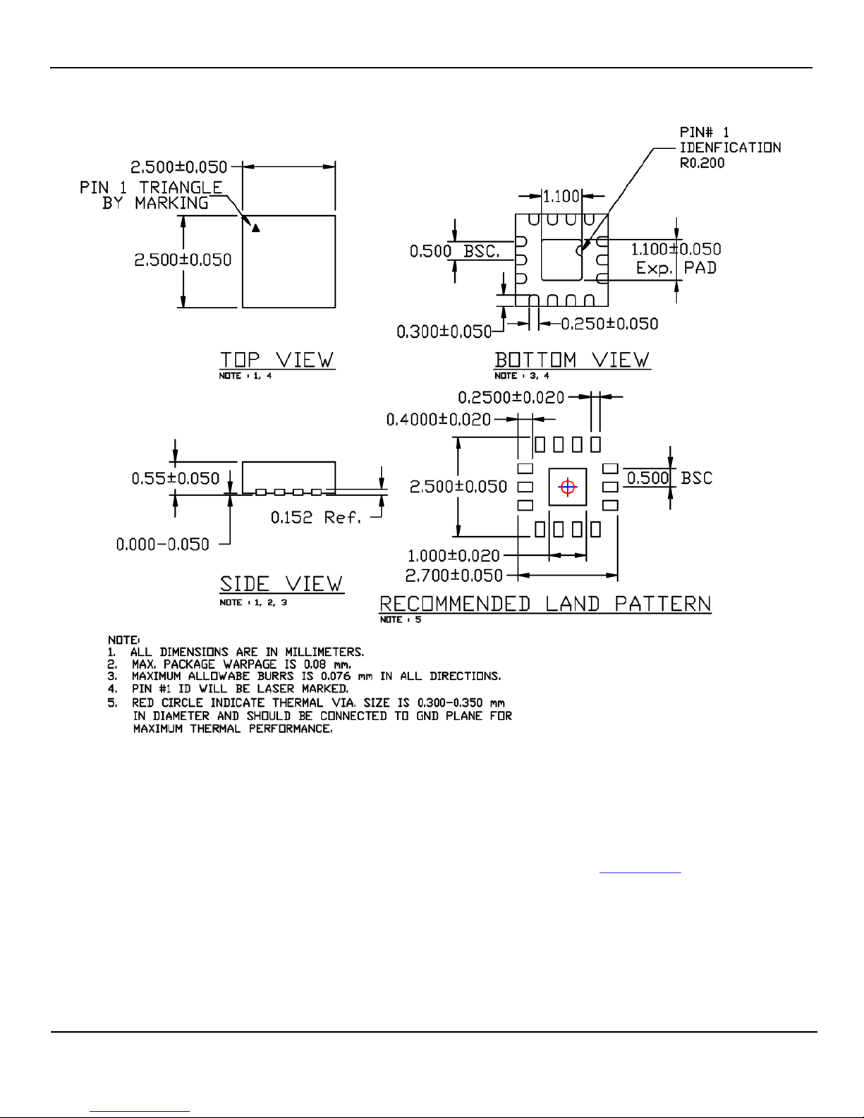
Package Information and Recommended Landing Pattern
(6)
Note:
6. Package information is correct as of the publication date. For updates and most current information, go to www.micrel.com
May 30, 2014 10
.
Revision 1.0
Page 11

Micrel, Inc.
MIC23099 Evaluation Board
MICREL, INC. 2180 FORTUNE DRIVE SAN JOSE, CA 95131 USA
nd whose failure to perform can be reasonably expected to result in a significant injury to the user. A
y
TEL +1 (408) 944-0800 FAX +1 (408) 474-1000 WEB http://www.micrel.com
Micrel makes no representations or warranties with respect to the accuracy or completeness of the information furnished in this data sheet. This
information is not intended as a warranty and Micrel does not assume responsibility for its use. Micrel reserves the right to change circuitry,
specifications and descriptions at any time without notice. No license, whether express, implied, arisi ng by estoppel or otherwise, t o any intellectual
property rights is granted by this document. Except as provided in Micrel’s terms and condit i ons of sale for such products, Micrel assum es no liabil ity
whatsoever, and Micrel disclaims any express or implied warranty relating to the sale and/or use of Micrel products including liability or warranties
relating to fitness for a particular purpose, merchantability, or infringement of any patent, copyright or other intel l ect ual property right.
Micrel Products are not designed or authorized for use as components in life support appliances, devices or systems where malfunction of a product
can reasonably be expected to result in personal injury. Life support devices or systems are devices or systems that (a) are intended for surgical
implant into the body or (b) support or sustain life, a
Purchaser’s use or sale of Micrel Products for use in life support appliances, devices or systems is a Purchaser’s own risk and Purchaser agrees to full
May 30, 2014 11
indemnify Micrel for any damages resulting from such use or sale.
© 2014 Micrel, Incorporated.
Revision 1.0
 Loading...