

查询MIC2205供应商
MIC2205
2MHz PWM Synchronous Buck
Regulator with LDO Standby Mode
General Description
The Micrel MIC2205 is a high efficiency 2MHz PWM
synchronous buck (step-down) regulator that
features a LOWQ™ LDO standby mode that draws
only 18µA of quiescent current. The MIC2205
allows an ultra-low noise, small size, and high
efficiency solution for portable power applications.
In PWM mode, the MIC2205 operates with a
constant frequency 2MHz PWM control. Under light
load conditions, such as in system sleep or standby
modes, the PWM switching operation can be
disabled to reduce switching losses. In this light
load LOWQ™ mode, the LDO maintains the output
voltage and draws only 18µA of quiescent current.
The LDO mode of operation saves battery life while
not introducing spurious noise and high ripple as
experienced with pulse skipping or bursting mode
regulators.
The MIC2205 operates from 2.7V to 5.5V input and
features internal power MOSFETs that can supply
up to 600mA output current in PWM mode. It can
operate with a maximum duty cycle of 100% for use
in low-dropout conditions.
The MIC2205 is available in the 3mm x 3mm MLF10L package with a junction operating range from
–40°C to +125°C.
Data sheets and support documentation can be
found on Micrel’s web site at www.micrel.com.
____________________________________________________________________________________________________
Features
• 2.7 to 5.5V supply voltage
• Light load LOWQ™ LDO mode
18µA quiescent current
Low noise, 75µVrms
• 2MHz PWM mode
Output current to 600mA
>95% efficiency
100% maximum duty cycle
• Adjustable output voltage option down to 1V
Fixed output voltage options available
• Ultra-fast transient response
• Stable with 1µF ceramic output capacitor
• Fully integrated MOSFET switches
• Micropower shutdown
• Thermal shutdown and current limit protection
• Pb-free 3mm x 3mm MLF-10L package
• –40°C to +125°C junction temperature range
Applications
• Cellular phones
• PDAs
• USB peripherals
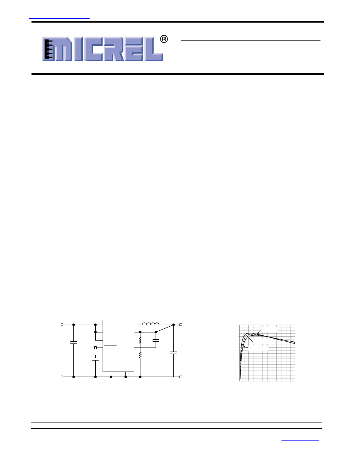
Typical Application
2.7V to 5.5V
V
GND
IN
C1
1µF
LowQ
C2
0.1µF
MIC2205
8
VIN
4
AVINSWLDO
6
EN
7
LOWQ
3
BIAS
PGND
AGND
10 1
FB
Adjustable Output Buck Regulator with LOWQ™ Mode
2.2µH
9
2
R1
100k
5
R2
125k
C3
100pF
V
C4
2.2µF
GND
OUT
1.8V
Efficiency
100
95
90
85
80
75
70
65
EFFICIENCY (%)
60
55
50
0 100 200 300 400 500 600
OUT
VIN=3V
VIN=3.6V
VIN=4.2V
OUTPUT CURRENT (mA)
Patent Pending
LOWQ is a trademark of Micrel, Inc
Micrel, Inc • 2180 Fortune Drive • San Jose, Ca 95131 • USA • tel +1 (408) 944-0800 • fax +1 (408) 474-1000 • http://www.micrel.com
April 2005
M9999-041105
www.micrel.com
Micrel, Inc. MIC2205
A
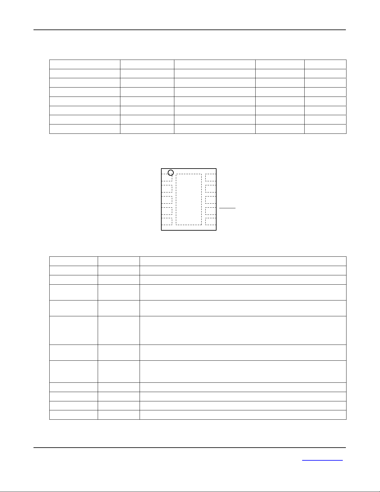
Ordering Information
Part Number Output Voltage
MIC2205-1.3YML 1.3V –40° to +125°C 3x3 MLF-10L Pb-free
MIC2205-1.38YML 1.38V –40° to +125°C 3x3 MLF-10L Pb-free
MIC2205-1.5YML 1.5V –40° to +125°C 3x3 MLF-10L Pb-free
MIC2205-1.58YML 1.58V –40° to +125°C 3x3 MLF-10L Pb-free
MIC2205-1.8YML 1.8V –40° to +125°C 3x3 MLF-10L Pb-free
MIC2205-1.85YML 1.85V –40° to +125°C 3x3 MLF-10L Pb-free
MIC2205YML Adj. –40° to +125°C 3x3 MLF-10L Pb-free
Note:
1. Other Voltage options available. Contact Micrel for details.
(1)
Junction Temp. Range Package Lead Finish
Pin Configuration
PGND
GND
LDO
BIAS
1
2
3
10
SW
9
VIN
8
Pin Description
Pin Number Pin Name Pin Function
1 AGND Analog (signal) Ground.
2 LDO LDO Output (Output): Connect to V
3 BIAS
4 AVIN
5 FB
6 EN
7
8 VIN Supply Voltage (Input): Supply voltage for the internal switches and drivers.
9 SW Switch (Output): Internal power MOSFET output switches.
10 PGND Power Ground.
EP GND Ground, backside pad.
_____
LOWQ
LOWQ
AVIN
4
FB EN
5
EP
7
6
3mm x 3mm MLF-10L (ML)
for LDO mode operation.
OUT
Internal circuit bias supply. Must be de-coupled to signal ground with a 0.1µF
capacitor and should not be loaded.
Analog Supply Voltage (Input): Supply voltage for the analog control circuitry and
LDO input power. Requires bypass capacitor to GND.
Feedback. Input to the error amplifier. For the Adjustable option, connect to the
external resistor divider network to set the output voltage. For fixed output
voltage options, connect to V
voltage.
Enable (Input). Logic low will shut down the device, reducing the quiescent
current to less than 5µA.
Enable LDO Mode (Input): Logic low enables the internal LDO and disables the
PWM operation. Logic high enables the PWM mode and disables the LDO
mode.
and an internal resistor network sets the output
OUT
April 2005
2
M9999-041105
www.micrel.com
Micrel, Inc. MIC2205
Absolute Maximum Ratings
(1)
Supply Voltage (VIN) ............................................ +6V
Output Switch Voltage (V
Output Switch Current (I
Logic Input Voltage (V
Storage Temperature (T
ESD Rating
(3)
....................................................... 3kV
Electrical Characteristics
) ............................... +6V
SW
)................................... 2A
SW
EN,VLOWQ
).............. -0.3V to VIN
)................ -60°C to +150°C
s
(4)
Operating Ratings
Supply Voltage (VIN)............................+2.7V to +5.5V
Logic Input Voltage (V
Junction Temperature (T
Junction Thermal Resistance
3x3 MLF-10L (θ
(2)
EN,VLOWQ
)...................................60°C/W
JA
) ..............-0.3V to VIN
)..............–40°C to +125°C
J
VIN = VEN = V
=3.6V; L = 2.2µH; C
LOWQ
= 2.2µF; TA = 25°C, unless noted. Bold values indicate –40°C< TJ < +125°C
OUT
Parameter Condition Min Typ Max Units
Supply Voltage Range
Under-Voltage Lockout
(turn-on) 2.45 2.55 2.65 V
2.7
5.5
V
Threshold
UVLO Hysteresis 100 mV
Quiescent Current, PWM
= 0.9 * V
V
FB
(not switching) 690
NOM
900
µA
mode
Quiescent Current, LDO
V
LOWQ
= 0V;I
= 0mA 16
OUT
29
µA
mode
Shutdown Current VEN = 0V 0.01
[Adjustable] Feedback
Voltage
± 1%
± 2% (over temperature)
[Fixed Output] Voltages Nominal V
tolerance
OUT
0.99
0.98
-1
-2
1
5
1.01
1.02
+1
+2
µA
V
%
FB pin input current 1 nA
Current Limit in PWM Mode VFB = 0.9 * V
Output Voltage Line
Regulation
Output Voltage Load
V
> 2V; VIN = V
OUT
< 2V; VIN = 2.7V to 5.5V; I
V
OUT
20mA < I
LOAD
NOM
+300mV to 5.5V; I
OUT
LOAD
LOAD
= 100mA
= 100mA
0.75
0.13 %
< 300mA 0.2
1
1.85
0.5
A
%
Regulation, PWM Mode
Output Voltage Load
Regulation, LDO Mode
Maximum Duty Cycle
PWM Switch ONResistance
100µA < I
V
LOWQ
V
≤ 0.4V
FB
LOAD
= 0V
< 50mA
ISW = 50mA VFB = 0.7V
= -50mA VFB = 1.1V
I
SW
(High Side Switch)
FB_NOM
FB_NOM
Oscillator Frequency
(Low Side Switch)
0.1
100
%
0.4
0.4
1.8
2
0.2
2.2
%
Ω
MHz
LOWQ threshold voltage
0.5
0.85
LOWQ Input Current 0.1
Enable Threshold
0.5
0.85
Enable Input Current 0.1
I
LDO Dropout Voltage
April 2005
= 50mA Note 5
OUT
110
3
1.3
2
1.3
2
V
µA
V
µA
mV
M9999-041105
www.micrel.com
Micrel, Inc. MIC2205
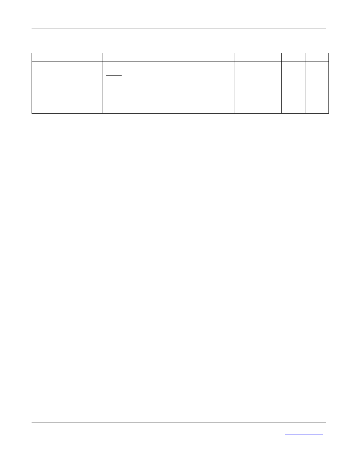
Parameter Condition Min Typ Max Units
60
75
120
Output Voltage Noise
LDO Current Limit LOWQ = 0V; V
Over-Temperature
Shutdown
Over-Temperature
Hysteresis
Notes
1. Exceeding the absolute maximum rating may damage the device.
2. The device is not guaranteed to function outside its operating rating.
3. Devices are ESD sensitive. Handling precautions recommended. Human body model: 1.5kΩ in series with 100pF.
4. Specification for packaged product only.
5. Dropout voltage is defined as the input-to-output differential at which the output voltage drops 2% below its nominal value that is
initially measured at a 1V differential. For outputs below 2.7V, the dropout voltage is the input-to-output voltage differential with a
minimum input voltage of 2.7V.
LOWQ = 0V; C
160
20
= 2.2μF, 10Hz to 100kHz
OUT
= 0V (LDO Mode)
OUT
µVrms
mA
°C
°C
April 2005
4
M9999-041105
www.micrel.com
Micrel, Inc. MIC2205
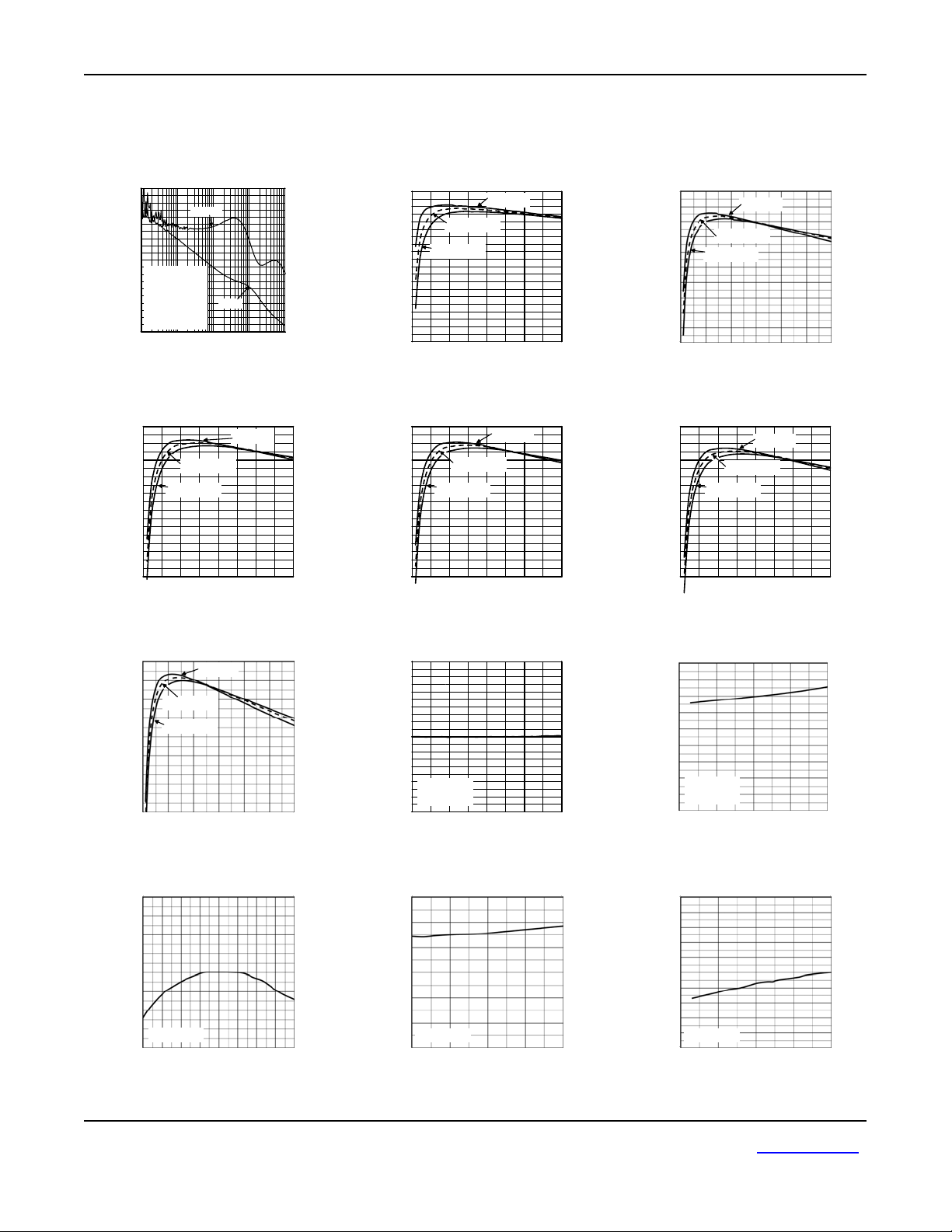
Typical Characteristics – PWM Mode
80
70
60
50
40
30
20
GAIN (dB)
10
0
-10
-20
1E+2 1E+3 1E+4 1E+5 1E+6
100
95
90
85
80
75
70
65
EFFICIENCY (%)
60
55
50
Bode Plot
Phase
VIN=3.6V
=1.8V
V
OUT
L=2.2 H
C
=2.2 F
OUT
= 120pF
C
FF
1k
FREQUENCY (Hz)
1.5V
VIN=4.2V
0 100 200 300 400
OUTPUT CURRENT (mA)
10k
Efficiency
OUT
VIN=3.6V
Gain
100k
VIN=3V
1M
144
126
108
90
72
54
36
18
0
-18
-36
PHASE (°)
2.5V
Efficiency
100
95
90
85
80
75
70
65
EFFICIENCY (%)
60
55
50
0 100 200 300 400
95
90
85
80
75
70
65
EFFICIENCY (%)
60
55
50
0 100 200 300 400
OUT
VIN=3V
VIN=3.6V
VIN=4.2V
OUTPUT CURRENT (mA)
1.38V
VIN=4.2V
OUTPUT CURRENT (mA)
Efficiency
OUT
VIN=3.6V
VIN=3V
1.8V
Efficiency
100
95
90
85
80
75
70
65
EFFICIENCY (%)
60
55
50
0 100 200 300 400 500 600
95
90
85
80
75
70
65
EFFICIENCY (%)
60
55
50
0 100 200 300 400
OUT
VIN=3V
VIN=3.6V
VIN=4.2V
OUTPUT CURRENT (mA)
1.2V
Efficiency
OUT
VIN=3V
VIN=3.6V
VIN=4.2V
OUTPUT CURRENT (mA)
1.0V
Efficiency
90
85
80
75
70
65
EFFICIENCY (%)
60
55
50
0 100 200 300 400 500 600
2.2
2.15
2.1
2.05
2
1.95
1.9
FREQUENCY (MHz)
1.85
1.8
-40 -20 0 20 40 60 80 100 120
OUT
VIN=3V
VIN=3.6V
VIN=4.2V
OUTPUT CURRENT (mA)
Frequency
vs. Temperature
VIN=3.6V
TEMPERATURE (°C)
1.010
1.008
1.006
1.004
1.002
1.000
0.998
0.996
0.994
FEEDBACK VOLTAGE (V)
0.992
0.990
1200
1000
CURRENT LIMIT (mA)
Load Regulation
VIN=3.6V
LowQ = V
IN
0 100 200 300 400
OUTPUT CURRENT (mA)
Peak Current Limit
vs. Supply Voltage
800
600
400
200
LowQ = V
0
2.7 3.4 4.1 4.8 5.5
IN
SUPPLY VOLTAGE (V)
Quiescent Current
vs. Supply Voltage
900
800
700
600
500
400
300
200
VIN=3.6V
100
V
QUIESCENT CURRENT (µA)
ENABLE THRESHOLD (V)
=0.9V
FB
0
2.7 3.4 4.1 4.8 5.5
SUPPLY VOLTAGE (V)
Enable Threshold
vs. Supply Voltage
1.5
1.4
1.3
1.2
1.1
1.0
0.9
0.8
0.7
0.6
LowQ = V
0.5
2.7 3.4 4.1 4.8 5.5
IN
SUPPLY VOLTAGE (V)
April 2005
5
M9999-041105
www.micrel.com

Micrel, Inc. MIC2205
Typical Characteristics – PWM Mode (cont.)
Turn-On Time
vs. Supply Voltage
100
90
80
70
60
50
40
30
20
TURN-ON DELAY (µs)
10
VIN=3.6V
0
2.7 3.4 4.1 4.8 5.5
SUPPLY VOLTAGE (V)
April 2005
6
M9999-041105
www.micrel.com

Micrel, Inc. MIC2205
Typical Characteristics - LDO Mode
PSRR
vs. Input Voltage
80
60
40
PSRR (dB)
I
20
OUT
V
OUT
C
OUT
0
1E-2 1E-1 1E+0 1E+1 1E+2 1E+3
0.01
0.1
vs. Supply Voltage
140
120
100
80
60
40
CURRENT LIMIT (mA)
20
0
2.7 3.4 4.1 4.8 5.5
SUPPLY VOLTAGE (V)
4.2V
=50mA
=1.8V
3.6V
=2.2 F
1
FREQUENCY (Hz)
10
Current Limit
LowQ = 0V
3V
100
PSRR
vs. Output Current
80
60
1k
40
PSRR (dB)
20
0
1E-2 1E-1 1E+0 1E+1 1E+2 1E+3
0.01
160
140
120
100
80
60
40
20
DROPOUT VOLTAGE (mV)
0
-40 -20 0 20 40 60 80 100120
I
OUT
VIN=3.6
V
=1.8V
OUT
=2.2 F
C
OUT
0.1
FREQUENCY (Hz)
Dropout Voltage
vs. Temperature
TEMPERATURE (°C)
=100 A
I
1
I
OUT
=50mA
OUT
10
V
OUT
I
= 50mA
OUT
LowQ = 0V
=0A
100
= 3.3V
1k
250
200
150
100
50
DROPOUT VOLTAGE (mV)
0
0 20406080100
80
70
60
50
40
30
20
10
DROPOUT VOLTAGE (mV)
0
-40 -20 0 20 40 60 80 100120
Dropout
vs. Output Current
V
=3.3V
OUT
OUTPUT CURRENT (mA)
Dropout Voltage
vs. Temperature
V
= 3.3V
OUT
I
= 25mA
OUT
LowQ = 0V
TEMPERATURE (°C)
Dropout Voltage
vs. Temperature
40
35
30
25
20
15
10
5
DROPOUT VOLTAGE (mV)
0
-40 -20 0 20 40 60 80 100120
TEMPERATURE (°C)
Enable Threshold Voltage
vs. Supply Voltage
1.5
1.4
1.3
1.2
1.1
1.0
0.9
0.8
0.7
ENABLE THRESHOLD (V)
0.6
0.5
2.7 3.4 4.1 4.8 5.5
SUPPLY VOLTAGE (V)
V
= 3.3V
OUT
I
= 10mA
OUT
LowQ = 0V
LowQ = 0V
Dropout Voltage
vs. Temperature
9
8
7
6
5
4
3
2
1
DROPOUT VOLTAGE (mV)
0
-40 -20 0 20 40 60 80 100120
TEMPERATURE (°C)
Turn-On Time
vs. Supply Voltage
100
90
80
70
60
50
40
30
20
TURN-ON DELAY (µs)
10
0
2.7 3.4 4.1 4.8 5.5
SUPPLY VOLTAGE (V)
V
OUT
I
= 1mA
OUT
LowQ = 0V
VIN=3.6V
LowQ = 0V
= 3.3V
1.836
1.827
1.818
1.809
1.800
1.791
1.782
OUTPUT VOLTAGE (V )
1.773
1.764
QUIESCENT CURRENT (µA)
Output Voltage
vs. Temperature
LowQ = 0V
-40 -20 0 20 40 60 80 100120
TEMPERATURE (°C)
Quiescent Current
vs. Temperature
25
I
=50mA
OUT
20
15
I
=100 A
OUT
10
5
0
-40 -20 0 20 40 60 80 100120
TEMPERATURE (°C)
I
=1mA
OUT
VIN=3.6V
LowQ = 0V
April 2005
7
M9999-041105
www.micrel.com

Micrel, Inc. MIC2205
Typical Characteristics – LDO Mode (cont.)
Quiescent Current
vs. Temperature
25
I
=100 A
OUT
20
15
10
5
QUIESCENT CURRENT (µA)
0
012345
SUPPLY VOLTAGE (V)
Output Voltage
vs. Output Current
1.836
1.827
1.818
1.809
1.8
1.791
1.782
OUTPUT VOLTAGE (V)
1.773
1.764
0 20406080100
OUTPUT CURRENT (mA)
I
=60mA
OUT
I
LowQ = 0V
VIN=3.6V
V
OUT
LowQ = 0V
OUT
=0A
=1.8V
Quiescent Current
vs. Supply Voltage
25
24
23
22
21
20
19
18
17
16
QUIESCENT CURRENT (µA)
15
2.7 3.4 4.1 4.8 5.5
SUPPLY VOLTAGE (V)
I
=100 A
OUT
LowQ = 0V
Quiescent Current
vs. Output Current
25
24
23
22
21
20
19
18
17
16
QUIESCENT CURRENT (µA)
15
0 20406080100
OUTPUT CURRENT (mA)
VIN=3.6V
LowQ = 0V
April 2005
8
M9999-041105
www.micrel.com

Micrel, Inc. MIC2205
Functional Diagram
VIN
AVIN
BIAS
EN
LOWQ
6
Enable and
Control Logic
Bias,
UVLO,
Thermal
Shutdown
LDO Block
LDO
Current
Limit
PWM
Control
Current Limit
HSD
Anti-Shoot
Through
LSD
N-Channel
Current Limit
Soft
Start
P-Channel
EA
1.0V
EA
1.0V
SW
FB
LDO
R1
R2
V
OUT
C
OUT
SGND
PGND
MIC2205 Block Diagram
April 2005
9
M9999-041105
www.micrel.com

Micrel, Inc. MIC2205
Functional Characteristics
Load Transient PWM Mode
LowQ = V
IN
(100mA/div)
Output Current
(50mV/div)
AC Coupled
Output Voltage
ENABLE
OUT
V
Time 20 s/div
Enable Transient PWM Mode
LowQ = 0V
(1V/div)
(50mV/div)
Time 40
s/div
April 2005
10
M9999-041105
www.micrel.com

Micrel, Inc. MIC2205
Functional Characteristics
April 2005
11
M9999-041105
www.micrel.com

Micrel, Inc. MIC2205
⎛
⎞ ⎠ ⎟
Functional Description
VIN
VIN provides power to the MOSFETs for the switch
mode regulator section, along with the current
limiting sensing. Due to the high switching speeds, a
1µF capacitor is recommended close to VIN and the
power ground (PGND) pin for bypassing. Please
refer to layout recommendations.
AVIN
Analog V
section and the bias through an internal 6 Ohm
resistor. AVIN and VIN must be tied together.
Careful layout should be considered to ensure high
frequency switching noise caused by VIN is reduced
before reaching AVIN.
LDO
The LDO pin is the output of the linear regulator and
should be connected to the output. In LOWQ mode
(LOWQ<1.5V), the LDO provides the output voltage.
In PWM mode (LOWQ>1.5V) the LDO pin is high
impedance.
EN
The enable pin provides a logic level control of the
output. In the off state, supply current of the device
is greatly reduced (typically <1µA). Also, in the off
state, the output drive is placed in a "tri-stated"
condition, where both the high side P-channel
Mosfet and the low-side N-channel are in an “off” or
non-conducting state. Do not drive the enable pin
above the supply voltage.
LOWQ
The LOWQ pin provides a logic level control
between the internal PWM mode and the low noise
linear regulator mode. With LOWQ pulled low
(<0.5V), quiescent current of the device is greatly
reduced by switching to a low noise linear regulator
mode that has a typical I
mode the output can deliver 60mA of current to the
output. By placing LOWQ high (>1.5V), this
transitions the device into a constant frequency
PWM buck regulator mode. This allows the device
the ability to efficiently deliver up to 600mA of output
current at the same output voltage.
BIAS
The BIAS pin supplies the power to the internal
power to the control and reference circuitry. The bias
is powered from AVIN through an internal 6Ω
resistor. A small 0.1µF capacitor is recommended
April 2005
(AVIN) provides power to the LDO
IN
of 18µA. In linear (LDO)
Q
for bypassing.
FB
The feedback pin (FB) provides the control path to
control the output. For adjustable versions, a resistor
divider connecting the feedback to the output is used
to adjust the desired output voltage. The output
voltage is calculated as follows:
R1
V
= V
OUT
where V
×
⎜
REF
⎝
is equal to 1.0V.
REF
R2
+1
A feedforward capacitor is recommended for most
designs using the adjustable output voltage option.
To reduce battery current draw, a 100K feedback
resistor is recommended from the output to the FB
pin (R1). Also, a feedforward capacitor should be
connected between the output and feedback (across
R1). The large resistor value and the parasitic
capacitance of the FB pin can cause a high
frequency pole that can reduce the overall system
phase margin. By placing a feedforward capacitor,
these effects can be significantly reduced.
Feedforward capacitance (C
) can be calculated as
FF
follows:
C
=
FF
1
160kHzR12
××
π
For fixed options A feed forward capacitor from the
output to the FB pin is required. Typically a 100pF
small ceramic capacitor is recommended
SW
The switch (SW) pin connects directly to the inductor
and provides the switching current nessasary to
operate in PWM mode. Due to the high speed
switching on this pin, the switch node should be
routed away from sensitive nodes.
PGND
Power ground (PGND) is the ground path for the
high current PWM mode. The current loop for the
power ground should be as small as possible and
separate from the Analog ground (AGND) loop.
Refer to the layout considerations for more details.
SGND
Signal ground (SGND) is the ground path for the
biasing and control circuitry. The current loop for the
signal ground should be separate from the Power
ground (PGND) loop. Refer to the layout
considerations for more details.
12
M9999-041105
www.micrel.com

Micrel, Inc. MIC2205
Applications Information
The MIC2205 is a 600mA PWM power supply that
utilizes a LOWQ™ light load mode to maximize
battery efficiency in light load conditions. This is
achieved with a LOWQ control pin that when pulled
low, shuts down all the biasing and drive current for
the PWM regulator, drawing only 18µA of operating
current. This allows the output to be regulated
through the LDO output, capable of providing 60mA
of output current. This method has the advantage of
producing a clean, low current, ultra low noise output
in LOWQ™ mode. During LOWQ™ mode, the SW
node becomes high impedance, blocking current
flow. Other methods of reducing quiescent current,
such as pulse frequency modulation (PFM) or
bursting techniques, create large amplitude, low
frequency ripple voltages that can be detrimental to
system operation.
When more than 60mA is required, the LOWQ pin
can be forced high, causing the MIC2205 to enter
PWM mode. In this case, the LDO output makes a
"hand-off" to the PWM regulator with virtually no
variation in output voltage. The LDO output then
turns off allowing up to 600mA of current to be
efficiently supplied through the PWM output to the
load.
Input Capacitor
A minimum 1µF ceramic is recommended on the
VIN pin for bypassing. X5R or X7R dielectrics are
recommended for the input capacitor. Y5V
dielectrics lose most of their capacitance over
temperature and are therefore, not recommended.
A minimum 1µF is recommended close to the VIN
and PGND pins for high frequency filtering. Smaller
case size capacitors are recommended due to their
lower ESR and ESL. Please refer to layout
recommendations for proper layout of the input
capacitor.
Output Capacitor
Even though the MIC2205 is optimized for a 2.2µF
output capacitor, output capacitance can be varied
from 1µF to 4.7µF. The MIC2205 utilizes type III
internal compensation and utilizes an internal high
frequency zero to compensate for the double pole
roll off of the LC filter. For this reason, larger output
capacitors can create instabilities. X5R or X7R
dielectrics are recommended for the output
capacitor. Y5V dielectrics lose most of their
capacitance over temperature and are therefore, not
recommended.
In addition to a 2.2µF, a small 10nF is recommended
close to the load for high frequency filtering. Smaller
case size capacitors are recommended due to there
lower ESR and ESL.
Inductor Selection
The MIC2205 is designed for use with a 2.2µH
inductor. Proper selection should ensure the
inductor can handle the maximum average and peak
currents required by the load. Maximum current
ratings of the inductor are generally given in two
methods; permissible DC current and saturation
current. Permissible DC current can be rated either
for a 40°C temperature rise or a 10% to 20% loss in
inductance. Ensure that the inductor selected can
handle the maximum operating current. When
saturation current is specified, make sure that there
is enough margin that the peak current will not
saturate the inductor. Peak inductor current can be
calculated as follows:
⎛
⎜
1V
OUT
⎜
⎝
+=
II
OUTPK
⎞
V
OUT
⎟
−
⎟
V
IN
⎠
Lf2
××
April 2005
13
M9999-041105
www.micrel.com

Micrel, Inc. MIC2205
Layout Recommendations
V
OUT
GND
V
IN
BIAS
C
L1
Note:
C
R1
BIAS
C
C
R1
MIC2205
FF
R2
Top
L
1
MIC2205
FF
R2
Bottom
LowQ
EN
V
OUT
GND
V
IN
LowQ
EN
The above figures demonstrate the recommended layout for the MIC2205 adjustable option.
April 2005
14
M9999-041105
www.micrel.com

Micrel, Inc. MIC2205
2.7V to 5.5V
2.7V to 5.5V
V
GND
V
GND
MIC2205
C2
8
VIN
4
AVINSWLDO
6
EN
7
LOWQ
3
BIAS
PGND
AGND
10 1
FB
IN
C1
1µF
LowQ
0.1µF
Adjustable Output
MIC2205
C2
8
VIN
4
AVINSWLDO
6
EN
7
LOWQ
3
BIAS
PGND
AGND
10 1
FB
IN
C1
1µF
LowQ
0.1µF
Fixed Output
2.2µH
9
2
2.2µH
C3
100pF
C3
100pF
R1
100k
5
R2
125k
9
2
5
V
C4
2.2µF
GND
V
C4
2.2µF
GND
OUT
OUT
Item Part Number Description Manufacturer Qty
C1
06036D105MAT2
GRM185R60J105KE21D
C4
06036D225MAT2
GRM188R61A225KE34
C3 VJ0402A101KXAA 100pF Ceramic Capacitor Vishay
C2
0201ZD103MAT2
GRM033R10J103KA01D
L1
LQH32CN2R2M53K
CDRH2D14-2R2
(1)
R1
CRCW04021002F 100kΩ 1% 0402 Vishay Dale
(1)
R2
CRCW04026652F
CRCW04021243F
CRCW04022003F
CRCW04024023F
U1
Notes:
1. For adjustable version only.
2. Sumida Tel: 408-982-9660
3. Murata Tel: 949-916-4000
4. Vishay Tel: 402-644-4218
5. Micrel, Inc. Tel: 408-944-0800
MIC2205BML
1µF Ceramic Capacitor X5R, 6.3V 0603
1µF Ceramic Capacitor X5R, 6.3V 0603
2.2µF Ceramic Capacitor X5R, 10V 0603
2.2µuF Ceramic Capacitor X5R, 10V 0603
10nF Ceramic Capacitor 6.3V 0201
10nF Ceramic Capacitor 6.3V 0201
2.2µH Inductor 97mΩ 3.2mmx2.5mmx1.55mm
2.2µH Inductor 94mΩ 3.2mmx3.2mmx1.55mm
66.5 kΩ 1% 0402 For 2.5V
124 kΩ 1% 0402 For 1.8 V
200 kΩ 1% 0402 For 1.5 V
402 kΩ 1% 0402 For 1.2 V
Open For 1.0 V
OUT
OUT
OUT
OUT
OUT
2MHz Synchronous Buck Regulator with LOWQTM
Mode
AVX
(4)
Murata
AVX
Murata
AVX
Murata
Murata
Sumida
(4)
(3)
1
(4)
(4)
(2)
Vishay Dale
Vishay Dale
Vishay Dale
Vishay Dale
Vishay Dale
Micrel, Inc.
1
1
1
1
(3)
1
(3)
(3)
(3)
(3)
(3)
(5)
1
April 2005
15
M9999-041105
www.micrel.com

Micrel, Inc. MIC2205
Package Information
10-Lead MLF™ (ML)
MICREL, INC. 2180 FORTUNE DRIVE SAN JOSE, CA 95131 USA
TEL +1 (408) 944-0800 FAX +1 (408) 474-1000 WEB http:/www.micrel.com
The information furnished by Micrel in this data sheet is believed to be accurate and reliable. However, no responsibility is assumed by Micrel
Micrel Products are not designed or authorized for use as components in life support appliances, devices or systems where malfunction of a
product can reasonably be expected to result in personal injury. Life support devices or systems are devices or systems that (a) are intended
for its use. Micrel reserves the right to change circuitry and specifications at any time without notification to the customer.
for surgical implant into the body or (b) support or sustain life, and whose failure to perform can be reasonably expected to result in a
significant injury to the user. A Purchaser’s use or sale of Micrel Products for use in life support appliances, devices or systems is a
Purchaser’s own risk and Purchaser agrees to fully indemnify Micrel for any damages resulting from such use or sale.
© 2004 Micrel, Incorporated.
April 2005
16
M9999-041105
www.micrel.com
 Loading...