

Micrel MIC2194 User Manual

MIC2194 Micrel
查询MIC2194供应商
MIC2194
400kHz SO-8 Buck Control IC
Final Information
General Description
Micrel’s MIC2194 is a high efficiency PWM buck control IC
housed in the SO-8 package. Its 2.9V to 14V input voltage
range allows it to efficiently step down voltages in 3.3V, 5V,
and 12V systems as well as 1- or 2-cell Li Ion battery powered
applications. The flexible architecture of the MIC2194 allows
for it to be configured as a buck or a buck-boost converter.
The MIC2194 solution saves valuable board space. The
device is housed in the space-saving SO-8 package, whose
low pin-count minimizes external components. Its 400kHz
PWM operation allows a small inductor and small output
capacitors to be used. The MIC2194 can implement allceramic capacitor solutions.
The MIC2194 drives a high-side P-channel MOSFET. A low
output driver impedance of 2Ω allows the MIC2194 to drive
large external MOSFETs to generate a wide range of output
currents. The MIC2194 can achieve maximum duty cycles of
100%, which can be useful in low headroom applications.
The MIC2194 is available in an 8 pin SOIC package with a
junction temperature range of –40°C to +125°C.
Features
• 2.9V to 14V input voltage range
• 400kHz oscillator frequency
• PWM current mode control
• 2Ω output drivers
• 100% maximum duty cycle
• 0.5µA micro-power shutdown
• Programmable UVLO
• Front edge blanking
• Cycle-by-cycle current limiting
• Frequency foldback short circuit protection
• 8-lead SOIC package
Applications
• Point of load power supplies
• Negative voltage buck-boost power supplies
• Distributed power systems
• Base stations
• Wireless modems
• ADSL line cards
• Servers
• Step down conversion in 3.3V, 5V, 12V systems
• 1-and 2-cell Li Ion battery operated equipment
T ypical Application
+3.3V
10µF
16V
V
IN
1µF
12V
47µF
20V
(×2)
2.2nF
VIN
EN/
UVLO
VDD FB
2k
COMP
0.012Ω
MIC2194BM
CS
OUTP
GND
Si4431A
(×2)
5.2µH
B530
10k
3.32k
V
OUT
5V, 5A
220µF
10V
(×2)
Adjustable Output Buck Converter
V
IN
10µF
16V
1µF
4.99k
10nF
0.040Ω
MIC2194BM
VIN
EN/
UVLO
VDD FB
COMP
CS
OUTP
GND
Si9803
22µH
B530
3.01k
22nF
220µF
10V
(×2)
1k
V
OUT
–5V, 0.6A
Positive-to-Negative Buck-Boost Converter
Micrel, Inc. • 1849 Fortune Drive • San Jose, CA 95131 • USA • tel + 1 (408) 944-0800 • fax + 1 (408) 944-0970 • http://www.micrel.com
October 2002 1 MIC2194
MIC2194 Micrel
Ordering Information
Part Number Output Voltage Frequency Junction Temp. Range Package
MIC2194BM Adjustable 400KHz –40°C to +125°C 8-lead SOP
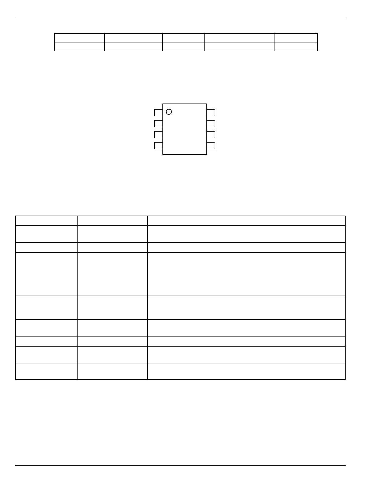
Pin Configuration
FB
EN/UVLO
CS
Pin Description
Pin Number Pin Name Pin Function
1 COMP Compensation (Output): Internal error amplifier output. Connect to a
2 FB Feedback (Input): The circuit regulates this pin to 1.245V.
3 EN/UVLO Enable/Undervoltage Lockout (Input): A low level on this pin will power down
4 CS The (–) input to the current limit comparator. A built-in offset of 110mV
5 VDD 3V internal linear-regulator output. VDD is also the supply voltage bus for the
6 GND Ground.
7 OUTP High current drive for the synchronous N-channel MOSFET. Voltage swing
8 VIN Input voltage to the circuit. Also the high side input to the current sense
1COMP
2
3
4
8 VIN
OUTP
7
GND
6
VDD
5
8 Lead SOIC (M)
capacitor or series RC network to compensate the regulator’s control loop.
the device, reducing the quiescent current to under 0.5µA. This pin has two
separate thresholds, below 1.5V the output switching is disabled, and below
0.9V the device is forced into a complete micropower shutdown. The 1.5V
threshold functions as an accurate undervoltage lockout (UVLO) with
hysteresis.
between VIN and CSL in conjunction with the current sense resistor sets the
current limit threshold level. This is also the (–) input to the current amplifier.
chip. Bypass to GND with 1µF.
is from ground to VIN. On-resistance is typically 3Ω @ 5VIN.
amplifier supplies power to the gate drive circuit.
MIC2194 2 October 2002
MIC2194 Micrel
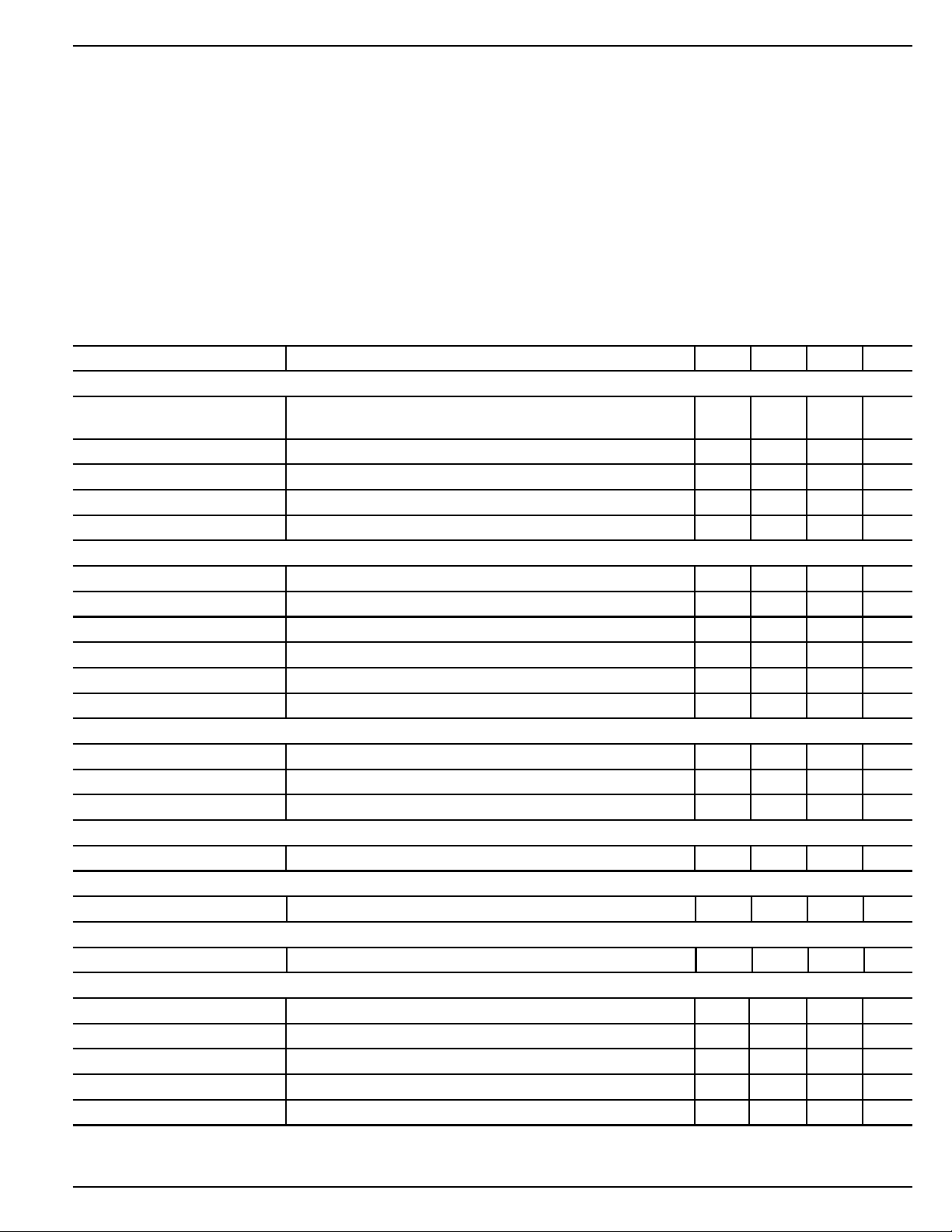
Absolute Maximum Ratings (Note 1)
Supply Voltage (V
Digital Supply Voltage (VDD) ...........................................7V
Enable Pin Voltage (VEN)............................. –0.3V to +15V
Comp Pin Voltage (V
) .....................................................15V
IN
)............................ –0.3V to +3V
COMP
Operating Ratings (Note 2)
Supply Voltage (V
Junction Temperature ....................... –40°C ≤ TJ ≤ +125°C
Package Thermal Resistance
θJA 8-lead SOP .................................................140°C/W
) .................................... +2.9V to +14V
IN
Feedback Pin Voltage (VFB) .......................... –0.3V to +3V
Current Sense Voltage (VIN –VCS)................. –0.3V to +1V
Power Dissipation (PD) ..................... 285mW @ TA = 85°C
Ambient Storage Temp ............................ –65°C to +150°C
ESD Rating, Note 3 ...................................................... 2kV
Electrical Characteristics
VIN = 5V, V
Parameter Condition Min Typ Max Units
Regulation
Feedback Voltage Reference (1%) 1.233 1.245 1.257 V
Feedback Bias Current 50 nA
Output Voltage Line Regulation 5V ≤ VIN ≤ 9V 0.15 % / V
Output Voltage Load Regulation 0mV < (VIN – VCS) < 75mV 0.9 %
Output Voltage Total Regulation 5V ≤VIN ≤ 9V, 0mV < (VIN – VCS) < 75mV (±3%) 1.208 1.282 V
Input & VDD Supply
VIN Input Current (IQ) (excluding external MOSFET gate current) 1 2 mA
Shutdown Current (ISD)V
Digital Supply Voltage (VDD)I
Digital Supply Load Regulation IL = 0 to 1mA 0.1 V
Undervoltage Lockout VDD upper threshold (turn on threshold) 2.65 V
UVLO Hysteresis 100 mV
Enable/UVLO
Enable Input Threshold 0.6 0.9 1.2 V
UVLO Threshold 1.4 1.5 1.6 V
Enable Input Current V
Current Limit
Current Limit Threshold Voltage VIN – VCS voltage to trip current limit 90 110 130 mV
Error Amplifier
Error Amplifier Gain 20 V/V
Current Amplifier
Current Amplifier Gain 3.0 V/V
Oscillator Section
Oscillator Frequency (fO) 360 400 440 kHz
Maximum Duty Cycle VFB = 1.0V 100 %
Minimum On Time VFB = 1.5V 165 ns
Frequency Foldback Threshold Measured on FB 0.3 V
Frequency Foldback Frequency 90 kHz
= 3.3V, TJ = 25°C, unless otherwise specified. Bold values indicate –40°C<TJ<+125°C.
OUT
(2%) 1.22 1.245 1.27 V
= 0V 0.5 5 µA
EN
= 0 2.82 3.0 3.18 V
L
EN/UVLO
= 5V 0.2 5 µA
October 2002 3 MIC2194
 Loading...