

Micrel MIC2184 User Manual
MIC2184 Micrel
查询MIC2184供应商
MIC2184
Low Voltage Buck PWM Control IC
Final Information
General Description
Micrel’s MIC2184 is a high efficiency PWM buck control IC.
With its wide input voltage range of 2.9V to 14V, the MIC2184
can be used to efficiently step voltages down in 1- or 2-cell Li
Ion battery powered applications, as well as in fixed 3.3V, 5V,
or 12V systems.
Efficiencies over 90% are achievable over a wide range of
load conditions with the MIC2184’s PWM control scheme.
The operating frequency can be divided by two by raising the
FREQ/2 pin to VDD. This allows the user to optimize efficiency
versus board space. It also allows the MIC2184 to be externally synchronized to frequencies below its nominal 400KHz.
The MIC2184 features an oscillator output, FreqOut, which
can be used to implement a simple charge pump in low
voltage applications. The output of the charge pump can be
fed into the gate drive power circuitry via the V
allowing enhanced gate drive, hence higher efficiencies,
despite low input voltages.
MIC2184 features a 1µA shutdown mode, and a programmable undervoltage lockout, making it well suited for portable
applications.
The MIC2184 is available in 16 pin SOP and QSOP package
options with a junction temperture range range from –40°C
to +125°C.
P pin,
IN
Features
• Input voltage range: 2.9V to 14V
• >90% efficiency
• Oscillator frequency of 400kHz
• Frequency divide-by-two pin
• Frequency sync to 600kHz
• FrequOut oscillator output allows simple charge pump
implementation in low voltage systems
• 1.245V reference output
• Front edge blanking
•5Ω output driver
• Soft start
• PWM current mode control
•1µA shutdown current
• Cycle-by-cycle current limiting
• Frequency foldback short circuit protection
• Adjustable under-voltage lockout
• 16 pin narrow-body SOIC and QSOP package options
Applications
• 3.3V to 2.5V/1.8V/1.5V conversion
• DC power distribution systems
• Wireless Modems
• ADSL line cards
• 1-and 2-cell Li Ion battery operated equipment
• Satellite Phones
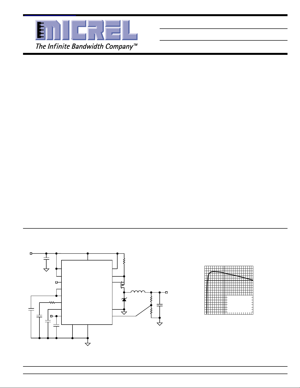
T ypical Application
= 3.3V
V
IN
120µF (x2)
6.3V
1
VINA
7
EN/UVLO
2
FreqOut
16
FREQ/2
10
VDD
4
COMP
3
SS
13
VREF
SYNC SGND
11 5
16
VINP
CSH
CSL
OUTP
MIC2184
PGND
FB
Adjustable Output Buck Converter
Micrel, Inc. • 1849 Fortune Drive • San Jose, CA 95131 • USA • tel + 1 (408) 944-0800 • fax + 1 (408) 944-0970 • http://www.micrel.com
December 10, 2001 1 MIC2184
9
8
14
12
6
15mΩ
Q3
Si9803DY(x2)
4.7µH
V
OUT
2.5V @5A
220µF(x2)
6.3V
MIC2184 EFFICIENCY
100
95
90
85
80
75
70
65
EFFICIENCY (%)
60
55
50
012345
OUTPUT CURRENT (A)
VIN = 3.3V
= 2.5V
V
OUT
= 200kHz
f
S
MIC2184 Micrel
Ordering Information
Part Number Output Voltage Frequency Junction Temp. Range Package
MIC2184BM Adjustable 400KHz –40°C to +125°C 16-lead SOP
MIC2184BQS Adjustable 400KHz –40°C to +125°C 16-lead QSOP
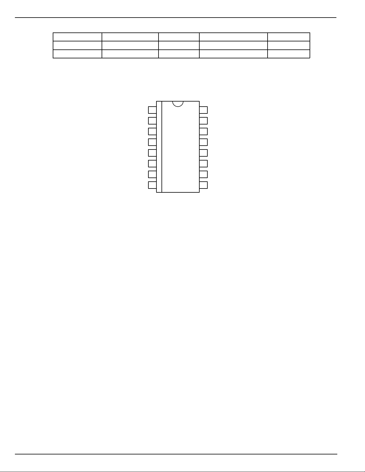
Pin Configuration
FreqOut
SS
COMP
SGND
FB
EN/UVLO
CSL
1VINA
2
3
4
5
6
7
8
16 Lead SOIC
(M)
16 VINP
FREQ/2
15
OUTP
14
VREF
13
PGND
12
SYNC
11
VDD
10
CSH
9
MIC2184 2 December 10, 2001
MIC2184 Micrel
Pin Description
Pin Number Pin Name Pin Function
1 VINA Analog voltage input voltage to the circuit. This powers up the analog
sections of the die and does not need to be the same voltage as Pin 16
(VINP).
2 FreqOut This provides a digital signal output signal at half the switching frequency.
This signal swings from 0 to 3V, and can be used to drive an external
capacitive doubler to provide a higher voltage to the VINP input.
3 SS Soft start reduces the inrush current and delays and slows the output voltage
rise time. A 5µA current source will charge the capacitor up to V
capacitor will soft start the switching regulator in 1.5ms.
4 COMP Compensation (Output): Internal error amplifier output. Connect to a
capacitor or series RC network to compensate the regulator’s control loop.
5 SGND Small signal ground: must be routed separately from other grounds to the (-)
terminal of C
6 FB Feedback Input - the circuit regulates this pin to 1.245V.
7 EN/UVLO Enable/UnderVoltage Lockout (input): A low level on this pin will power down
the device, reducing the quiescent current to under 5uA. This pin has two
separate thresholds, below 1.5V the output switching is disabled, and below
0.9V the part is forced into a complete micropower shutdown. The 1.5V
threshold functions as an accurate undervoltage lockout (UVLO) with 140mV
hysteresis.
8 CSL The (-) input to the current limit comparator. A built in offset of 100mV
between CSH and CSL in conjunction with the current sense resistor sets
the current limit threshold level. This is also the (-) input to the current
amplifier.
9 CSH The (+) input to the current limit comparator. A built in offset of 100mV
between CSH and CSL in conjunction with the current sense resistor sets
the current limit threshold level. This is also the (+) input to the current
amplifier.
10 VDD 3V internal linear-regulator output. VDD is also the supply voltage bus for the
chip. Bypass to SGND with 1µF.
11 SYNC Frequency Synchronization (Input): Connect an external clock signal to
synchronize the oscillator. Leading edge of signal above 1.5V starts the
switching cycle. Connect to SGND if not used.
12 PGND MOSFET driver power ground, connects to source of synchronous MOSFET
and the (-) terminal of CIN.
13 VREF The 1.245V voltage reference is available on this pin. A 0.1µF capacitor
should be connected from this pin to ground.
14 OUTP High current drive for high side P channel MOSFET. Voltage swing is from
ground to VINP. On-resistance is typically 2.5Ω.
15 FREQ/2 When this is low, the oscillator frequency is 400KHz. When this pin is raised
to VDD, the oscillator frequency is 200KHz.
16 VINP Power Input voltage to the circuit. The output gate drivers are powered from
this supply. The current sense resistor R
possible to this pin.
OUT
.
should be connected as close as
CS
. A 1µF
DD
December 10, 2001 3 MIC2184
MIC2184 Micrel
Absolute Maximum Ratings (Note 1)
Supply Voltage (V
Digital Supply Voltage (VDD) ...........................................7V
Comp Pin Voltage (V
Feedback Pin Voltage (VFB) .......................... –0.3V to +3V
Enable Pin Voltage (V
Current Sense Voltage (V
Sync Pin Voltage (V
Freq/2 Pin Voltage (V
A, VINP) .........................................15V
IN
)............................ –0.3V to +3V
COMP
EN/UVLO
SYNC
FREQ/2
) ..................... –0.3V to 15V
CSH–VCSL
) ............... –0.3V to 1V
) ................................ –0.3V to 7V
) ............................ -0.3V to 7V
Operating Ratings (Note 2)
Supply Voltage (V
Ambient Operating Temperature......... –40°C ≤ TA ≤ +85°C
Junction Temperature ....................... –40°C ≤ TJ ≤ +125°C
Output Voltage Range...................................... 1.3V to 12V
PackageThermal Resistance
θJA 16-lead SOP ...............................................100°C/W
θJA 16-lead QSOP.............................................163°C/W
A, VINP) ........................ +2.9V to +14V
IN
Power Dissipation (PD)
16 lead SOIC.................................400mW @ TA = 85°C
16 lead QSOP ...............................245mW @ TA = 80°C
Ambient Storage Temp ............................–65°C to +150°C
ESD Rating, ............................................................. Note 3
Electrical Characteristics
VINA = VINP = V
–40ºC < TJ < +125ºC.
Parameter Condition Min Typ Max Units
Regulation
Feedback Voltage Reference (±1%) 1.233 1.245 1.257 V
Feedback Bias Current 50 nA
Output Voltage Line Regulation 5V ≤ VIN ≤ 12V 0.04 % / V
Output Voltage Load Regulation 0mV < (V
Output Voltage Total Regulation 5V ≤ VINA ≤ 12V, 0mV < (V
Input & VDD Supply
VINA Input Current 0.7 mA
VINP Input Current, Note 4 (Excluding external MOSFET gate current) 1.0 mA
Shutdown Quiescent Current V
Digital Supply Voltage (VDD)I
Digital Supply load regulation IL = 0 to 1mA 0.03 V
Undervoltage Lockout VDD upper threshold (turn on threshold) 2.75 V
UVLO Hysteresis 100 mV
Reference Output(VREF)
Reference Voltage (±1.5%) 1.226 1.245 1.264 V
Reference Voltage Line 5V < VINA < 12V 2 mV
Regulation
Reference Voltage Load 0 < I
Regulation
Enable/UVLO
Enable Input Threshold 0.6 0.9 1.2 V
UVLO Threshold (Turn-on threshold) 1.4 1.5 1.6 V
UVLO Hysteresis 140 mV
Enable Input Current V
CSH
= 5V, V
= 3.3V, V
OUT
EN/UVLO
(±2%) 1.22 1.27 V
EN/UVLO
= 0 2.82 3.0 3.18 V
L
(±2.5%) 1.213 1.276 V
REF
EN/UVLO
= 5V, V
– V
CSH
= 0V; (I
< 100µA1mV
= 5V 0.2 5 µA
) < 75mV 0.9 %
CSL
VINA
= 0V, TJ = 25ºC, unless otherwise specified. Bold values indicate
FREQ/2
– V
CSH
+ I
) 0.5 5 µA
VINP
) < 75mV (±3%) 1.208 1.282 V
CSL
MIC2184 4 December 10, 2001
 Loading...