

MICREL MIC2182-5.0BSM, MIC2182BM, MIC2182BSM, MIC2182-5.0BM, MIC2182-3.3BM Datasheet
...
MIC2182 Micrel
MIC2182
High-Efficiency Synchronous Buck Controller
Final Information
General Description
Micrel’s MIC2182 is a synchronous buck (step-down) switching regulator controller. An all N-channel synchronous architecture and powerful output drivers allow up to a 20A output
current capabilty. The PWM and skip-mode control scheme
allows efficiency to exceed 95% over a wide range of load
current, making it ideal for battery powered applications, as
well as high current distributed power supplies.
The MIC2182 operates from a 4.5V to 32V input and can
operate with a maximum duty cycle of 86% for use in lowdropout conditions. It also features a shutdown mode that
reduces quiescent current to 0.1µA.
The MIC2182 achieves high efficiency over a wide output
current range by automatically switching between PWM and
skip mode. Skip-mode operation enables the converter to
maintain high efficiency at light loads by turning off circuitry
pertaining to PWM operation, reducing the no-load supply
current from 1.6mA to 600µA. The operating mode is internally selected according to the output load conditions. Skip
mode can be defeated by pulling the PWM pin low which
reduces noise and RF interference.
The MIC2182 is available in a 16-pin SOP (small-outline
package) and SSOP (shrink small-outline package) with an
operating range from –40°C to +85°C.
Features
• 4.5V to 32V Input voltage range
• 1.25V to 6V Output voltage range
• 95% efficiency
• 300kHz oscillator frequency
• Current sense blanking
• 5Ω impedance MOSFET Drivers
• Drives N-channel MOSFETs
• 600µA typical quiescent current (skip-mode)
• Logic controlled micropower shutdown (IQ < 0.1µA)
• Current-mode control
• Cycle-by-cycle current limiting
• Built-in undervoltage protection
• Adjustable undervoltage lockout
• Easily synchronizable
• Precision 1.245V reference output
• 0.6% total regulation
• 16-pin SOP and SSOP packages
• Frequency foldback overcurrent protection
• Sustained short-circuit protection at any input voltage
• 20A output current capability
Applications
• DC power distribution systems
• Notebook and subnotebook computers
• PDAs and mobile communicators
• Wireless modems
• Battery-operated equipment
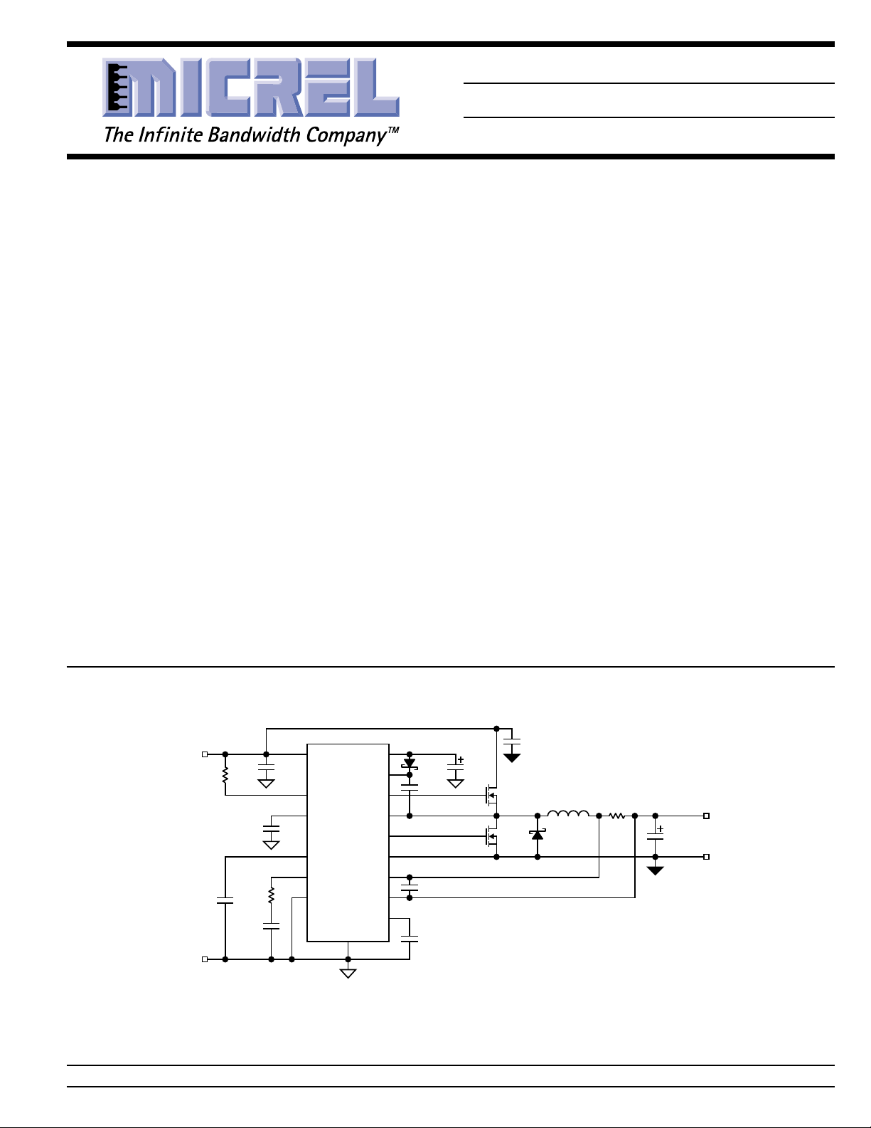
Typical Application
Q2*
Si4884
Q1*
Si4884
C11
22uf
35V
x2
10µH
D1
B140
L1
R2
0.02Ω
C7
220uf
10V ×2
V
OUT
3.3V/4A
GND
V
IN
4.5V to 30V*
GND
R7
100k
C3
0.1µF
2.2nF
C2
MIC2182-3.3BSM
10
VIN
C5
0.1µF
6
EN/UVLO
2
PWM
C4
1nF
1
SS
3
COMP
5
R1
SYNC
2k
SGND
4
VDD
BST
HSD
VSW
LSD
PGND
CSH
VOUT
VREF
D2
SD103BWS
11
14
C6
0.1µF
16
15
13
12
8
C13, 1nF
9
7
C1
0.1µF
C9
4.7µF
16V
* 30V maximum input voltage limit is due
to standard 30V MOSFET selection.
See “Application Information” section for
5V to 3.3V/10A and other circuits.
4.5V–30V* to 3.3V/4A Converter
Micrel, Inc. • 1849 Fortune Drive • San Jose, CA 95131 • USA • tel + 1 (408) 944-0800 • fax + 1 (408) 944-0970 • http://www.micrel.com
June 2000 1 MIC2182

MIC2182 Micrel
Ordering Information
Part Number Voltage Temperature Range Package
MIC2182BM Adjustable –40°C to +85°C 16-pin narrow SOP
MIC2182-3.3BM 3.3V –40°C to +85°C 16-pin narrow SOP
MIC2182-5.0BM 5.0V –40°C to +85°C 16-pin narrow SOP
MIC2182BSM Adjustable –40°C to +85°C 16-pin narrow SSOP
MIC2182-3.3BSM 3.3V –40°C to +85°C 16-pin narrow SSOP
MIC2182-5.0BSM 5.0V –40°C to +85°C 16-pin narrow SSOP
Pin Configuration
SS
1
MIC2182
16
HSD
SS
MIC2182-x.x
1
16
HSD
PWM
COMP
SGND
SYNC
EN/UVLO
FB
CSH
2
3
4
5
6
7
8
15
14
13
12
11
10
Adjustable
16-pin SOP (M)
16-Pin SSOP (SM)
9
VSW
BST
LSD
PGND
VDD
VIN
VOUT
PWM
COMP
SGND
SYNC
EN/UVLO
VREF
CSH
2
3
4
5
6
7
8
15
14
13
12
11
10
Fixed
16-pin SOP (M)
16-Pin SSOP (SM)
9
VSW
BST
LSD
PGND
VDD
VIN
VOUT
MIC2182 2 June 2000
MIC2182 Micrel
Pin Description
Pin Number Pin Name Pin Function
1 SS Soft-Start (External Component): Connect external capacitor to ground to
reduce inrush current by delaying and slowing the output voltage rise time.
Rise time is controlled by an internal 5µA current source that charges an
external capacitor to VDD.
2 PWM PWM/Skip-Mode Select (Input): Low sets PWM-mode operation. 1nF
capacitor to ground sets automatic PWM/skip-mode selection.
3 COMP Compensation (Output): Internal error amplifier output. Connect to capacitor
or series RC network to compensate the regulator control loop.
4 SGND Small Signal Ground (Return): Route separately from other ground traces to
the (–) terminal of C
5 SYNC Frequency Synchronization (Input): Optional. Connect to external clock
signal to synchronize the oscillator. Leading edge of signal above the
threshold terminates the switching cycle. Connect to SGND if unused.
6 EN/UVLO Enable/Undervoltage Lockout (Input): Low-level signal powers down the
controller. Input below the 2.5V threshold disables switching and functions
as an accurate undervoltage lockout (UVLO). Input below the threshold
forces complete micropower (< 0.1µA) shutdown.
7 (fixed) VREF Reference Voltage (Output): 1.245V output. Requires 0.1µf capacitor to
ground.
7 (adj) FB Feedback (Input): Regulates FB pin to 1.245V. See “Application Information”
for resistor divider calculations.
8 CSH Current-Sense High (Input): Current-limit comparator noninverting input. A
built-in offset of 100mV between CSH and V
current-sense resistor set the current-limit threshold level. This is also the
positive input to the current sense amplifier.
9 VOUT Current-Sense Low (Input): Output voltage feedback input and inverting
input for the current limit comparator and the current sense amplifier.
10 VIN [Battery] Unregulated Input (Input): +4.5V to +32V supply input.
11 VDD 5V Internal Linear-Regulator (Output): VDD is the external MOSFET gate
drive supply voltage and an internal supply bus for the IC. Bypass to SGND
with 4.7µF. VDD can supply up to 5mA for external loads.
12 PGND MOSFET Driver Power Ground (Return): Connects to source of synchro-
nous MOSFET and the (–) terminal of C
13 LSD Low-Side Drive (Output): High-current driver output for external synchronous
MOSFET. Voltage swing is between ground and VDD.
14 BST Boost (Input): Provides drive voltage for the high-side MOSFET driver. The
drive voltage is higher than the input voltage by VDD minus a diode drop.
15 VSW Switch (Return): High side MOSFET driver return.
16 HSD High-Side Drive (Output): High-current driver output for high-side MOSFET.
This node voltage swing is between ground and VIN + 5V – V
OUT
.
pins in conjunction with the
OUT
IN
diode drop
.
June 2000 3 MIC2182
MIC2182 Micrel
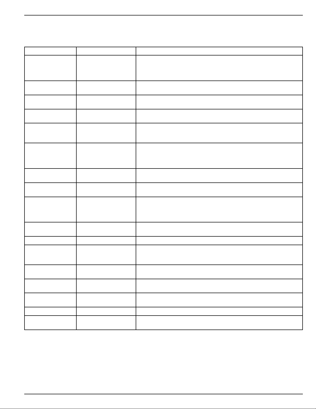
Absolute Maximum Ratings (Note 1)
Analog Supply Voltage (V
Digital Supply Voltage (VDD) .........................................+7V
Driver Supply Voltage (BST)....................................V
Sense Voltage (V
Sync Pin Voltage (V
OUT
SYNC
Enable Pin Voltage (V
) .......................................+34V
IN
+7V
IN
, CSH) ............................. 7V to –0.3V
) ................................ 7V to –0.3V
EN/UVLO
) ......................................V
Operating Ratings (Note 2)
Analog Supply Voltage (V
Ambient Temperature (TA).........................–40°C to +85°C
Junction Temperature (TJ) ....................... –40°C to +125°C
Package Thermal Resistance
SOP (θJA) ..........................................................100°C/W
IN
SSOP (θJA)........................................................150°C/W
) ........................ +4.5V to +32V
IN
Power Dissipation (PD)
SOP................................................400mW @ TA= 85°C
SSOP ............................................. 270mW @ TA= 85°C
Ambient Storage Temperature (TS) ......... –65°C to +150°C
ESD, Note 3
Electrical Characteristics
VIN = 15V; SS = open; V
noted
Parameter Condition Min Typ Max Units
MIC2182 [Adjustable], (Note 5)
Feedback Voltage Reference 1.233 1.245 1.257 V
Feedback Voltage Reference 1.220 1.245 1.270 V
Feedback Voltage Reference 4.5V < VIN < 32V, 0 < V
Feedback Bias Current 10 nA
Output Voltage Range 1.25 6 V
Output Voltage Line Regulation VIN = 4.5V to 32V, V
Output Voltage Load Regulation 25mV < (V
Output Voltage Total Regulation
MIC2182-3.3
Output Voltage 3.267 3.3 3.333 V
Output Voltage 3.234 3.3 3.366 V
Output Voltage 4.5V < VIN < 32V, 0 < V
Output Voltage Line Regulation VIN = 4.5V to 32V, V
Output Voltage Load Regulation 25mV < (V
Output Voltage Total Regulation
MIC2182-5.0
Output Voltage 4.95 5.0 5.05 V
Output Voltage 4.90 5.0 5.10 V
Output Voltage 6.5V < VIN < 32V, 0 < V
Output Voltage Line Regulation VIN = 6.5V to 32V, V
Output Voltage Load Regulation 25mV < (V
Output Voltage Total Regulation 0mV < (V
Input and VDD Supply
PWM Mode V
Skip Mode IL = 0mA, V
Shutdown Quiescent Current V
Digital Supply Voltage (VDD)I
Undervoltage Lockout VDD upper threshold (turn on threshold) 4.2 V
PWM
= 0V; V
= 5V; I
SHDN
0mV < (V
0mV < (V
PWM
EN/UVLO
= 0mA to 5mA 4.7 5.3 V
L
CSH
CSH
CSH
= 0V, excluding external MOSFET gate drive current 1.6 2.5 mA
= 0V 0.1 5 µA
= 0.1A; TA = 25°C, bold values indicate –40°C ≤ TA ≤ +85°C; Note 4; unless
LOAD
– V
CSH
– V
CSH
CSH
CSH
CSH
PWM
– V
– V
– V
– V
– V
– V
) < 75mV (PWM mode only) 0.5 %
OUT
) < 75mV (full load range) 4.5V < VIN < 32V
OUT
– V
CSH
– V
CSH
) < 75mV (PWM mode only) 0.5 %
OUT
) < 75mV (full load range) 4.5V < VIN < 32V
OUT
– V
CSH
– V
CSH
) < 75mV (PWM mode only) 0.5 %
OUT
) < 75mV (full load range)
OUT
floating (1nF capacitor to ground) 600 1500 µA
< 75mV 1.208 1.245 1.282 V
OUT
= 50mV 0.03 %/V
OUT
0.6 %
< 75mV 3.201 3.3 3.399 V
OUT
= 50mV 0.03 %/V
OUT
0.8 %
< 75mV 4.85 5.0 5.150 V
OUT
= 50mV 0.03 %/V
OUT
6.5V < VIN < 32V
0.8 %
VDD lower threshold (turn off threshold) 4.1 V
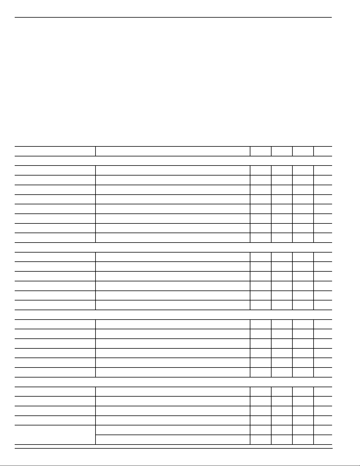
MIC2182 4 June 2000
MIC2182 Micrel
Parameter Condition Min Typ Max Units
Reference Output (Fixed Versions Only)
Reference Voltage 1.220 1.245 1.270 V
Reference Line Regulation 6V < VIN < 32V 1 mV
Reference Load Regulation 0µA < I
Enable/UVLO
Enable Input Threshold 0.6 1.1 1.6 V
UVLO Threshold 2.2 2.5 2.8 V
Enable Input Current V
EN/UVLO
Soft Start
Soft-Start Current VSS = 0V –3.5 –5 –6.5 µA
Current Limit
Current-Limit Threshold Voltage V
CSH
Error Amplifier
Error Sense Amplifier Gain 20
Current Amp
Current Sense Amplifier Gain 2.0
Oscillator Section
Oscillator Frequency 270 300 330 kHz
Maximum Duty Cycle 86 %
Minimum On-Time V
OUT
SYNC Threshold Level 0.7 1.3 1.9 V
SYNC Input Current V
SYNC
SYNC Minimum Pulse Width 200 ns
SYNC Capture Range Note 6 330 kHz
Frequency Foldback Threshold measured at VOUT pin 0.75 0.95 1.15 V
Foldback Frequency 60 kHz
Gate Drivers
Rise/Fall Time CL = 3000pF 60 ns
Output Driver Impedance source 5 8.5 Ω
sink 3.5 6 Ω
Driver Nonoverlap Time 80 ns
PWM Input
PWM Input Current V
Note 1. Exceeding the absolute maximum rating may damage the device.
Note 2. The device is not guaranteed to function outside its operating rating.
Note 3. Devices are ESD sensitive. Handling precautions recommended. Human body model, 1.5k in series with 100pF.
Note 4. 25°C limits are 100% production tested. Limits over the operating temperature range are guaranteed by design and are not production tested.
Note 5. VIN > 1.3 × V
Note 6. See applications information for limitations on the maximum operating frequency.
(for the feedback voltage reference and output voltage line and total regulation).
OUT
PWM
< 100µA2mV
REF
= 5V 0.1 5 µA
= V
OUT
= V
OUT(nominal)
+ 200mV 140 250 ns
75 100 135 mV
= 5V 0.1 5 µA
= 0V –10 µA
June 2000 5 MIC2182
MIC2182 Micrel
µ
(
)
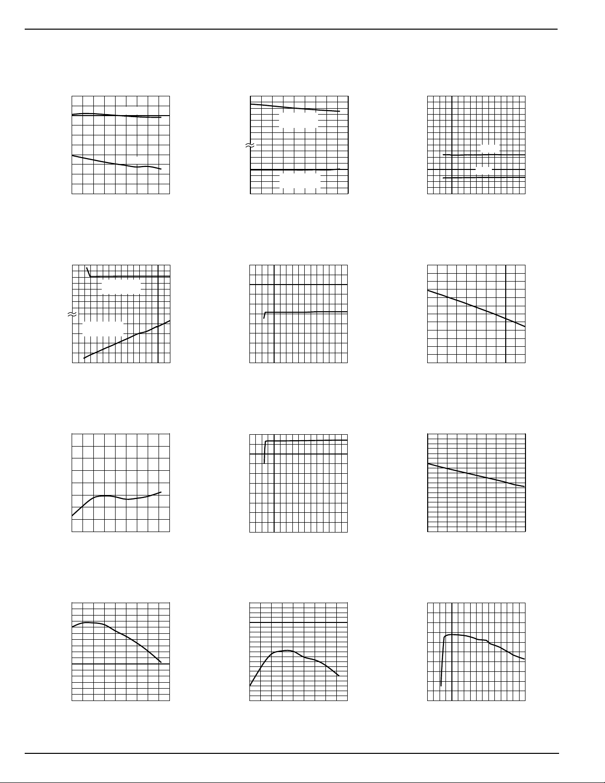
Typical Characteristics
Quiescent Current
2.0
1.8
1.6
1.4
1.2
1.0
0.8
0.6
CURRENT (mA)
0.4
0.2
vs. Temperature
PWM
Skip
0
-40 -20 0 20 40 60 80 100120140
TEMPERATURE (°C)
Quiescent Current
vs. Supply Voltage
1.5
1.0
0.5
0
0.5
-0.5
0.4
CURRENT (µA)
0.3
0.2
0.1
0
0 4 8 12 16 20 24 28 32
UVLO Mode
(mA)
SHUTDOWN
(µA)
SUPPLY VOLTAGE (V)
Quiescent Current
1.50
1.00
0.50
mA
-0.50
0.20
0.15
CURRENT
0.10
0.05
1.256
1.254
1.252
1.250
1.248
1.246
1.244
1.242
1.240
1.238
REFERENCE VOLTAGE (V)
1.236
vs. Temperature
UVLO Mode
0
0
-40 -20 0 20 40 60 80 100120140
V
(mA)
SHUTDOWN
(
A)
TEMPERATURE (°C)
(Fixed Versions)
REF
Line Regulation
0 4 8 121620242832
SUPPLY VOLTAGE (V)
Quiescent Current
vs. Supply Voltage
4.0
3.5
3.0
2.5
2.0
1.5
CURRENT (mA)
1.0
0.5
0
0 4 8 121620242832
INPUT VOLTAGE (V)
V
REF
1.260
1.250
1.240
1.230
1.220
1.210
REFERENCE VOLTAGE (V)
1.200
Load Regulation
0 200 400 600 800 1000
LOAD CURRENT (µA)
PWM
Skip
(Fixed Versions)
V
(Fixed Versions)
REF
1.260
1.255
1.250
1.245
REFERENCE VOLTAGE (V)
1.240
4.98
4.96
4.94
4.92
4.90
4.88
4.86
REGULATOR VOLTAGE (V)
4.84
DD
V
4.82
vs. Temperature
-40 -20 0 20 40 60 80 100120140
TEMPERATURE (°C)
V
DD
vs. Temperature
-40 -20 0 20 40 60 80 100120140
TEMPERATURE (°C)
5.0
4.8
4.6
4.4
4.2
REGULATOR VOLTAGE (V)
DD
V
4.0
0 4 8 121620242832
Oscillator Frequency
10
8
6
4
2
0
-2
-4
-6
-8
FREQUENCY VARIATION (%)
-10
-40 -20 0 20 40 60 80 100120140
V
DD
Line Regulation
SUPPLY VOLTAGE (V)
vs. Temperature
TEMPERATURE (°C)
V
DD
5.00
4.95
4.90
4.85
REGULATOR VOLTAGE (V)
DD
V
4.80
Load Regulation
0 5 10 15 20 25
LOAD CURRENT (mA)
Oscillator Frequency
vs. Supply Voltage
1.0
0.8
0.6
0.4
0.2
0
-0.2
-0.4
-0.6
-0.8
FREQUENCY VARIATION (%)
-1.0
0 4 8 121620242832
SUPPLY VOLTAGE (V)
MIC2182 6 June 2000
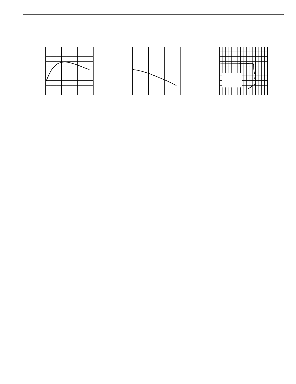
MIC2182 Micrel
0
1
2
3
4
5
012345678
OUTPUT VOLTAGE (V)
OUTPUT CURRENT (A)
Current-Limit
Foldback
VIN = 5V
V
OUT
= 3.3V
R
CS
= 15mΩ
Soft-Start Current
5.0
4.8
4.6
4.4
CURRENT (µA)
4.2
4.0
vs. Temperature
-40 -20 0 20 40 60 80 100120140
TEMPERATURE (°C)
Overcurrent Threshold
0.12
0.11
0.10
0.09
0.08
OVERCURRENT THRESHOLD (V)
vs. Temperature
-40 -20 0 20 40 60 80 100120140
TEMPERATURE (°C)
June 2000 7 MIC2182

MIC2182 Micrel
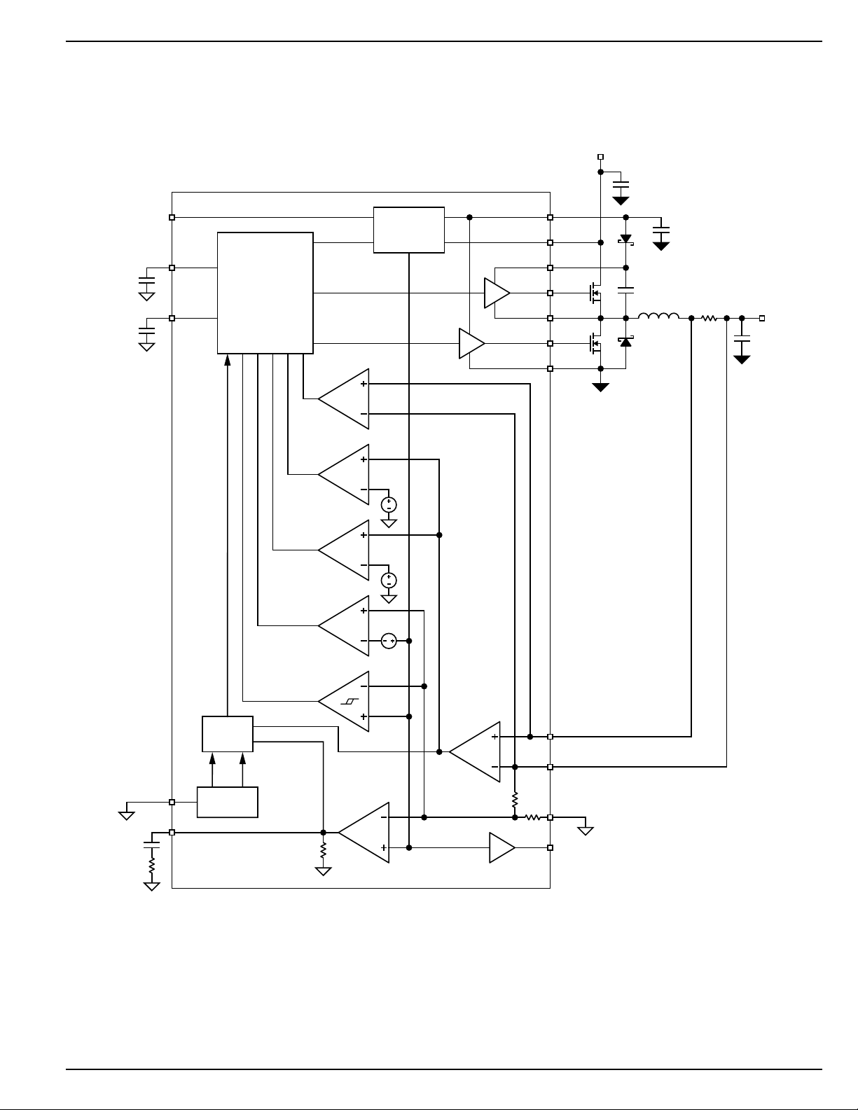
Block Diagrams
V
IN
C
IN
V
1.245V
DD
V
IN
EN/UVLO
6 11
SS
1
Control
Logic
PWM
2
Current
Limit
Reference
BG
V
VDD
VIN
10
VBST
14
HSD
16
VSW
15
LSD
13
PGND
12
Q2
Q1
D2
C
D1
BST
L1
4.7µF
R
CS
V
OUT
C
OUT
C
COMP
R
COMP
SYNC
COMP
RESET
Oscillator
5
3
MIC2182 [adj.]
PWM OUTPUT
PWM
CORRECTIVE
RAMP
PWM Mode
to Skip
Mode
Skip-Mode
Current
Limit
Low
Comp
Hysteresis
Comp
Error
Amp
100k
0.024V
0.07V
–2%V
BG
BG
V
= 0.2×10
G
m
Current
Sense
Amp
AV = 2
-3
CSH
8
VOUT
9
FB
7
SGND
4
R1
V 1.245V
=+
OUT
OUT(max)
= .0
V6V
1
R2
R1
R2
Figure 2a. Adjustable Output Voltage Version
MIC2182 8 June 2000
MIC2182 Micrel
Low
Comp
Current
Limit
Skip-Mode
Current
Limit
Hysteresis
Comp
V
BG
1.245V
V
BG
0.07V
–2%V
BG
Error
Amp
Control
Logic
V
IN
V
DD
PWM
PWM OUTPUT
CORRECTIVE
RAMP
RESET
Reference
Oscillator
0.024V
EN/UVLO
6 11
14
10
16
15
13
12
8
9
4
7
1
2
5
3
SS
PWM
SYNC
COMP
VREF
100k
G
m
= 0.2×10
-3
MIC2182-x.x
SGND
R2
50k
R1*
VOUT
CSH
VDD
VBST
C
IN
VIN
HSD
Q2
Q1
D1
D2
C
BST
R
CS
C
OUT
V
IN
V
OUT
L1
VSW
LSD
PGND
C
COMP
R
COMP
4.7µF
*82.5k for 3.3V Output
150k for 5V Output
AV = 2
Current
Sense
Amp
PWM Mode
to Skip
Mode
June 2000 9 MIC2182
Figure 2b. Fixed Output Voltage Versions
 Loading...