


General Description
MIC2172/3172
100kHz 1.25A Switching Regulators
Features
The MIC2172 and MIC317 2 are complete 100kHz SMPS
current-mode controllers with internal 65V 1.25A power
switches. The MIC2172 features external frequency
synchronization or frequency adjustment, while the
MIC3172 features an enable/shutdown control input.
Although primarily intended for voltage step-up
applications, the floating switch architecture of the
MIC2172/3172 mak es it practical for step-do wn, inverting,
and Cuk configurations as well as isolated topologies.
Operating from 3V to 40V, the MIC2 172/3172 draws only
7mA of quiescent current making it attractive for battery
operated supplies.
The MIC3172 is for appl ications that require on/of f control
of the regulator. The MIC3172 is externally shutdown by
applying a TTL low s ignal to EN (enable) . When disable d,
the MIC3172 draws only leakage current (typically less
than 1µA). EN must be high for normal operation. For
applications not requ ir in g c ontrol , EN must be tied to V
TTL high.
The MIC2172 is for applications requiring two or more
SMPS regulators that op erate from the same input su pply.
The MIC2172 features a S YNC input which allows loc king
of its internal oscillator to an external reference. This
makes it possible to avoid the audible beat frequencies
that result from the unequal oscillator frequencies of
independent SMPS regu lat or s .
A reference signal can be supplied by one MIC2172
designated as a master. To insure locking of the slave’s
oscillators, the reference oscillator frequency must be
higher than the slave’s. The master MIC2172’s oscillator
frequency is increased up to 135kHz by connecting a
resistor from SYNC to ground (see applications
information).
The MIC2172/3172 is ava ilable in an 8-pin plastic DIP or
SOIC for –40°C to +85°C operation.
IN or
• 1.25A, 65V internal switch rating
• 3V to 40V input voltage range
• Current-mode operation
• Internal cycle-by-cycle current limit
• Thermal shutdown
• Low external parts count
• Operates in most switching topologies
• 7mA quiescent current (operating)
• <1µA quiescent current, shutdown mode (MIC3172)
• TTL shutdown compatibility (MIC3172)
• External frequency synchronization (MIC2172)
• External frequency trim (MIC2172)
• Fits most LT1172 sockets (see applications info)
Applications
• Laptop/palmtop computers
• Toys
• Hand-held instruments
• Off-line converter up to 50W (requires external power
switch)
• Predriver for higher power capability
• Master/slave configurations (MIC2172)
___________________________________________________________________________________________________________
Micrel Inc. • 2180 Fortune Drive • San Jose, CA 95131 • USA • tel +1 (408) 944-0800 • fax + 1 (408) 474-1000 • http://www.micrel.com
April 2006
M9999-041806
(408) 955-1690
Micrel MIC2172/3172
Typical Applications
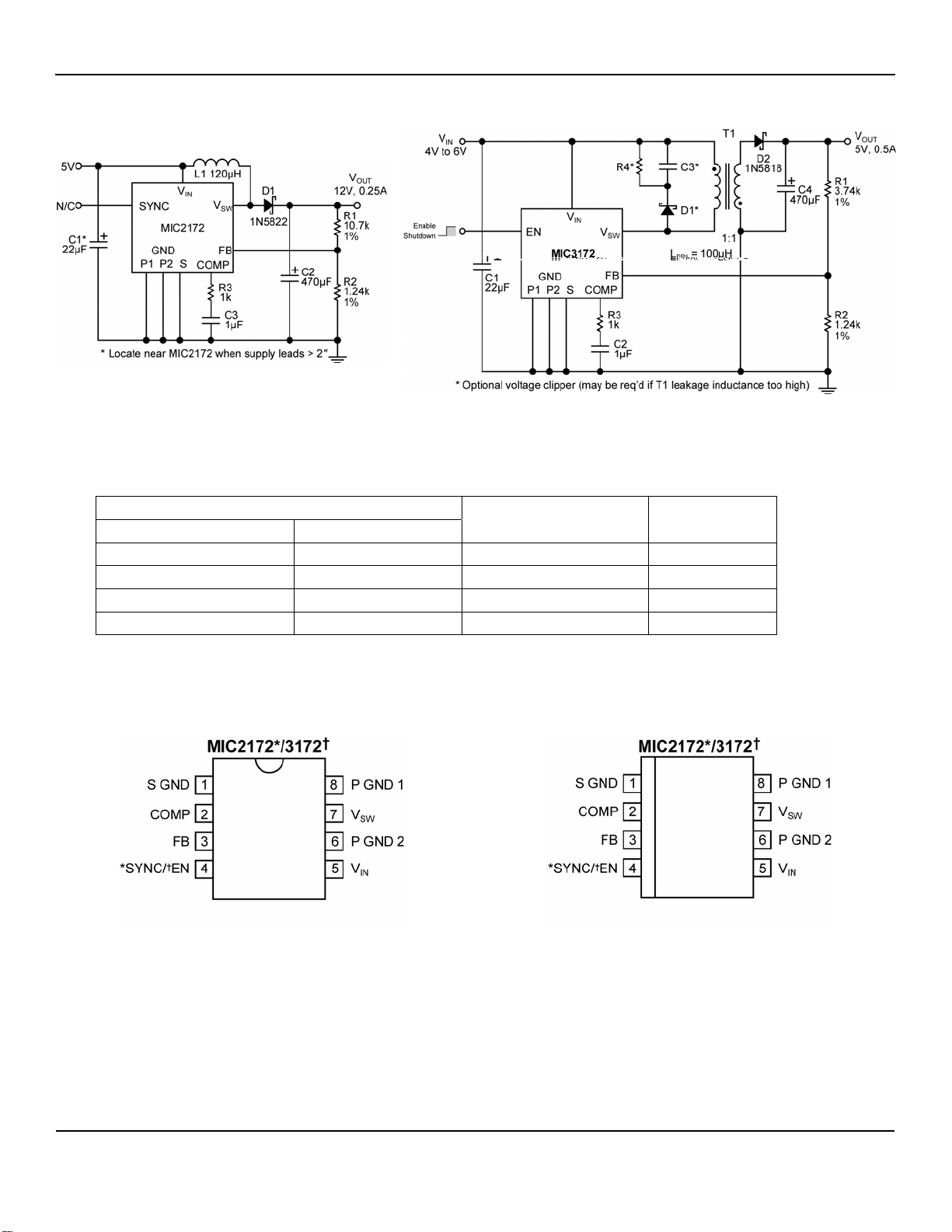
Figure 1. MIC2172 5V to 12V Boost Converter
Ordering Information
Part Number
Standard Pb-Free
MIC2172BN MIC2172YN –40°C to +85°C 8-pin plastic DIP
MIC2172BM MIC2172YM –40°C to +85°C 8-pin SOIC
MIC3172BN MIC3172YN –40°C to +85°C 8-pin plastic DIP
MIC3172BM MIC3172YM –40°C to +85°C 8-pin SOIC
Note:
1. Other Voltage available. Contact Micrel for details.
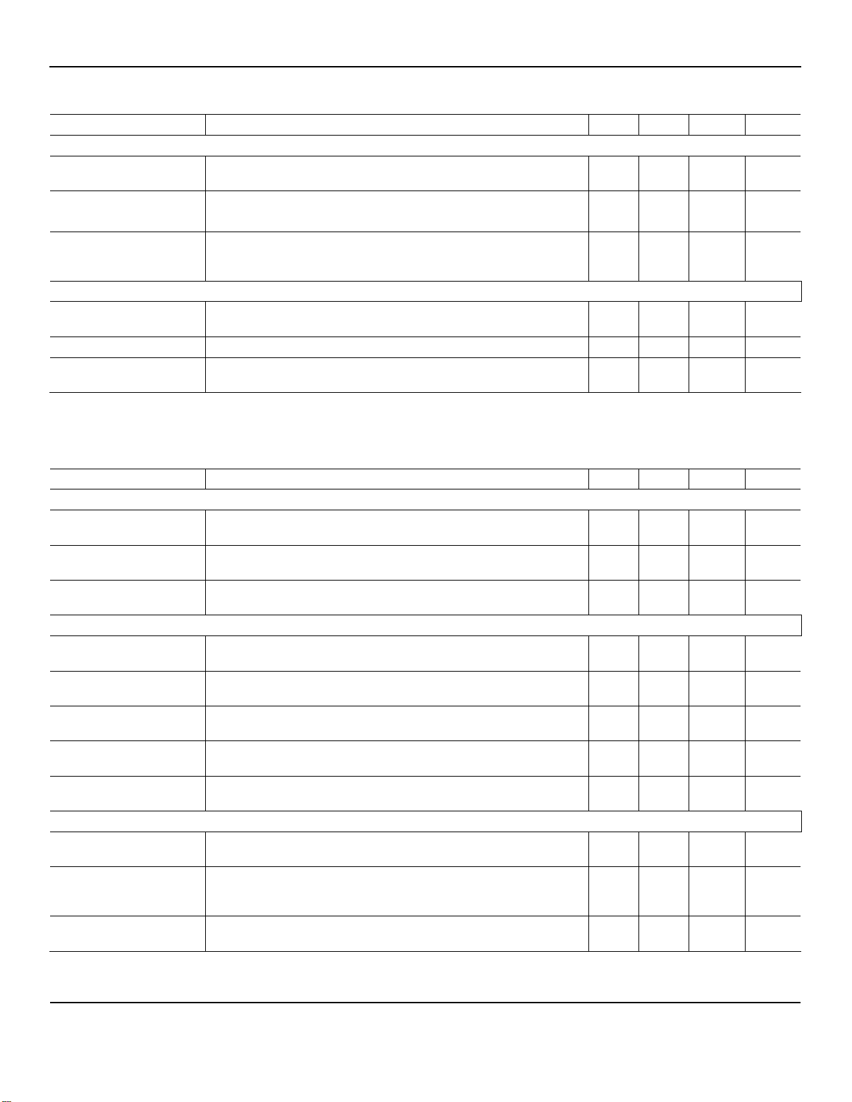
Pin Configuration
Figure 2. MIC3172 Flyback Converter
Junction Temp. Range Package
8-pin DIP (N) 8-pin SOIC (M)
April 2006 2
M9999-041806
(408) 955-1690

Micrel MIC2172/3172
Pin Description
Pin Number Pin Name Pin Function
1 S GND Signal Ground: Internal analog circuit ground. Connect directly to the input filter
capacitor for proper operation (see applications info). Keep separate from power
grounds.
2 COMP Frequency Compensation: Output of transconductance type error amplifier.
Primary function is for loop stabilization. Can also be used for output voltage
soft-start and current limit tailoring.
3 FB Feedback: Inverting input of error amplifier. Connect to external resistive divider
to set power supply output voltage.
4 (MIC2172) SYNC Synchronization/Frequency Adjust: Capacitively coupled input signal greater
than device’s free running frequency (up to 135kHz) will lock device’s oscillator
on falling edge. Oscillator frequency can be trimmed up to 135kHz by adding a
resistor to ground. If unused, pin must float (no connection).
4 (MIC3172) EN Enable: Apply TTL high or connect to VIN to enable the regulator. Apply TTL low
or connect to ground to disable the regulator. Device draws only leakage current
(<1µA) when disabled.
5 VIN Supply Voltage: 3.0V to 40V
6 P GND 2
7 VSW Power Switch Collector: Collector of NPN switch. Connect to external inductor or
8 P GND 1
Power Ground #2: One of two NPN power switch emitters with 0.3
sense resistor in series. Required. Connect to external inductor or input voltage
ground depending on circuit topology.
input voltage depending on circuit topology.
Power Ground #1: One of two NPN power switch emitters with 0.3
sense resistor in series. Optional. For maximum power capability connect to P
GND 2. Floating pin reduces current limit by a factor of two.
Ω current
Ω current
April 2006 3
M9999-041806
(408) 955-1690
Micrel MIC2172/3172
Absolute Maximum Ratings MIC2172
Input Voltage.................................................................. 40V
Switch Voltage............................................................... 65V
Sync Current............................................................... 50mA
Feedback Voltage (Transient, 1ms) ............................ ±15V
Operating Temperature Range
8-pin PDIP.................................................–40 to +85 °C
8-pin SOIC ................................................–40 to +85°C
Junction Temperature................................–55°C to +150°C
Thermal Resistance
θ
θ
8-pin PDIP................................................. 130°C/W
JA
8-pin SOIC................................................. 120°C/W
JA
Storage Temperature ................................–65°C to +150°C
Soldering (10 sec.) ...................................................+300°C
Electrical Characteristics MIC2172
Note 1, 3. Unless otherwise specified, V
Parameter Condition Min Typ Max Units
Reference Section
Feedback Voltage (VFB) 1.220
Feedback Voltage Line
Regulation
Feedback Bias Current
)
(I
FB
Error Amplifier Section
Transconductance
/∆VFB)
(∆I
COMP
Voltage Gain
COMP
/∆VFB)
(∆V
Output Current V
Output Swing High Clamp, VFB = 1V
Compensation Pin
Threshold
ON Resistance ISW = 1A, VFB = 0.8V 0.76 1
Current Limit Duty Cycle = 50%, TJ ≥ 25°C
Breakdown Voltage (BV) 3V ≤ VIN ≤ 40V
Notes:
1. Exceeding the absolute maximum rating may damage the device.
2. The device is not guaranteed to function outside its operating rating.
3. Devices are ESD sensitive. Handling precautions recommended. Human body model, 1.5k in series with 100pF.
4. Specification for packaged product only.
Pin 2 tied to pin 3
3V ≤ VIN ≤ 40V
310 750
∆I
= ±25µA 3.0
COMP
0.9V ≤ V
= 1.5V 125
COMP
Low Clamp, V
Duty Cycle = 0 0.8
Duty Cycle = 50%, TJ < 25°C
Duty Cycle = 80%, Note 2
= 5mA
I
SW
IN = 5V.
1.240 1.264
1.214
1.274
0.03
1100
3.9 6.0
2.4
≤ 1.4V 500 800 2000 V/V
COMP
7.0
175 350
= 1.5V
FB
100
1.8
0.25
2.1
0.35
400
2.3
0.52
0.9 1.08
0.6
1.25
Output Switch Section
1.1
1.25
1.25
1
65
75 V
3
3.5
2.5
V
V
%/V
nA
nA
µA/mV
µA/mV
µA
µA
V
V
V
V
Ω
Ω
A
A
A
April 2006 4
M9999-041806
(408) 955-1690
Micrel MIC2172/3172
Typical Characteristics MIC2172 (cont)
Parameter Condition Min Typ Max Units
Oscillator Section
Frequency (fO) 88
Duty Cycle [δ(max)]
100 112
85
80 89
115
95
kHz
kHz
%
Sync Coupling Capacitor
Required for Frequency
VPP = 3.0V
= 40V
V
PP
22
2.2
51
4.7
120
10
pF
pF
Lock
Input Supply Voltage Section
Minimum Operating
2.7
3.0
V
Voltage
Quiescent Current (IQ) 3V ≤ VIN ≤ 40V, V
Supply Current Increase
)
(∆I
IN
∆I
= 1A, V
SW
COMP
= 0.6V, ISW = 0 7
COMP
= 1.5V 9 20 mA
9
mA
Electrical Characteristics MIC3172
Note 1, 3. Unless otherwise specified, V
IN = 5V.
Parameter Condition Min Typ Max Units
Reference Section
Feedback Voltage (VFB) 1.224
Feedback Voltage Line
Pin 2 tied to pin 3
1.240 1.264
1.214
3V ≤ VIN ≤ 40V 0.07
1.274
%/V
V
V
Regulation
Feedback Bias Current
)
(I
FB
310 750
1100
nA
nA
Error Amplifier Section
Transconductance
/∆VFB)
(∆I
COMP
Voltage Gain
COMP
/∆VFB)
(∆V
Output Current V
Output Swing High Clamp, VFB = 1V
Compensation Pin
Threshold
∆I
= ±25µA 3.0
COMP
2.4
0.9V ≤ V
COMP
≤ 1.4V 500 800 2000 V/V
COMP
= 1.5V 125
100
1.8
Low Clamp, V
= 1.5V
FB
0.25
Duty Cycle = 0 0.8
0.6
3.9 6.0
7.0
175 350
400
2.1
0.35
2.3
0.52
0.9 1.08
1.25
µA/mV
µA/mV
µA
µA
V
V
V
V
Output Switch Section
ON Resistance ISW = 1A, VFB = 0.8V 0.76 1
1.1
Current Limit Duty Cycle = 50%, TJ ≥ 25°C
Duty Cycle = 50%, TJ < 25°C
Duty Cycle = 80%, Note 2
Breakdown Voltage (BV) 3V ≤ VIN ≤ 40V
= 5mA
I
SW
1.25
1.25
1
65
3.5
2.5
75 V
3
Ω
Ω
A
A
A
April 2006 5
M9999-041806
(408) 955-1690

Micrel MIC2172/3172
Typical Characteristics MIC3172 (cont)
Parameter Condition Min Typ Max Units
Oscillator Section
Frequency (fO) 88
Duty Cycle [δ(max)]
100 112
85
80 89
115
95
kHz
kHz
%
Sync Coupling Capacitor
Required for Frequency
VPP = 3.0V
= 40V
V
PP
22
2.2
51
4.7
120
10
pF
pF
Lock
Input Supply Voltage Section and Enable Section
Minimum Operating
2.7
3.0
V
Voltage
Quiescent Current (IQ) 3V ≤ VIN ≤ 40V, V
Supply Current Increase
)
(∆I
IN
∆I
= 1A, V
SW
COMP
= 0.6V, ISW = 0 7
COMP
= 1.5V 9 20 mA
Enable Input Threshold
Enable Input Current VEN = 0V
= 2.4V
V
EN
Bold type denotes specifications applicable to the full operating temperature range.
Note 1. Devices are ESD sensitive. Handling precautions required.
Note 2. For duty cycles (δ) between 50% and 95%, minimum guaranteed switch current is given by I
Note 3. Specification for packaged product only.
0.4
1.2
–1 0
2
= 0.833 (2- δ) for the MIC3172.
CL
9
2.4
1
10
mA
V
µA
µA
April 2006 6
M9999-041806
(408) 955-1690

Micrel MIC2172/3172
Typical Characteristics
April 2006 7
M9999-041806
(408) 955-1690

Micrel MIC2172/3172
Typical Characteristics (cont.)
April 2006 8
M9999-041806
(408) 955-1690

Micrel MIC2172/3172
Functional Characteristics
MIC2172 Block Diagram
MIC3172 Block Diagram
April 2006 9
M9999-041806
(408) 955-1690

Micrel MIC2172/3172
Functional Description
Refer to “Block Diagram MIC2172” and “Block Diagram
MIC3172.”
Internal Power
The MIC2172/3172 operates when V
EN ≥ 2.0V for the MIC317 2). An internal 2.3V regulator
V
supplies biasing to all internal circuitry including a
precision 1.24V band gap reference.
The enable control (MIC 3172 only) enables or disables
the internal regulator which supplies power to all other
internal circuitry.
PWM Operation
The 100kHz oscillator generates a signal with a duty
cycle of approximately 90%. The current-mode
comparator output is us ed t o r ed uc e th e d uty cycle when
the current amplifier output voltage exceeds the error
amplifier output voltage. The resulting PWM signal
controls a driver which supplies base current to output
transistor Q1.
Current Mode Advantages
The MIC2172/3172 operate s in cur rent mode r ather than
voltage mode. There are three distinct advantages to
this technique. Feedback loop compensation is greatly
IN is ≥ 2.6V (and
simplified because inductor current sensing removes a
pole from the closed loop response. Inherent cycle-bycycle current limiting gre atly improves the power switch
reliability and pr ovides automatic output current limiting.
Finally, current-m ode operatio n provides a utomatic i nput
voltage feed for ward whic h prevents inst antaneous input
voltage changes from disturbing the output voltage
setting.
Anti-Saturation
The anti-saturation dio de (D1) increases the usable d uty
cycle range of the MIC2172/3172 by eliminating the
base to collector stored charge which would delay Q1’s
turnoff.
Compensation
Loop stability compensation of the MIC2172/3172 can
be accomplished b y connecting an appropriate network
from either COMP to circuit ground (Typical
Applications) or COMP to FB.
The error amplif ier output (COMP) is also useful for s oft
start and current limiting. Because the error amplifier
output is a transconduc tance type, the output impedance
is relatively high which m eans the outp ut volta ge can be
easily clamped or adjusted externally.
April 2006 10
M9999-041806
(408) 955-1690

Micrel MIC2172/3172
Application Information
Using the MIC3172 Enable Control (New Designs)
For new designs requiring enable/shutdown control,
connect EN to a T TL or CMOS control signal (figure 3).
The very low driver current requirement ensures
compatibility regardless of the driver or gate used.
Figure 3. MIC3172 TTL Enable/Shutdown
Using the MIC3172 in LT1172 Applications
The MIC3172 can be used in most original LT1172
applications by adapting the MIC3172’s
enable/shutdown feature to the existing LT1172 circuit.
Unlike the LT1172 wh ich can be shutdown by reducing
the voltage on pin 2 (V
) below 0.15V, the MIC 3172 has
C
a dedicated enable/shutdown pin. To replace the
LT1172 with the MIC3172, determine if the LT1172’s
shutdown feature is used.
By using the MIC3172, U1 and Q1 shown in figure 5 can
be eliminated, reducing the total components count.
Synchronizing the MIC2172
Using several unsynchronized switching regulators in the
same circuit will cause beat frequencies to appear on the
inputs and outputs. T hese beat frequencies can be very
low making them difficult to filter.
Micrel’s MIC2172 can be synchronized to a single
master frequenc y avoiding the possibility of undes irable
beat frequencies in multiple regulator circuits. The
master frequency can be an external oscillator or a
designated master MIC2172. The master frequency
should be 1.05 to 1.20 tim es the s lave’s 1 00k Hz nominal
frequency to guarantee synchronization.
Circuits without Shutdown
If the shutdown featur e is not being used, c onnect EN to
V
IN to continuously enable the MIC3172 or use an
MIC2172 with
SYNC open (figure 4).
Figure 4. MIC2172/3172 Always Enabled
Circuits with Shutdown
If shutdown was used in th e original LT 1172 applicat ion,
connect EN to a logic gate that produces a TTL logiclevel output signal that matches the shutdown signal.
The MIC3172 will be enabled b y a logic-high input and
shutdown with a logic-low input (figure 5). The actual
components perform ing the functions of U1 and Q1 ma y
vary according to the original application.
Figure 6. Master/Slave Synchronization
Figure 6 shows a typical application where several
MIC2172s operate from the same supply voltage. U1’s
oscillator frequenc y is incre ased abo ve U2’s and U3’s by
connecting a resistor from SYNC to ground. U2-SYNC
and U3-SYNC are capacitively coupled to the master’s
output (V
). The slaves lock to the negative (falling
SW
edge) of U1’s output waveform.
Figure 5. Adapting to the LT1172 Socket
April 2006 11
Figure 7. External Synchronization
Care must be exercised to insure that the master
MIC2172 is always operating in continuous mode.
Figure 7 shows how one or more MIC2172s can be
M9999-041806
(408) 955-1690

Micrel MIC2172/3172
locked to an external reference frequency. The slaves
lock to the negative (falling edge) of the external
reference waveform.
Soft Start
A diode-coupled c apacitor from COMP to circu it ground
slows the output voltage rise at turn on (figure 8).
Figure 8. Soft Start
The additional time it takes for the error amplifier to
charge the capacitor cor responds to the tim e it takes the
output to reach regulation. Diode D1 discharges C1
when V
IN is removed.
Another soft start circuit is shown in figure 8A. The
circuit uses capacitor C1 to c ontrol th e output risetime b y
providing feedback from the output to the FB pin. The
output voltage starts to rise when the MIC31 72 regu lator
starts switching. T his is the dv/dt of the outpu t will for ce
a current through ca pacitor C1, which flo ws through the
lower feedback resistor, R2, increasing the voltage on
the FB pin. This increased voltage on the FB pin
reduces the duty cycle at th e V
pin, limiting the turn- on
SW
time of the output. Increasing the value of C1 causes
the output voltage to rise more slowly. Diode D1 is
reverse biased in normal operation and prevents C1
from appearing in parall el with the upper voltage d ivider
resistor, which would affect stability and transient
response. Zener diode D 2 clamps the voltage s een by
the feedback pin and pr ovides a discharge path for C1
when the power supply is turned off.
Current Limit
For designs demanding less output current than the
MIC2172/3172 is c apable of deliver ing, P GN D 1 c an be
left open reducing the current capability of Q1 by onehalf.
Figure 8b. Without Soft Start
Figure 8c. With Soft Start
Figure 8a. Additional Soft Start Circuit
This circuit onl y limits the dv/dt of the output when the
boost converter is runn ing. It will not decreas e the dv/dt
or the initial inrush ca used by appl ying the input v oltage.
Figure 8B shows the turn-on without a soft start circuit
and Figure 8C shows how the s oft start circuit reduces
inrush and prevents output voltage overshoot.
April 2006 12
Figure 9. Current Limit
Alternatively, the maximum current limit of the
MIC2172/3172 can be reduced by adding a voltage
M9999-041806
(408) 955-1690

Micrel MIC2172/3172
clamp to the COMP output (figure 9). This feature can be
useful in applications requiring either a complete
shutdown of Q1’s switching action or a form of current
fold-back lim iting. T his use of the COMP o utput do es n ot
disable the oscillator, amplifiers or other circuitry,
therefore the supply current is never less than
approximately 5mA.
Thermal Management
Although the MIC2172/3172 family contains thermal
protection circuitry, for best reliability, avoid prolonged
operation with junction temperatures near the rated
maximum.
The junction temperature is determined by first
calculating the power dissipation of the device. For the
MIC2172/3172, the tota l power dissipation is the sum of
the device operating losses and power switch losses.
The device operating losses are the dc losses
associated with biasing all of the internal functions plus
the losses of the power switch driver circuitry. The dc
losses are calculat ed from the supply voltage (V
device supply current (I
). The MIC2172/3172 supply
Q
) and
IN
current is almost constant regardless of the supply
voltage (see “Electrical Characteristics”). The driver
section losses (not inc ludin g the s witch) are a f unction of
supply voltage, power switch current, and duty cycle.
()
+
()
⎡
+=
⎢
⎣
⎛
IVI VP
⎜
SWINQINdriverbias
50
⎝
⎤
+
δ0.004
⎞
⎟
⎥
⎠
⎦
where:
P
(bias+driver)
V
IN
I
= quiescent supply current
Q
I
SW
= device operating losses
= supply voltage
= power switch current
(see “Design Hints: Switch Current Calculations”)
δ = duty cycle
VVV
±+
V
V
δ
=
= output voltage
OUT
= D1 forward voltage drop
F
INFOUT
VV
+
FOUT
As a practical example refer to figure 1.
V
= 5.0V
IN
I
= 0.006A
Q
I
= 0.625A
SW
δ = 60% (0.6)
Then:
driverbias
+
()
()
driverbias
+
()
0.068WP
=
Power switch dissipation calculations are greatly
simplified by mak ing two assumptions which are usu ally
fairly accurate. First, the majority of loss es in the power
switch are due to on-loss es. To find thes e los ses, as si gn
a resistance value to the collector/emitter terminals of
the device using the satur ation voltage versus collector
current curves (see Typical Performance
Characteristics). Power switch losses are calculated by
modeling the switch as a resistor with the switch duty
cycle modifying the average power dissipation.
= (ISW)2 RSW δ
P
SW
From the Typical performance Characteristics:
R
= 1Ω
SW
Then:
P
= (0.625)2 × 1 × 0.6
SW
= 0.234W
P
SW
= 0.068 + 0.234
P
(total)
= 0.302W
P
(total)
The junction temperature for any semiconductor is
calculated using the following:
T
= TA + P
J
(total) θJA
Where:
T
= junction temperature
J
= ambient temperature (maximum)
T
A
= total power dissipation
P
(total)
θ
= junction to ambient thermal resistance
JA
For the practical example:
T
= 70°C
A
θ
= 130°C/W (for plastic DIP)
JA
Then:
T
= 70 + 0.30 ⋅ 130
J
T
= 109°C
J
This junction temperature is below the rated maximum of
150°C.
Grounding
Refer to figure 10. Heavy lines indicate high current
paths.
⎡
⎛
0.62550.0065P
+×=
⎜
⎢
⎝
⎣
50
0.60.004
+
⎞
⎟
⎠
⎤
⎥
⎦
April 2006 13
M9999-041806
(408) 955-1690

Micrel MIC2172/3172
L1 is operating in continuous mode if it does not
discharge completely before the MIC2172/3172 power
switch is turned on again.
Discontinuous Mode Design
Given the maximum output current, solve equation ( 1) to
determine whether the device can operate in
discontinuous m ode without initiat ing the internal de vice
current limit.
I
⎞
⎛
Figure 10. Single Point Ground
A single point ground is strongly recommended for
proper operation.
The signal ground, compensation network ground, and
feedback network connections are sensitive to minor
voltage variations. The input and output capacitor
grounds and power ground conductors will exhibit
voltage drop when carrying large currents. Keep the
sensitive circuit gro und traces separate from the power
ground traces. Small voltage variations applied to the
sensitive circuits c an prevent the MIC2172/3172 or any
switching regulator from functioning properly.
Applications and Design Hints
Access to both the collector and emitter(s) of the NPN
power switch makes the MIC2172/3172 extremely
versatile and suita ble f or us e in most PWM power supply
topologies.
Boost Conversion
Refer to figure 11 for a typical boost conversion
application where a +5V logic supply is available but
+12V at 0.14A is required.
Figure 11. 5V to 12V Boost Converter
The first step in designing a boost converter is
determining whether induc tor L1 will caus e the con verter
to operate in either continuous or discontinuous mode.
Discontinuous m ode is preferred because the f eedback
control of the converter is simpler.
When L1 discharges its current completely during the
MIC2172/3172’s off -time, it is opera ting in disconti nuous
mode.
April 2006 14
CL
⎜
2
I
δ
⎝
≤ (1)
OUT
V
= (1a)
Where:
I
= internal switch current limit
CL
= 1.25A when δ < 50%
I
CL
I
= 0.833 (2 – δ) when δ ≥ 50%
CL
(Refer to Electrical Characteristics.)
= maximum output current
I
OUT
= minimum input voltage
V
IN
δ = duty cycle
= required output volta ge
V
OUT
= D1 forward voltage drop
V
F
For the example in figure 11.
I
= 0.14A
OUT
= 1.147A
I
CL
= 4.75V (minimum)
V
IN
δ = 0.623
V
= 12.0V
OUT
= 0.6V
V
F
Then:
1.147
⎛
⎜
⎝
≤
I
OUT
0.141AI
≤
OUT
This value is greater than the 0.14A output current
requirement so we can proceed to find the inductance
value of L1.
()
L1≤ (2)
IN
Where:
P
= 12 ⋅ 0.14 = 1.68W
OUT
f
SW
= 1⋅10
5
For our practical example:
δ V
⎟
IN
⎠
OUT
VVV
±+
INFOUT
VV
+
FOUT
⎞
⎟
2
⎠
××
12
2
δ V
f P 2
SWOUT
kHz (100kHz)
0.6234.75
M9999-041806
(408) 955-1690

Micrel MIC2172/3172
()
L1
≤
≤ 26.062µH (use 27µH)
I
L1
×
2
0.6234.75
5
1011.682
×××
Equation (3) solves for L1’s maximum current value.
T V
I
L1(peak)
= (3)
ONIN
L1
Where:
= δ / fSW = 6.23×10⁻⁶ sec
T
ON
6
−
106.234.75
I
L1(peak)
I
L1(peak)
=
= 1.096A
××
6
−
1027
×
Use a 27µH inductor with a peak current rating of at
least 1.4A.
Flyback Conversion
Flyback converter topology may be used in low power
applications where voltage isolation is required or
whenever the input vo ltage can be less than or greater
than the output voltage. As with the step-up converter
the inductor (transformer primary) current can be
continuous or disconti nuous. Discontinuous operat ion is
recommended.
Figure 12 shows a practical flyback converter design
using the MIC3172.
Switch Operation
During Q1’s on time ( Q1 is the intern al NPN transis tor—
see block diagrams), energy is stored in T1’s primary
inductance. During Q1’s off time, stored energy is
partially discharged into C4 (output filter capacitor).
Careful selection of a low ESR capacitor for C4 may
provide satisfactory output ripple voltage making
additional filter stages unnecessary.
C1 (input capacitor) may be red uced or elim inated if t he
MIC3172 is located near a low impedance voltage
source.
Output Diode
The output diode allows T 1 to store ener gy in its prim ary
inductance (D2 nonco nducting) and release energ y into
C4 (D2 conducting). T he low forward voltage drop of a
Schottky diode minimizes power loss in D2.
Frequency Compensation
A simple frequenc y compensation network consisting of
R3 and C2 prevents output oscillations.
High impedance output stages (transconductance type)
in the MIC2172/3172 often perm it sim plified lo op-s tabil ity
solutions to be connected to circuit ground, although a
more conventional technique of connecting the
components from the error amplifier output to its
April 2006 15
inverting input is also poss i ble.
Voltage Clipper
Care must be taken to minimize T1’s leakage
inductance, otherwise it may be necessary to
incorporate the volta ge clipper c onsisting of D1, R4, a nd
C3 to avoid second breakdown (failure) of the
MIC3172’s power NPN Q1.
Enable/Shutdown
The MIC3172 includes the enable/shutdown feature.
When the device is s h utdo wn, total suppl y curren t is l ess
than 1µA. This is ideal for battery applications where
portions of a system ar e powered only when needed. If
this feature is not r equired, simpl y connect EN to V
to a TTL high voltage.
Discontinuous Mode Design
When designing a discontinuous flyback converter , first
determine whether the device can safely handle the
peak primary current dem and placed on it by the output
power. Equation (8) finds the maximum duty cycle
required for a given input voltage and output power. If
the duty cycle is greater than 0.8, discontinuous
operation cannot be used.
δ ≥
VI
OUT
IN(min)CL
(8)
P 2
For a practical example let:
= 5.0V × 0.25A = 1.25W
P
OUT
= 4.0V to 6.0V
V
IN
I
= 1.25A when δ < 50%
CL
Then:
1.252
×
δ
≥
≥ 0.5 (50%) Use 0.55.
δ
41.25
×
The slightly hig her dut y cycle valu e is used to overco me
circuit ineffic iencies. A f ew iterat ions of equati on (8) m ay
be required if the dut y cycle is found to be greater than
50%.
Calculate the maximum transformer turns ratio
N
PRI/NSEC
, that will guarantee safe operation of the
a, or
MIC2172/3172 power switch.
VF V
a±≤ (9)
V
IN(max)CECE
SEC
Where:
a = transformer maximum turns ratio
= power switch collector to emitter maximum
V
CE
voltage
M9999-041806
(408) 955-1690
IN or

Micrel MIC2172/3172
F
= safety derating factor (0.8 for most
CE
commercial and industrial applications)
= maximum input voltage
V
IN(max)
= transformer secondary voltage (V
V
SEC
OUT
+ V
)
F
For the practical example:
V
= 65V max. for the MIC2172/3172
CE
= 0.8
F
CE
= 5.6V
V
SEC
Then:
a±×≤
a
≤ 8.2143
6.00.865
5.6
Next, calculate the maximum primary inductance
required to store th e neede d output energ y with a po wer
switch duty cycle of 55%.
2
2
T Vf 0.5
ON
L ≤ (10)
PRI
P
IN(min)SW
OUT
Where:
L
= maximum primary inductance
PRI
= device switching frequency (100kHz)
f
SW
= minimum input voltage
V
IN(min)
= power switch on time
T
ON
Then:
2
−
≤
L
PRI
L
PRI ≤ 19.23µH
()
1.25
625
105.54.01010.5
××××
Use an 18µH primary inductance to overcome circuit
inefficiencies.
To complete the design the inductance value of the
secondary is found which will guar antee that the energy
stored in the transformer during the power switch on
time will be completed disc harged into the output dur ing
the off-time. This is necessary when operating in
discontinuous-mode.
2
2
T Vf 0.5
OFF
L ≤ (11)
SEC
P
SECSW
OUT
Where:
L
= maximum secondary inductance
SEC
= power switch off time
T
OFF
Then:
2
−
625
104.55.61010.5
×××××
L
≤
L
SEC
SEC
≤ 25.4µH
1.25
()
Figure 12. MIC3172 5V 0.25A Flyback Converter
April 2006 16
M9999-041806
(408) 955-1690

Micrel MIC2172/3172
Finally, recalculate the transform er turns ratio to insure
that it is less than the value earlier found in equation (9).
L
L
PRI
SEC
a ≤ (12)
Then:
5
−
101.8
a
≤
×
5
−
102.54
×
a ≤ 0.84 Use 0.8 (same as 1:1.25).
This ratio is less than th e ratio ca lcula ted in equat ion ( 9).
When specifying the tra nsform er it is necessar y to know
the primary peak current which must be withstood
without saturating the transformer core.
T V
I =
PEAK(pri)
ONIN(min)
L
PRI
So:
6
−
××
I
PEAK(pri)
I
PEAK(pri)
= (13)
= 1.22A
105.54.0
18µ8
Now find the minimum reverse voltage requirement for
the output rectifier. This rectifier must have an avera ge
current rating greater th an the maximum output current
of 0.25A.
a
VV
()
V+≥ (14)
BR
OUTIN(max)
a
F
BR
Where:
V
= output rectifier maximum peak reverse
BR
voltage rating
a = transformer turns ratio (0.8)
F
= reverse voltage safety derating factor (0.8)
BR
Then:
()
0.85.06.0
V
≥
BR
15.625VV
≥
BR
×+
0.80.8
×
A 1N5817 will safely handle voltage and current
requirements in this example.
Forward Converters
Micrel’s MIC2172/3172 can be used in several circuit
configurations to generate an output voltage which is
less than the input voltage ( buck or step-down to polog y).
Figure 13 shows the MIC3172 in a voltage step-down
application. Beca use of the internal ar chitecture of these
devices, more external components are required to
implement a step-down r egulat or than with other dev ices
offered by Micrel (r efer to the LM257x or LM457x family
of buck switchers). However, for step-down conversion
April 2006 17
requiring a transf orm er (f orward), th e MIC2 172/31 72 i s a
good choice.
A 12V to 5V step-down converter using transformer
isolation (forward) is shown in figure 14. Unlike the
isolated flyback converter which stores energy in the
primary inductance during the controller’s on-time and
releases it to the load during the off-time, the forward
converter transfers energy to the output during the ontime, using the off-tim e to reset the transformer core. In
the application shown, the transformer core is reset by
the tertiary winding discharging T1’s peak magnetizing
current through D2.
For most forward converte rs the duty cycle is limited to
50%, allowing the transf ormer flux to reset with only two
times the input voltage appearing across the power
switch. Although during normal operation this circuit’s
duty cycle is well below 50%, the MIC2172 (and
MIC3172) has a maximum dut y cycle capability of 90 %.
If 90% was required dur ing operation (start-up and hi gh
load currents), a complete reset of the transformer
during the off -time would require the voltage across t he
power switch to be ten times the input voltage. This
would limit the input voltage to 6V or less for forward
converter applications.
To prevent core saturation, the application given here
uses a duty cycle limiter consisting of Q1, C4 and R3.
Whenever the MIC3172 exceeds a duty cycle of 50%,
T1’s reset winding current turns Q1 on. This action
reduces the dut y cycle of the MIC3172 unti l T1 is abl e to
reset during each cycle.
Fluorescent Lamp Supply
An extremely useful application of the MIC3172 is
generating an ac voltage f or fluorescent lamps used as
liquid crystal display back lighting in portable computers.
Figure 15 shows a complete po wer supply for lighting a
fluorescent lamp. Transistors Q1 and Q2 together with
capacitor C2 form a Royer oscillator. The Royer
oscillator generates a sine wave whose frequency is
determined by the ser i es L/ C c irc uit c omprised of T1 and
C2. Assuming that the MIC3172 and L1 ar e absent, and
the transistors’ emitters are grounded, circuit operation is
described in “Oscillator Operation.”
Oscillator Operation
Resistor R2 provides initial base current that turns
transistor Q1 on and im presses the inp ut voltage acro ss
one half of T1’s primary winding (Pri 1). T1’s feedba ck
winding provides additional base drive (positive
feedback) to Q1 f or c ing it well in to s at ur ation for a peri od
determined by the Pri 1/C2 time constant. Once the
voltage across C2 has reached its maximum circuit
value, Q1’s collector current will no longer increase.
Since T1 is in s er ies with Q1, this drop in pr imary current
causes the flux in T1 to change and because of the
M9999-041806
(408) 955-1690

Micrel MIC2172/3172
Figure 13. Step-Down or Buck Regulator
mutual coupling to t he feedback windin g further reduc es
primary current eventually turning Q1 off. The primary
windings now change state with the feedback winding
forcing Q2 on re peating the alternate half cycle ex actly
as with Q1. This action produces a sinusoidal voltage
wave form; whose amplit ude is proportional to the i nput
voltage, across T1’s primary winding which is stepped
up and capacitively coupled to the lamp.
Lamp Current Regulation
Initial ionization (lighting) of the fluorescent lamp
requires several times the ac voltage across it than is
required to sustain current through the device. The
current through the lamp is sampled and regulated by
the MIC3172 to achie ve a given intensit y. The MIC3172
uses L1 to maintain a constant average curr ent through
the transistor em itters. This current controls the voltage
amplitude of the Ro yer osci llator and m ainta ins the lam p
current. During the negative half cycle, lamp current is
rectified by D3. During the positive half cycle, lamp
current is rectified b y D2 thr ough R4 and R5. R3 a nd C5
filter the voltage dropped across R4 and R5 to the
MIC3172’s feedback pin. The MIC3172 maintains a
constant lamp curr ent by adjusting its duty cycle to k eep
the feedback voltag e at 1.24V. The intens ity of the lam p
is adjusted using potentiometer R5. The MIC3172
adjusts its duty cycle accordingly to bring the average
voltage across R4 and R5 back to 1.24V.
On/Off Control
Especially important for battery powered applications,
the lamp can be remotely or automatically turned off
using the MIC3172’s EN pin. The entire circuit draws
less than 1µA while shutdown.
Efficiency
To obtain maximum circuit efficiency careful s election of
Q1 and Q2 for lo w collecto r to em itter saturation voltage
is a must. Inductor L1 should be chosen f o r minimal core
and copper losses at the switching frequency of the
MIC3172, and T1 should be carefully constructed from
magnetic materials optimized for the output power
required at the Royer oscillator frequency. Suitable
inductors may be obtained from Coiltronics, Inc., tel:
(407) 241-7876.
April 2006 18
M9999-041806
(408) 955-1690

Micrel MIC2172/3172
Figure 14. 12V to 5V Forward Converter
Figure 15. LCD Backlight Fluorescent Lamp Supply
April 2006 19
M9999-041806
(408) 955-1690

Micrel MIC2172/3172
t
Package Information
8-Pin Plastic DIP (N)
8-Pin SOIC (M)
MICREL, INC. 2180 FORTUNE DRIVE SAN JOSE, CA 95131 USA
TEL +1 (408) 944-0800 FAX +1 (408) 474-1000 WEB http:/www.micrel.com
The information furnished by Micrel in this data sheet is believed to be accurate and reliable. However, no responsi b ility is assumed by Micrel for its
Micrel Products are not designed or authorized for use as components in life support appliances, devices or syst ems where malfu nction of a product
can reasonably be expected to result in personal injury. Life support devices or systems are devices or systems that (a) are intended for surgical implan
into the body or (b) support or sustain life, and whose failure to perform can be reasonably expected to result in a significant injury to the user. A
Purchaser’s use or sale of Micrel Products for use in life support appliances, devices or syst ems is a Purchaser’s own risk and Pu rchaser agrees to fully
April 2006 20
use. Micrel reserves the right to change circuitry and specifications at any time without notification to the customer.
indemnify Micrel for any damages resulting from such use or sale.
© 2004 Micrel, Incorporated.
M9999-041806
(408) 955-1690
 Loading...