

Micrel MIC2145 User Manual
MIC2145 Micrel
y
查询MIC2145供应商
MIC2145
High Efficiency 2.5W Boost Converter
Final
General Description
The MIC2145 is a small size boost switching regulator that
can provide over 2.5W of output power. The input voltage
range is between 2.4V to 16V, making the device suitable for
one-cell Li-Ion and 3- to 4-cell alkaline/NiCad/NiMH applications. The output voltage of the MIC2145 can be adjusted up
to 16V.
The MIC2145 is well suited for portable, space-sensitive
applications. Its typical 450kHz operation allows small surface mount external components to be used. The MIC2145
has a low quiescent current of 200µA, and a typical shutdown
current of 0.5µA. The MIC2145 is capable of high efficiencies
in a small board area.
The MIC2145 features a low-on resistance internal switch
that allows it to provide over 2.5W of output power. The peak
switch current can be programmed through an external
resistor. This allows the user to set the peak switch current at
the level where maximum efficiency occurs. It also allows the
user to further optimize for efficiency and inductor size by
setting the peak current below the level of inductor saturation.
The MIC2145 is available in an MSOP-8 and 3mm×3mm
MLF™-10L package with an ambient operating temperature
range from –40°C to +85°C.
Ordering Information
Features
• 2.4V to 16V input voltage
• Output adjustable to 16V
• Programmable peak current limit
• Soft start
• Up to 450kHz switching frequency
• 0.5µA shutdown current
• 200µA quiescent current
• Capable of 5V/ 500mA output with 3.3V input
• Achieves over 85% efficiency
• Implements low power BOOST, SEPIC, and FLYBACK
topologies
• MSOP-8 and 3mm×3mm MLF™-10L
Applications
• Flash LED driver
• LCD bias supply
• White LED driver
• DSL bias supply
• Local 3V to 5V conversion
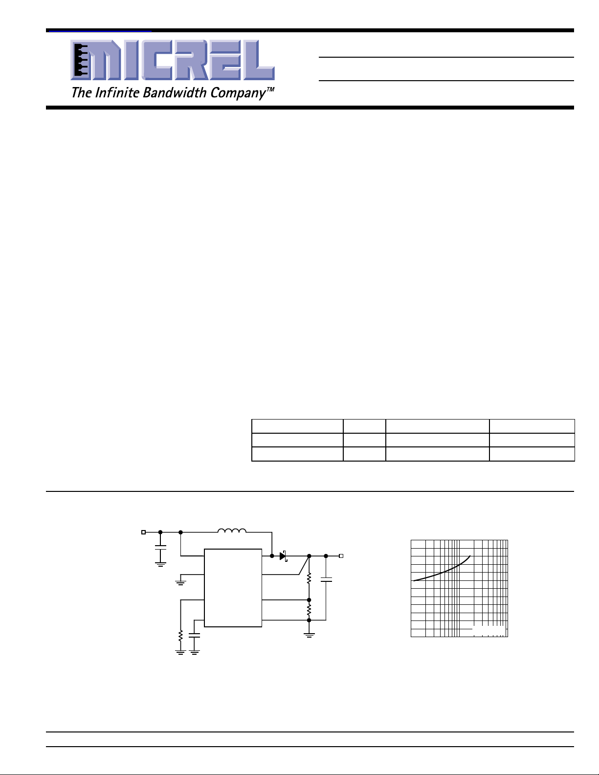
T ypical Application
V
3.0V to 5.0V
IN
C
IN
10 F/6.3V
Adjustable Output Boost Converter with Programmable Peak Switch Current
I Limit
Part Number Voltage Ambient Temp. Range Package
MIC2145BMM Adj –40°C to +85°C 8-lead MSOP
MIC2145BML Adj –40°C to +85°C3×3 MLF™-10L
L1
10 H
15
EN SW
4
PGND
MIC2145BMM
3
RSET
2
SS
VDD
SGND
FB
D1
6
7
8
V
OUT
10V/150mA
C
OUT
10 F/16V
10V Output
90
85
80
75
70
EFFICIENCY (%)
65
60
10 100 1000
Efficienc
VIN = 3.0V
OUTPUT CURRENT (mA)
Micrel, Inc. • 1849 Fortune Drive • San Jose, CA 95131 • USA • tel + 1 (408) 944-0800 • fax + 1 (408) 944-0970 • http://www.micrel.com
May 2003 1 MIC2145
MIC2145 Micrel
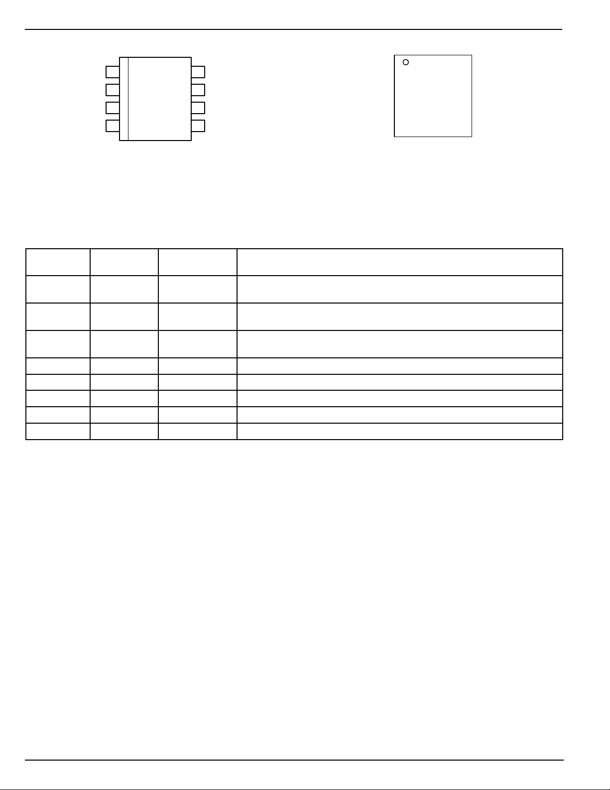
Pin Configuration
SS
RSET
PGND
1EN
2
3
4
8 SGND
FB
7
VDD
6
SW
5
8-Lead MSOP (MM)
Pin Description
Pin Number Pin Number Pin Name Pin Function
MSOP MLF
1 1 EN Enable (Input): Logic high (≥1.5V) enables regulator. Logic low (≤0.7V)
shuts down regulator. Do not float.
2 2 SS Soft Start Capacitor (External Component): Connect external capacitor to
ground to control the rise time of the output voltage.
3 3 RSET Current Limit (External Component): Sets peak current limit of the internal
power MOSFET using an external resistor.
4 4, 5 PGND Power Ground (Return): Internal power MOSFET source.
5 6, 7 SW Switch Node (Input): Internal power MOSFET drain.
6 8 VDD Supply (Input): +2.4V to +16V for internal circuitry.
7 9 FB Feedback (Input): Output voltage sense node.
8 10 SGND Small Signal Ground (Return): Ground
EN
1
SS
2
RSET
PGND
PGND SW
3
4
56
××
3mm
×3mm MLF-10L (ML)
××
10
9
8
7
SGND
FB
VDD
SW
MIC2145 2 May 2003

MIC2145 Micrel
Absolute Maximum Ratings (Note 1)
Supply Voltage (V
Switch Voltage (V
Feedback Voltage (V
Switch Current (ISW) ........................................................2A
Enable Voltage(V
RSET Voltage (V
ESD Rating, Note 3 ......................................................2kV
Ambient Storage Temperature(T
) ....................................................18V
DD
) ....................................................18V
SW
) ................................................18V
FB
), Note 5 ........................................18V
EN
)....................................................6V
RSET
) ..........–65°C to +150°C
S
Operating Ratings (Note 2)
Supply Voltage (V
Switch Voltage (V
Ambient Temperature (T
Junction Temperature (TJ) ....................... –40°C to +125°C
Package Thermal Resistance MSOP
(MSOP-8) ....................................................206°C/W
θ
JA
θJA (3mm×3mm MLF-10) ....................................60°C/W
) ....................................... 2.4V to 16V
DD
)....................................................16V
SW
)......................... –40°C to +85°C
A
Electrical Characteristics (Note 6)
VDD = 10V, V
Parameter Condition Min Typ Max Units
Supply Voltage 2.4 16 V
Shutdown Current EN = 0.3V, VDD = 10V, VFB=1.35V 0.5 5 µA
Quiescent Current EN = VDD, VDD = 10V, VFB = 1.35V 200 300 µA
Feedback Voltage Reference (±2%) 1.058 1.08 1.102 V
Comparator Hysteresis 18 mV
Feedback Input Current VFB=1.35V 40 nA
Peak Current Limit R
Current Limit Comparator 500 ns
Propagation Delay
Switch On-Resistance ISW = 150mA, VDD = 3.0V 500 750 mΩ
Maximum Off Time 1000 ns
Enable Input Voltage Logic Low (turn-off) 1.1 0.7 V
Enable Input Current VEN = 0V –1 0.01 1 µA
Soft Start Current VEN = 2V, VDD=3.0V –8 –12 –16 µA
OUT
= 10V, I
= 100mA; TJ =25°C, unless otherwise noted, bold values indicate –40°C ≤ TJ ≤ 125°C.
OUT
(±3%) 1.048 1.112 V
=200Ω, VDD = 3.6V, Note 4 0.8 A
SET
R
=1kΩ, VDD = 10V, Note 4 0.9 A
SET
ISW = 1.2A, VDD = 10V 250 400 mΩ
Logic High (turn-on) 1.5 1.1 V
VEN = 2V –1 0.01 1 µA
Note 1. Exceeding the absolute maximum rating may damage the device.
Note 2. The device is not guaranteed to function outside its operating rating.
Note 3. Devices are ESD sensitive. Handling precautions recommended. Human body model, 1.5KΩ in series with 100pF.
Note 4. The current is measured in a DC mode. Actual peak switching current will be higher due to internal propagation delay of the circuit.
Note 5. VEN ≤ VDD.
Note 6. Specification for packaged product only.
May 2003 3 MIC2145
MIC2145 Micrel
)
)
)
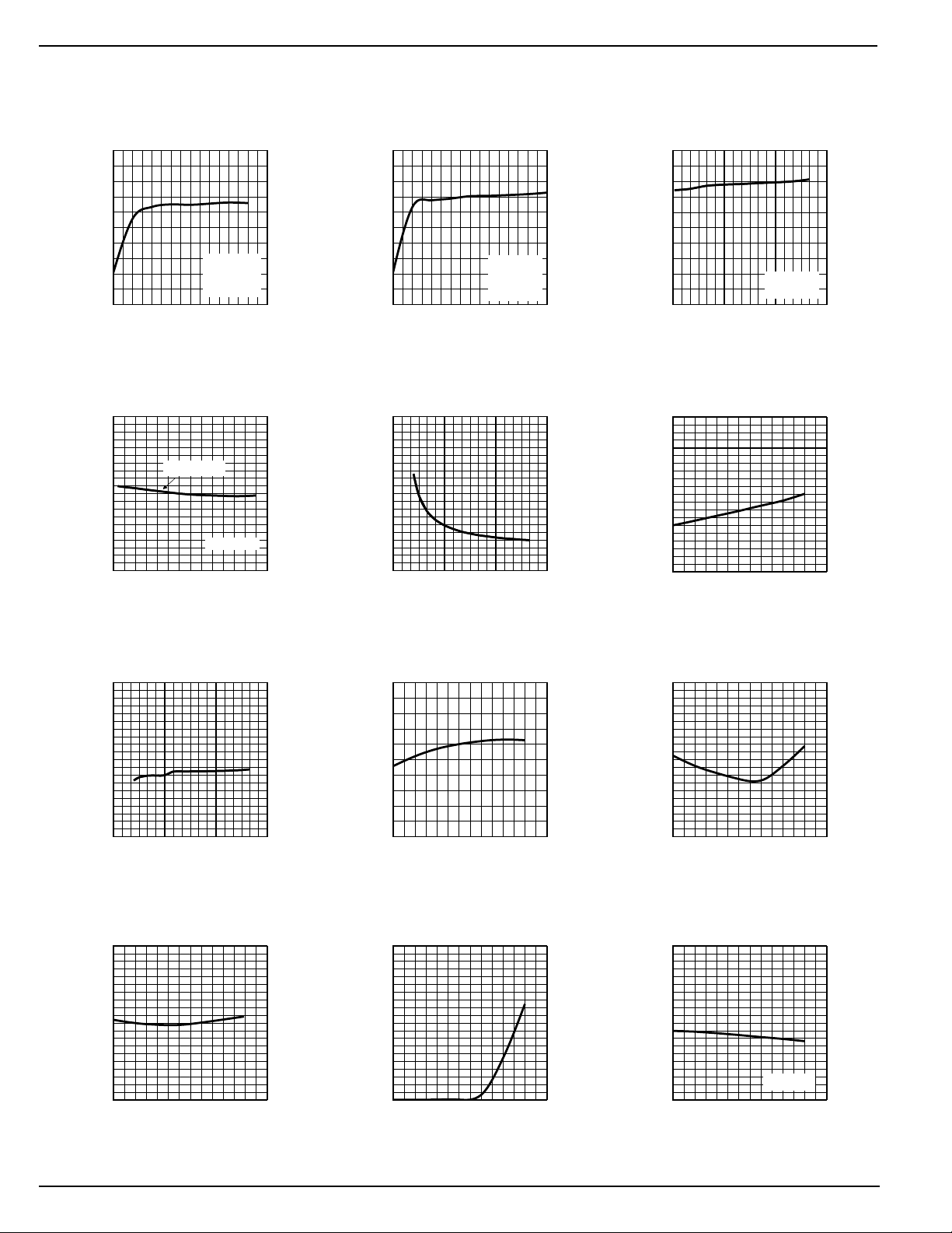
Typical Characteristics
Efficiency-Basic
100
90
80
70
EFFICIENCY (%)
60
50
16.0
15.8
15.6
15.4
15.2
(V)
15.0
OUT
14.8
V
14.6
14.4
14.2
14.0
Configuration
VIN = 3.3V
V
OUT
L = 10µH
0
0.01
0.02
0.03
0.04
OUTPUT CURRENT (A
0.05
Line Regulation
I
= 10mA
OUT
L = 10µH
246810121416
VDD (V)
= 10V
0.06
0.07
0.08
Efficiency-Bootstrapped
100
90
80
70
EFFICIENCY (%)
60
50
Configuration
0
0.01
0.02
0.03
OUTPUT CURRENT (A
0.04
V
V
L
IN
OUT
=
0.05
Switch On-Resistance
vs. V
1.0
0.9
0.8
0.7
0.6
0.5
0.4
0.3
0.2
0.1
SWITCH ON-RESISTANCE (Ω)
0.0
0 2 4 6 8 10 12 14 16 18
DD
VDD (V)
3.3V
=
=
10µH
0.06
10V
0.07
0.08
Load Regulation
9.8
9.6
9.4
9.2
0
0.01
0.02
OUTPUT CURRENT (A
0.03
0.04
VIN = 3.6V
L = 10µH
0.05
(V)
OUT
V
10.2
10.0
Switch On-Resistance
1.0
0.9
0.8
0.7
0.6
0.5
0.4
0.3
0.2
0.1
SWITCH ON-RESISTANCE (Ω)
0.0
vs. Temperature
-40 -20 0 20 40 60 80 100
TEMPERATURE (°C)
0.06
0.07
0.08
0.09
Quiescent Current
vs. V
0.50
0.45
0.40
0.35
0.30
0.25
0.20
0.15
0.10
0.05
QUIESCENT CURRENT (Ω)
0.00
0 2 4 6 8 10 12 14 16 18
1.5
1.4
1.3
1.2
1.1
1.0
0.9
0.8
OFF TIME (µs)
0.7
0.6
0.5
vs. Temperature
-40 -20 0 20 40 60 80 100
TEMPERATURE (°C)
DD
VDD (V)
Off Time
Feedback Voltage
1.1
1.09
1.08
1.07
1.06
FEEDBACK VOLTAGE (V)
1.05
vs. Temperature
-40 -20 0 20 40 60 80 100
TEMPERATURE (°C)
Shutdown Current
vs. Temperature
-40 -20 0 20 40 60 80 100
TEMPERATURE (°C)
SHUTDOWN CURRENT (µA)
0.50
0.45
0.40
0.35
0.30
0.25
0.20
0.15
0.10
0.05
0.00
Feedback Current
vs. Temperature
-40 -20 0 20 40 60 80 100
TEMPERATURE (°C)
FEEDBACK CURRENT (µA)
0.10
0.09
0.08
0.07
0.06
0.05
0.04
0.03
0.02
0.01
0.00
Quiescent Current
0.50
0.45
0.40
0.35
0.30
0.25
0.20
0.15
0.10
0.05
QUIESCENT CURRENT (mA)
0.00
vs. Temperature
VIN = 3.6V
-40 -20 0 20 40 60 80 100
TEMPERATURE (°C)
MIC2145 4 May 2003
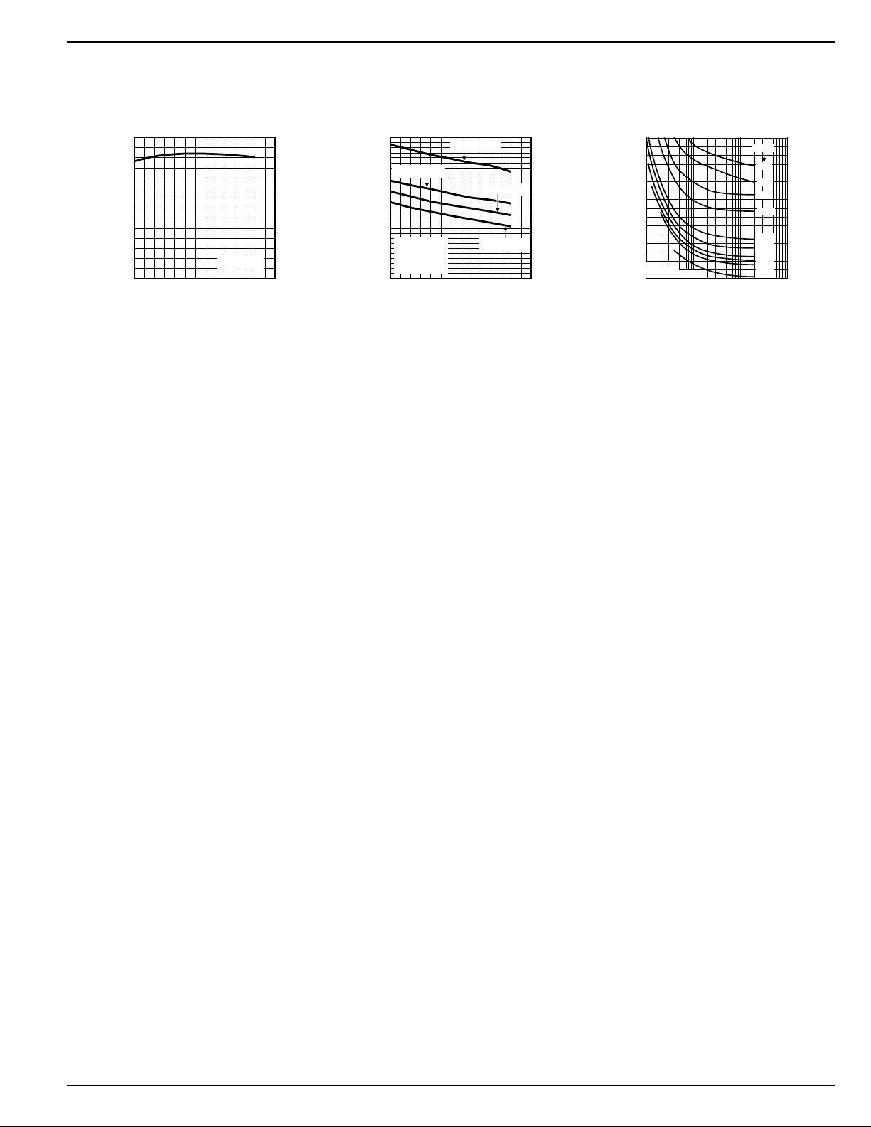
MIC2145 Micrel
400
600
800
1000
1200
1400
1600
1800
2000
100 1000 10000 100000
PEAK CURRENT LIMIT (mA)
RSET(Ω)
Peak Current Limit
vs. RSET
15V
5.0V
4.2V
2.4V
3.0V
3.3V
3.6V
8.0V
10V
12V
VOUT/VIN > 1.25
L = 10µH
VIN =
Soft Start Current
vs. Temperature
14
12
10
8
6
4
2
SOFT START CURRENT (µA)
0
-40 -20 0 20 40 60 80 100
TEMPERATURE (°C)
VIN = 3.6V
Peak Current Limit
1.4
1.3
1.2
1.1
1.0
0.9
0.8
0.7
0.6
0.5
0.4
0.3
0.2
PEAK CURRENT LIMIT (A)
0.1
vs. Temperature
R
= 200
SET
R
= 500
SET
VIN = 3.6V
V
= 10V
OUT
L = 10µH
0
-40 -20 0 20 40 60 80 100
R
SET
R
= 10k
SET
TEMPERATURE (°C)
= 1k
May 2003 5 MIC2145
 Loading...