

MIC2142 Micrel
查询MIC2142供应商
MIC2142
Micropower Boost Converter
Preliminary Information
General Description
The MIC2142 is a micropower boost switching regulator
housed in a SOT23-5 package. The input voltage range is
between 2.2V to 16V, making the device suitable for one-cell
Li Ion and 3 to 4-cell alkaline/NiCad/NiMH applications. The
output voltage of the MIC2142 can be adjusted up to 22V.
The MIC2142 is well suited for portable, space-sensitive
applications. It features a low quiescent current of 85µA, and
a typical shutdown current of 0.1µA. It’s 330kHz operation
allows small surface mount external components to be used.
The MIC2142 is capable of efficiences over 85% in a small
board area.
The MIC2142 can be configured to efficiently power a variety
of loads. It is capable of providing a few mA output for
supplying low power bias voltages; it is also capable of
providing the 80mA needed to drive 4 white LEDs.
The MIC2142 is available in a SOT23-5 package with an
ambient operating temperature range from –40°C to +85°C
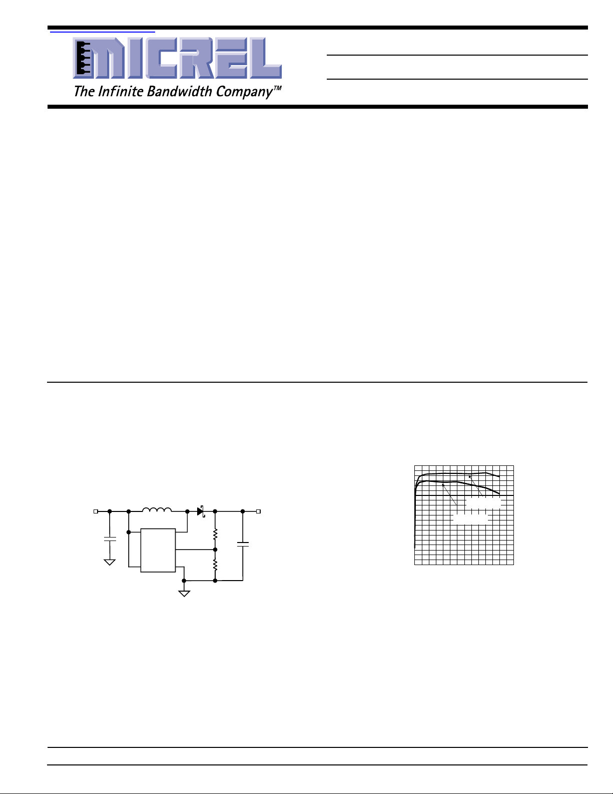
Typical Application
Features
• 2.2V to 16V input voltage
• Up to 22V output voltage
• 330kHz switching frequency
• 0.1µA shutdown current
•85µA quiescent current
• Implements low-power boost, SEPIC, or flyback
• SOT23-5 package
Applications
• LCD bias supply
• White LED driver
• 12V Flash memory supply
• Local 3V to 5V conversion
2.8V to 4.7V
V
IN
C
IN
10µF
L1
33µH
MIC2142
VCC SW
1
5
FB
GNDEN
D1
3
4
2
R2
365k
R1
124k
Typical Configuration
+5V @60mA
C
OUT
22µF
Efficiency
vs. Output Current
0.90
0.85
0.80
0.75
0.70
0.65
0.60
0.55
EFFICIENCY (%)
0.50
0.45
0.40
0 10203040506070
OUTPUT CURRENT (mA)
VIN = 4.2V
VIN = 3.0V
Efficiency vs. Output Current
Micrel, Inc. • 1849 Fortune Drive • San Jose, CA 95131 • USA • tel + 1 (408) 944-0800 • fax + 1 (408) 944-0970 • http://www.micrel.com
December 2000 1 MIC2142
MIC2142 Micrel
Ordering Information
Part Number Voltage Ambient Temp. Range Package
MIC2142BM5 Adj –40°C to +85°C SOT23-5
Pin Configuration
VCC
GND
SW
13
2
SBAA
45
FB
SOT23-5 (BM5)
EN
Part
Identification
Pin Description
Pin Number Pin Name Pin Function
1 VCC Chip Supply: +2.2V to +16V
2 GND Ground: Return for internal circuitry and internal MOSFET (switch) source.
3 SW Switch Node (Input): Internal MOSFET drain; 22V maximum.
4 FB Feedback (Input): Output voltage sense node.
5 EN Shutdown: Device shuts down to 0.1µA typical supply current.
MIC2142 2 December 2000
MIC2142 Micrel
Absolute Maximum Ratings (Note 1)
Supply voltage (VCC).....................................................18V
Switch voltage (V
Enable pin voltage (V
Feedback Voltage (VFB)
Adjustable version.......................................................8V
Ambient Storage Temperature (TS) .........–65°C to +150°C
) ....................................................24V
SW
) Note 3...................................18V
EN
Operating Ratings (Note 2)
Supply Voltage (VCC) ....................................... 2.2V to 16V
Enable pin voltage (V
Switch Voltage (V
Ambient Temperature (TA).........................–40°C to +85°C
Junction Temperature Range (T
Package Thermal Impedance
θ
SOT23-5 .....................................................220°C/W
JA
) Note 3......................... 0V to 16V
EN
)....................................................22V
SW
) ...........–40°C to +125°C
J
Electrical Characteristics
VCC =3.6V, V
Parameter Condition Min Typ Max Units
Input Voltage 2.2 16 V
Quiescent Current VEN = ON , VFB = 2.2V 85 125 µA
Feedback Voltage (VFB)(±2%) 1.254 1.28 1.306 V
Comparator Hysteresis 18 mV
Feedback Input Bias Current 30 nA
Note 4
Enable Input Voltage VIH (turn on) 0.6VCC0.55V
Enable Input Current –1 0.01 1 µA
Load Regulation 200µA ≤ I
Line Regulation 2.2V ≤ VCC ≤ 16V; I
SW on Resistance ISW = 100mA, VCC = 2.5V 5 Ω
Switch Leakage Current VEN = OFF, VSW = 12V 0.05 1 µA
Oscillator Frequency 295 330 365 kHz
Duty Cycle 50 57 65 %
OUT
= 5V, I
= 20mA, TA=25°C; unless otherwise specified. Bold values indicate 25°C ≤ TJ ≤ 125°C.
OUT
VEN = OFF (shutdown) 0.1 2 µA
(±3%) 1.241 1.312 V
VIL (turn off) 1.1 0.8 V
≤ 20mA 0.2 %V
OUT
= 4mA 0.25 %/V
OUT
ISW = 100mA, VCC = 12V 2 Ω
CC
V
OUT
Note 1: Absolute maximum ratings indicate limits beyond which damage to the component may occur. Electrical specifications do not apply when
Note 2: The device is not guaranteed to function outside its operating rating.
Note 3: VEN must be ≤ V
Note 4: The maximum suggested value of the programming resistor, whose series resistance is measured from feedback to ground, is 124kΩ. Use of
Note 5: Devices are ESD sensitive, handling precautions required.
operating the device outside of its operating ratings. The maximum allowable power dissipation is a function of the maximum junction
temperature, T
dissipation will result in excessive die temperature, and the regulator will go into thermal shutdown. The θJA of the power SOT23-5 is 220°C/W
mounted on a PC board.
larger resistor values can cause errors in the output voltage due to the feedback input bias current.
, the junction-to-ambient thermal resistance, θJA, and the ambient temperature, TA. The maximum allowable power
J(Max)
IN
December 2000 3 MIC2142
MIC2142 Micrel
µ
g
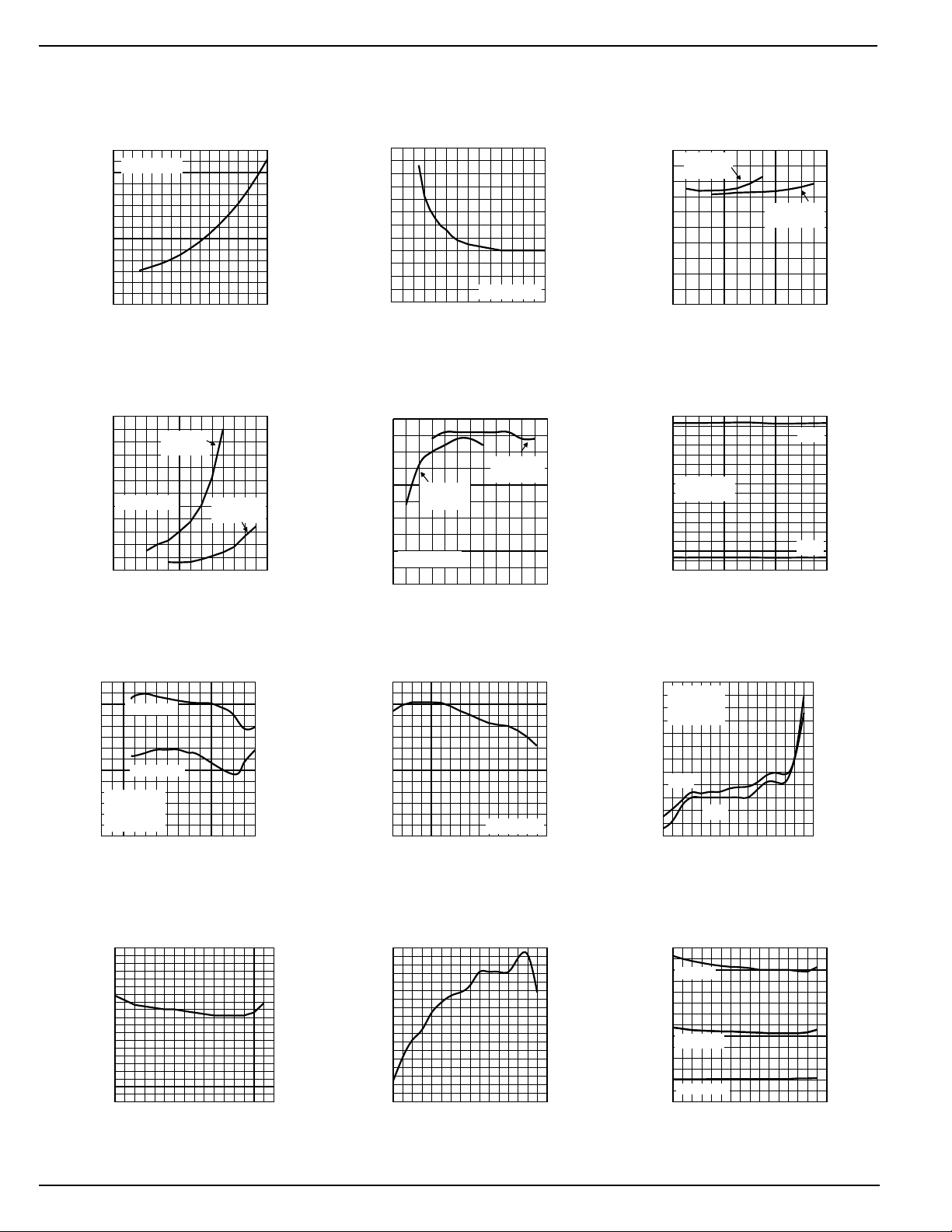
Typical Characteristics
Quiescent Current
vs. Input Voltage
350
V
= 5V
OUT
300
250
200
150
100
50
QUIESCENT CURENT (µA)
0
0 2 4 6 8 10 12 14 16
INPUT VOLTAGE (V)
Output Ripple
1200
1000
OUTPUT RIPPLE (mV)
vs. Input Voltage
IL = 7mA
L = 22
H
800
600
V
= 15V
OUT
400
200
0
02468101214
INPUT VOLTAGE (V)
IL = 2mA
L = 220µH
VDS and R
vs. Input Voltage
600
500
400
(V)
300
DS
V
200
100
0
0 2 4 6 8 10 12 14
INPUT VOLTAGE (V)
DS(ON)
ISW= 100mA
Efficiency
vs. Input Voltage
85
80
75
IL = 7mA
L = 22µH
70
EFFICIENCY (%)
65
V
= 15V
OUT
60
2 4 6 8 101214
INPUT VOLTAGE (V)
IL = 2mA
L = 220µH
6
5
4
3
DS(ON)
R
2
1
0
16.5
15.5
14.5
OUTPUT VOLTAGE (V)
OUTPUT VOLTAGE (V)
Line Regulation
I
= 7mA
L
L = 22µH
16
IL= 2mA
L = 220µH
15
14
2 4 6 8 10 12 14
INPUT VOLTAGE (V)
MIC2142 Load
ulation
16
14
12
10
8
6
4
2
0
0 5 10 15 20 25 30
Re
L = 22µH
VIN = 5V
OUTPUT CURRENT (mA)
V
V
OUT
REF
Oscillator Characteristics
350
300
250
200
150
100
FREQUENCY (kHz)
vs. Input Voltage
Frequency
Duty Cycle
VO = 15V
I
= 100µA
O
50
L= 220µH
0
02468101214
INPUT VOLTAGE (V)
tON vs.
2
1.9
1.8
1.7
1.6
1.5
(µsec)
1.4
ON
t
1.3
1.2
1.1
1
-50 -30 -10 10 30 50 70 90 110
Temperature
TEMPERATURE (°C)
0.65
0.60
0.55
0.50
0.45
0.40
DUTY CYCLE
Quiescent Current
vs. Temperature
84
82
80
78
76
74
72
QUIESCENT CURRENT (µA)
70
-50 -30 -10 10 30 50 70 90 110
TEMPERATURE (°C)
Frequency vs.
340
335
330
325
320
315
310
305
FREQUENCY (kHz)
300
295
-50 -30 -10 10 30 50 70 90 110
Temperature
TEMPERATURE (°C)
VIN = 3.6V
V
and V
OUT
15.20
15.15
15.10
15.05
15.00
14.95
OUTPUT VOLTAGE (V)
14.90
Over Temperature
V
=
3.6V
IN
I
= 100µA
O
L = 22µH
V
OUT
V
REF
-50 -30 -10 10 30 50 70 90 110
TEMPERATURE (°C)
Timing Characteristics
Over Temperature
3.5
3.0
T (µsec)
2.5
2.0
1.5
tON (µsec)
1.0
0.5
Duty Cycle
0
OSCILLATOR CHARACTERISTICS
-50 -30 -10 10 30 50 70 90 110
TEMPERATURE (°C)
REF
1.290
1.285
1.280
1.275
REFERENCE VOLTAGE (V)
1.270
MIC2142 4 December 2000
MIC2142 Micrel
R
vs.
DS(ON)
Temperature
7
6
5
(Ω)
4
3
DS(ON)
R
2
1
0
-50 -30 -10 10 30 50 70 90 110
VCC=3.3V
VCC = 4.5V
TEMPERATURE (°C)
Timing Characteristics
Over Temperature
0.6
0.58
0.56
0.54
0.52
0.5
0.48
0.46
DUTY CYCLE (%)
0.44
0.42
0.4
-50 -30 -10 10 30 50 70 90 110
TEMPERATURE (°C)
December 2000 5 MIC2142
MIC2142 Micrel
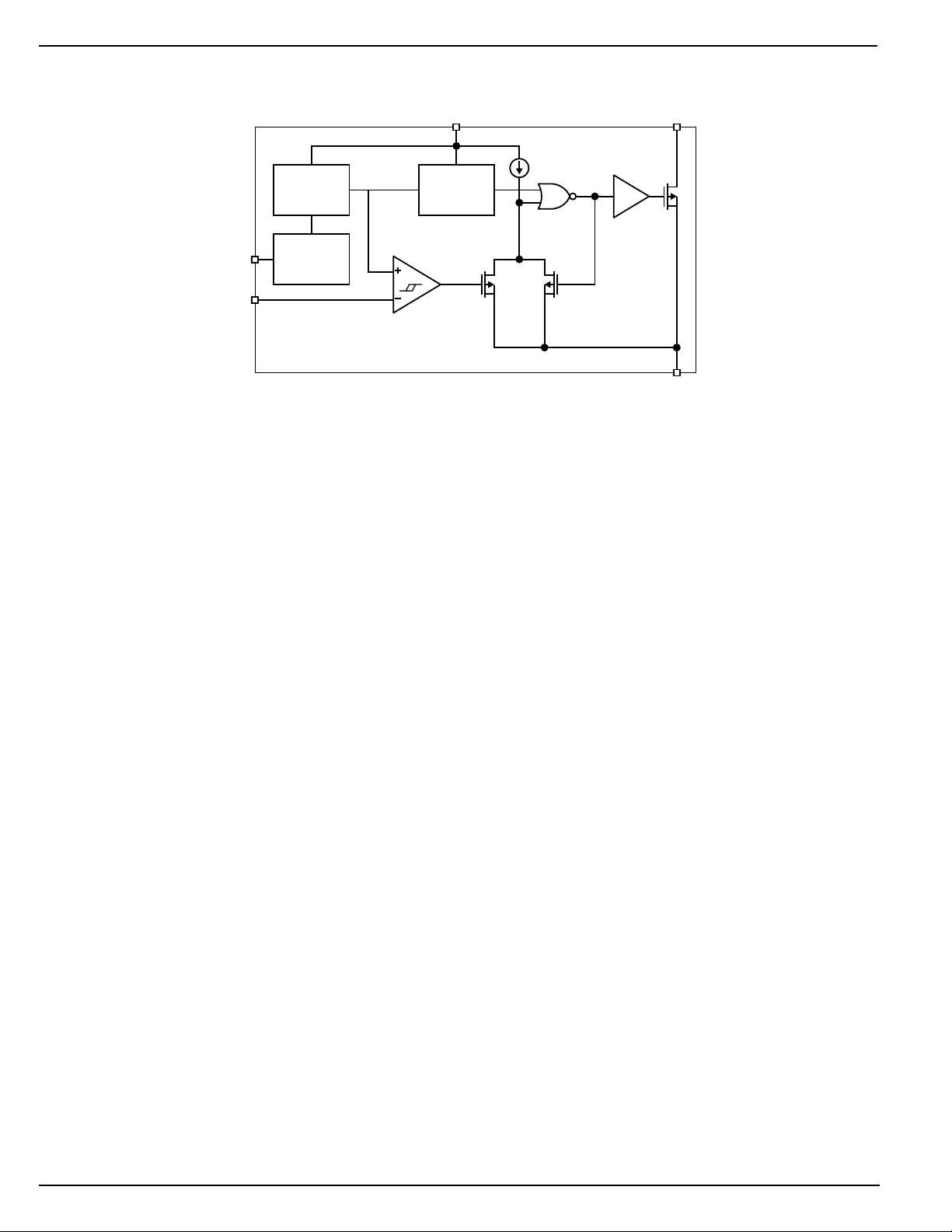
Functional Diagram
EN
FB
Bandgap
Reference
Shutdown
MIC2142
VCC
Oscillator
330kHz
FIXED DUTY CYCLE
SW
GND
Functional Description
This MIC2142 is a fixed duty cycle, constant frequency, gated
oscillator, micropower, switch-mode power supply controller.
Quiescent current for the MIC2142 is only 85µA in the switch
off state, and since a MOSFET output switch is used, additional switch drive current is minimized. Efficiencies above
85% throughout most operating conditions can be realized.
A functional block diagram is shown above and typical
schematic is shown on page 1. Regulation is performed by a
hysteretic comparator, which regulates the output voltage by
gating the internal oscillator. The internal oscillator operates
at a fixed 57% duty cycle and 330kHz frequency. For the fixed
output versions, the output is divided down internally and then
compared to the internal V
divider is use for the adjustable version.
The comparator has hysteresis built into it, which determines
the amount of low frequency ripple that will be present on the
input. An external resistive
REF
output. Once the feedback input to the comparator exceeds
the control voltage by 18mV, the high frequency oscillator
drive is removed from the output switch. As the feedback
input to the comparator returns to the reference voltage level,
the comparator is reset and the high frequency oscillator is
again gated to the output switch. The 18mV of hysteresis
seen at the comparator will be multiplied by the ratio of the
output voltage to the reference voltage. For a five volt output
this ratio would be 4, corresponding to a ripple voltage of
72mV at the output.
The maximum output voltage is limited by the voltage capability of the output switch. Output voltages up to 22V can be
achieved with a standard boost circuit. Higher output voltages can be realized with a flyback configuration.
MIC2142 6 December 2000

MIC2142 Micrel
Application Information
Predesigned circuit information is at the end of this section.
Component Selection
Resistive Divider (Adjustable Version)
The external resistive divider should divide the output voltage
down to the nominal reference voltage. Current drawn through
this resistor string should be limited in order to limit the effect
on the overall efficiency. The maximum value of the resistor
string is limited by the feedback input bias current and the
potential for noise being coupled into the feedback pin. A
resistor string on the order of 2MΩ limits the additional load
on the output to 20µA for a 20V output. In addition, the
feedback input bias current error would add a nominal 60mV
error to the expected output. Equation 1 can be used for
determining the values for R2 and R1.
R1 R2
+
(1)
V
OUT
=
Boost Inductor
Maximum power is delivered to the load when the oscillator
is gated on 100% of the time. Total output power and circuit
efficiency must be considered when determining the maximum inductor value. The largest inductor possible is preferable in order to minimize the peak current and output ripple.
Efficiency can vary from 80% to 90% depending upon input
voltage, output voltage, load current, inductor, and output
diode.
Equation 2 solves for the output current capability for a given
inductor value and expected efficiency. Figures 7 through 12
show estimates for maximum output current assuming the
minimum duty and maximum frequency and 80% efficiency.
To determine the necessary inductance, find the intersection
between the output voltage and current, and then select the
value of the inductor curve just above the intersection. If the
efficiency is expected to be different than the 85% used for the
graph, Equation 2 can then be used to better determine the
maximum output capability.
The peak inductor/switch current can be calculated from
Equation 3 or read from the graph in Figure 13. The peak
current shown in the graph in Figure 13 is derived assuming
a max duty cycle and a minimum frequency. The selected
inductor and diode peak current capability must be greater
than this. The peak current seen by the inductor is calculated
at the maximum input voltage. A wide ranging input voltage
will result in a higher worst case peak current in the inductor
than a narrow input range.
()
=
tV
ON max IN max
()()
=
(2)
(3)
I
O(max)
I
PK
Table 1 lists common inductors suitable for most applications. Due to the internal transistor peak current limitation at
low input voltages, inductor values less than 10µH are not
V
REF
R1
Vt
IN(min)
2L T
MAX
L
MIN
2
ON
S
V
eff
1
O
V
−
IN min
()
×
recommmended. Table 6 lists minimum inductor sizes versus
input and output voltage. In low-cost, low-peak-current applications, RF-type leaded inductors may sufficient. All inductors listed in Table 5 can be found within the selection of
CR32- or LQH4C-series inductors from either Sumida or
muRata.
rerutcafunaMseireSepyTeciveD
ataRuMC4/C3/C1HQLtnuomecafrus
adimuS23RCtnuomecafrus
relliM.W.JF87dedaellaixa
tfarclioC09dedaellaixa
Table 1. Inductor Examples
Boost Output Diode
Speed, forward voltage, and reverse current are very important in selecting the output diode. In the boost configuration
the average diode current is the same as the average load
current and the peak is the same as the inductor and switch
current. The peak current is the same as the peak inductor
current and can be derived from Equation 3 or the graph in
Figure 13. Care must be taken to make sure that the peak
current is evaluated at the maximum input voltage.
The BAT54 and BAT85 series are low current Shottky diodes
available from “On Semiconductor” and “Phillips” respectively. They are suitable for peak repetitive currents of 300mA
or less with good reverse current characteristics. For applications that are cost driven, the 1N4148 or equivalent will
provide sufficient switching speed with greater forward drop
and reduced cost. Other acceptable diodes are On
Semiconductor’s MBR0530 or Vishay’s B0530, although
they can have reverse currents that exceed 1 mA at very high
junction temperatures. Table 2 summarizes some typical
performance characteristics of various suitable diodes.
57C°
V
edoiD
0350RBMV572.0V523.0Aµ5.2Aµ09
8414N1
45TAB
58TAB
DWF
ta
Am001
V6.0
V4.0
45.0
C°52
V
DWF
ta
Am001
V59.0
)C°571(
)C°58(
)C°58(
V54.0
V65.0Aµ4.0
mooR
.pmeT
egakaeL
V51ta
An52
)V02(
An01
)V52(
C°57
egakaeL
V51ta
Aµ2.0
)V02(
Aµ1
)V02(
Aµ2
)C5°8(
egakcaP
321DOS
TMS
dedael
TMSdna
TMS
43-OD
dedael
Table 2. Diode Examples
Output Capacitor
Due to the limited availability of tantalum capacitors, ceramic
capacitors and inexpensive electrolyics may be preferred.
Selection of the capacitor value will depend upon the peak
inductor current and inductor size. MuRata offers the GRM
series with up to 10uF @ 25V with a Y5V temperature
coefficient in a 1210 surface mount package. Low cost
applications can use the M series leaded electrolytic capacitor from Panasonic. In general, ceramic, electrolytic, or
tantalum values ranging from 1µF to 22µF can be used for the
output capacitor.
December 2000 7 MIC2142

MIC2142 Micrel
rerutcafunaMseireSepyTegakcaP
ataRuMMRGV5Ycimarectnuomecafrus
yahsiV495mulatnattnuomecafrus
cinosanaPseires-Mcitylortcelededael
Table 3. Capacitor Examples
Design Example
Given a design requirement of 12V output and 1mA load with
an miniumum input voltage of 2.5V, Equation 2 can be used
to calculate to maximum inductance or it can be read from the
graph in Figure 7. Once the maximum inductance has been
determined the peak current can be determined using Equation 3 or the graph in Figure 13.
V
= 12V
OUT
I
= 5mA
OUT
VIN = 2.5V to 4.7V
F
= 360kHz
max
η = 0.8 = efficiency
D
= 0.55
nom
T
S(min)
t
ON(min)
L
max
L
max
1
== =µ
F
max
D
nom
== µ
f
max
Vt
IN(min)
=
I2T
O(max) S(min)
2
25 153
..
=
52278
mA
×× µ
1
360kHz
0.55
360kHz
22
×
ON(min)
××
2.78 sec
1.53 sec
×
V
O
η
2
×µ
sec
×
12
sec
.
08
.
−
1
−
1
V
IN(min)
25
.
H
42
=µ
Bootstrap Configuration
For input voltages below 4.5V the bootstrap configuration can
increase the output power capability of the MIC2142. Figure
2 shows the bootstrap configuration where the output voltage
is used to bias the MIC2142. This impoves the power capability of the MIC2142 by increasing the gate drive voltage
hence the peak current capability of the internal switch. This
allows the use of a smaller inductor which increases the
output power capability. Table 4 also summarizes the various
configurations and power capabilities using the booststrap
configuration. This bootstrap configuration is limited to output
voltage of 16V or less.
Figure 1 shows how a resistor (R3) can be added to reduce
the ripple seen at the V
pin when in the bootstrap configu-
CC
ration. Reducing the ripple at the VCC pin can improve output
ripple in some applications.
+3.0V to +4.2V
V
IN
C2
10µF
L1
33µH
U1 MIC2142
FB SW
4
5
GND
VCCEN
CR1
MBR0530
3
2
1
100
C4
1µF
R3
R2
36.5k
R1
12.4k
C1
22µF
+5V @80mA
C3
270pF
GNDGND
Figure 1. Bootstrap VCC with VCC Low Pass Filter
Select 39µH ±10%.
t
ON(max)
I
peak
1.1 D
=
tV
ON(max)
=
F
×
L
min
min
nom
×
1.1 0.55
=
IN(max)
×
300kHz
µ×
2.0 sec 4.7V
=
35 H
=µ
2 sec
µ
=
270mA
MIC2142 8 December 2000
MIC2142 Micrel
L1
V
IN
47µH
CR1
MBR0530
+5V @16mA
For additional predesigned circuits, see Table 4.
V
C2
10µF
U1 MIC2142
FB SW
4
GND
VCCEN
5
3
2
1
Figure 2. Booststrap Configuration
L1
10µH
IN
CR1
MBR0530
R2
36.5k
R1
12.4k
C1
22µF
C3
270pF
GNDGND
CR5
LWT673
CR7
LWT673
+15V @15mA
(from µcontroller)
PWM
C2
10µF
U1 MIC2142
FB SW
4
GND
VCCEN
5
3
2
1
C1
1µF
25V
Rprogram
82Ω
CR6
LWT673
GNDGND
Figure 3. Series White LED Driver with PWM Dimming Control
V
SHTDWN
L1
10µH
IN
U1 MIC2142
FB SW
4
10µF
C2
GND
VCCEN
5
CR1
MBR0530
3
2
1
C1
1µF
25V
CR5
LWT673
CR7
LWT673
CR6
LWT673
Rprogram
82Ω
+15V @15mA
GNDGND
DAC
R4 R3
Figure 4. Series White LED Driver with Analog Dimming Control
December 2000 9 MIC2142

MIC2142 Micrel
L1
V
IN
10µH
CR3
MBR0530
+5.0V @50mA
EN
GND
DAC
C2
10µF
R4 R3
U1 MIC2142
FB SW
4
GND
VCC EN
5
3
2
1
C1
1µF
25V
CR1
LWT673
R1
120Ω
CR2
LWT673
R2
120Ω
Figure 5. Parallel White LED Driver with Analog Dimming Control
V
IN
C2
10µF
L1
10µH
U1 MIC2142
FB SW
4
5
GND
VCCEN
CR1
BAT54HT1
3
2
1
C1
1µF
25V
R2
1.8M
R1
120k
+20V @0.5mA
C1
1µF
25V
CR3
LWT673
R3
120Ω
GND
INRTN
GNDV
Figure 6. Handheld LCD Supply
MIC2142 10 December 2000

MIC2142 Micrel
Predesigned Circuit Values
V
IN(min)
V
IN(max)
V
OUT
I
OUT(max)
L1 IPK @ V
IN(max)
CR1
2.5V 3.0V 3.3V 40mA 47µH 129mA BAT54
23mA 85µH 74mA BAT54
10mA 180µH 34VmA BAT54
2.5V 4.5V 5V 16.5mA 47µH 193mA BAT54
7.8mA 100µH 91mA BAT54
boot strapped 51 15 605 MBR0530
boot strapped 77 10 908 MBR
2.5 11.5 12 4.8 47 493 MBR
2.25 100 232 BAT
4.7 boot strapped 15 15 632 MBR
boot strapped 22 10 950 MBR
2.5 14.5 15 3.7 47 622 MBR
1.7 100 292 BAT
4.7 boot strapped 17.4 10 950 MBR
boot strapped 8 22 430 MBR
2.5 4.7 20 2.7 47 202 BAT
2.5 4.7 20 1.5 82 110 BAT
3.0 4.7 5 40 33 287 BAT
boot strapped 70 18 525 MBR
boot strapped 100 12 800 MBR
3.0 8.5 9 15 33 520 MBR
4.7 boot strapped 28 18 525 MBR
4.7 boot strapped 40 12 800 MBR
3.0 14.5 15 7.8 33 886 MBR
3.0 4.7 boot strapped 14 18 525 MBR
3.0 4.7 boot strapped 21 12 800 MBR
3.0 4.7 20 5.6 33 287 BAT
5.0 8.5 9 70 27 635 MBR
23 82 209 BAT
10 180 95 BAT
5.0 11.5 12 43 27 860 MBR
14 82 283 BAT
6 180 129 BAT
5.0 14.5 15 30 27 1083 MBR
10 82 357 MBR
9 30 27 672 MBR
5.0 8.0 20 8 68 237 BAT
9 11.5 12 118 56 414 MBR
66 100 232 BAT
30 220 105 BAT
9 14 15 70 56 504 MBR
40 100 282 BAT
18 220 128 BAT
9 14 20 20 120 235 BAT
10 220 128 BAT
6 390 72 BAT
12 14 15 156 68 415 MBR
71 150 182 BAT
27 390 72 BAT
12 14 20 35 150 188 BAT
Table 4. Typical Maximum Power Configuration
December 2000 11 MIC2142

MIC2142 Micrel
V
NI
%5±V3.3V5
%5±V5V9
%5±V21V51
V
TUO
V9
V21
V51
V02
V21
V51
V02
V02
I
TUO
Am07
Am03
Am02
Am51
Am6
Am07
Am04
Am03
Am0.8
851
53
1L1RCI
Hµ81
Hµ81
Hµ81
Hµ81
Hµ33
Hµ72
Hµ72
Hµ72
Hµ86
86
051
0350RBM
0350RBM
0350RBM
0350RBM
45TAB
0350RBM
0350RBM
0350RBM
45TAB
0530RBM
45TAB
KAEP
004
004
004
004
partstooB
partstooB
partstooB
partstooB
412
073
073
073
841
053
061
%5±V51V020502245TAB0411
Table 5. Typical Maximum Power Configurations for Regulated Inputs
V
= 16V to 22V V
OUT
85C 85C 40C
VIN (V) L
2.5 47 47 (15) 47 (10)
3 33 33 (18) 33 (12)
3.5 47 27 (22) 27 (15)
4 56 27 (22) 22 (18)
568 27 22
682 33 22
7 100 39 27
8 100 47 33
9 120 56 33
10 150 56 39
11 150 68 47
12 150 68 47
13 180 82 56
14 180 82 56
15 220 82 56
16 220 100 68
(µH) L
MIN
< 16V (boostraped) V
OUT
(µH) L
MIN
< 16 (boostraped)
OUT
(µH)
MIN
Table 6. Minimum Inductance
noitarugifnoC
Manufacturer Web Address
MuRata www.MuRata.com
Sumida www.sumida.com
Coilcraft www.coilcraft.com
J. W. Miller www.jwmiller.com
Micrel www.micrel.com
Vishay www.vishay.com
Panasonic www.panasonic.com
Table 7. Component Supplier Websites
MIC2142 12 December 2000

MIC2142 Micrel
Inductor Selection Guides
1000
10µH
12µH
15µH
18µH
100
22µH
33µH
39µH
47µH
56µH
68µH
82µH
100µH
120µH
MAX. OUTPUT CURRENT (mA)
150µ
H
180µH
10
220µH
VIN = 2.5V
1000
12µH
15µH
18µH
22µH
27µH
33µH
39µH
100
47µH
56µH
68µH
82µH
100µH
120µH
150µH
180µH
220µH
MAX. OUTPUT CURRENT (mA)
10
VIN = 3.0V
1
0246810121416182022
OUTPUT VOLTAGE (V)
Figure 7. Inductor Selection for VIN = 2.5V
1
0 2 4 6 8 1012141618202224
OUTPUT VOLTAGE (V)
Figure 8. Inductor Selection for VIN = 3.0V
December 2000 13 MIC2142

MIC2142 Micrel
1000
18µH
22µH
27µH
33µH
39µH
47µH
56µH
68µH
82µH
100µH
100
120µH
150µH
180µH
220µH
MAX. OUTPUT CURRENT (mA)
10
VIN = 5.0V
1000
39µH
47µH
56µH
68µH
82µH
100µH
100
120µH
150µH
180µH
220µH
270µH
330µH
390µH
470µH
MAX. OUTPUT CURRENT (mA)
10
VIN = 9.0V
1
24681012141618202224
Figure 9. Inductor Selection for V
OUTPUT VOLTAGE (V)
IN
= 5V
1
8 1012141618202224
OUTPUT VOLTAGE (V)
Figure 10. Inductor Selection for VIN = 9V
MIC2142 14 December 2000

MIC2142 Micrel
)
1000
47µH
56µH
68µH
82µH
100µH
120µH
150µH
180µH
220µH
270µH
100
330µH
390µH
470µH
MAX. OUTPUT CURRENT (mA)
10
VIN = 12.0V
1000
100
MAX. OUTPUT CURRENT (mA)
VIN = 15V
56µH
68µH
82µH
100µH
120µH
150µH
180µH
1
10 12 14 16 18 20 22 24
OUTPUT VOLTAGE (V)
Figure 11. Inductor Selection for VIN = 12V
220µH
270µH
330µH
390µH
470µH
10
14 16 18 20 22 24
OUTPUT VOLTAGE (V
Figure 12. Inductor Selection for VIN = 15V
December 2000 15 MIC2142

MIC2142 Micrel
600
500
400
300
PEAK CURRENT (mA)
200
10µH
12µH
15µH
18µH
27µH
22µH
39µH
33µH
47µH
56µH
68µH
82µH
4.5V to 15VCC Limit
100µH
120µH
150µH
3.5VCC Limit
180µH
220µH
100
0
0 1 2 3 4 5 6 7 8 9 10111213141516171819202122
INPUT VOLTAGE (V)
Figure 13. Peak Inductor Current vs. Input Voltage
16V to 20VOUT Limit
8.2µH
2.5VCC Limit
MIC2142 16 December 2000

MIC2142 Micrel
Package Information
1.90 (0.075) REF
0.95 (0.037) REF
3.02 (0.119)
2.80 (0.110)
0.50 (0.020)
0.35 (0.014)
1.75 (0.069)
1.50 (0.059)
1.30 (0.051)
0.90 (0.035)
0.15 (0.006)
0.00 (0.000)
SOT23-5 (M3)
3.00 (0.118)
2.60 (0.102)
10°
0°
DIMENSIONS:
MM (INCH)
0.20 (0.008)
0.09 (0.004)
0.60 (0.024)
0.10 (0.004)
MICREL INC. 1849 FORTUNE DRIVE SAN JOSE, CA 95131 USA
TEL + 1 (408) 944-0800 FAX + 1 (408) 944-0970 WEB http://www.micrel.com
This information is believed to be accurate and reliable, however no responsibility is assumed by Micrel for its use nor for any infringement of patents or
other rights of third parties resulting from its use. No license is granted by implication or otherwise under any patent or patent right of Micrel Inc.
© 2000 Micrel Incorporated
December 2000 17 MIC2142
 Loading...