

Micrel MIC2141 User Manual
MIC2141 Micrel
查询MIC2141供应商
MIC2141
Micropower Boost Converter
Preliminary Information
General Description
The MIC2141 is a micropower boost switching regulator that
can operate from 3- or 4-cell nickel-metal-hydride batteries or
a single Li-ion cell. This regulator employs a constant 330kHz,
fixed 18% duty-cycle, gated-oscillator architecture.
The MIC2141 can be used in applications where the output
voltage must be dynamically adjusted. The device features a
control signal input which is used to proportionally adjust the
output voltage. The control signal input has a gain of 6,
allowing a 0.8V to 3.6V control signal to vary a 4.8V to 22V
output.
The MIC2141 requires only three external components to
operate and is available in a tiny 5-lead SOT-23 package for
space and power-sensitive portable applications. The
MIC2141 draws only 70µA of quiescent current and can
operate with an efficiency exceeding 85%.
Features
• Implements low-power boost, SEPIC, or flyback
• 2.5V to 14V input voltage
• 330kHz switching frequency
•<2µA shutdown current
•70µA quiescent current
• 1.24V bandgap reference
• typical output current 1mA to 10mA
• SOT-23-5 Package
Applications
• LCD bias supply
• CCD digital camera supply
Ordering Information
Part Number Junction Temp. Range Package
MIC2141-BM5 –40°C to +85°C SOT-23-5
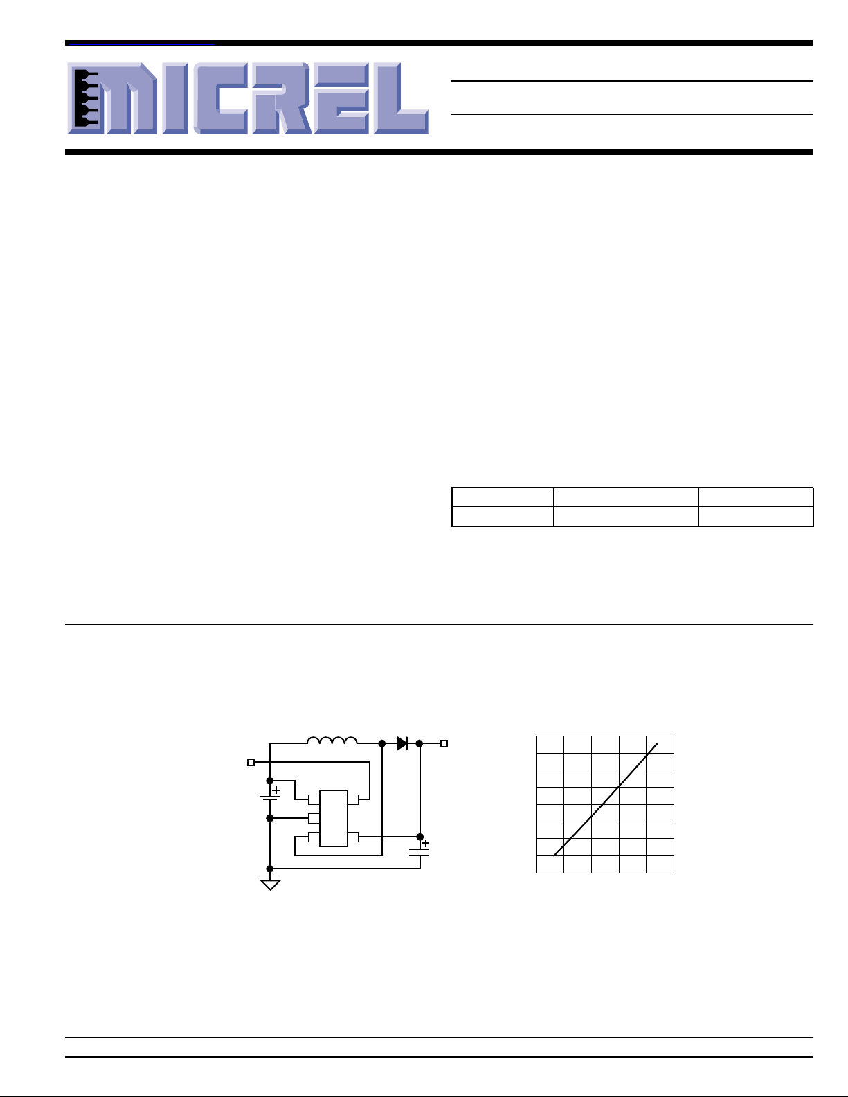
Typical Application
(from DAC)
VC*
10µH
MIC2141
15
2
34
10µF
Variable
V
OUT
(V)
V
vs. Output Voltage
4.0
3.5
3.0
2.5
2.0
C
1.5
1.0
0.5
0
0 5 10 15 20 25
DAC-Controlled LCD Bias Voltage Supply
Control Voltage
V
(V)
OUT
Micrel, Inc. • 1849 Fortune Drive • San Jose, CA 95131 • USA • tel + 1 (408) 944-0800 • fax + 1 (408) 944-0970 • http://www.micrel.com
June 2000 1 MIC2141
MIC2141 Micrel
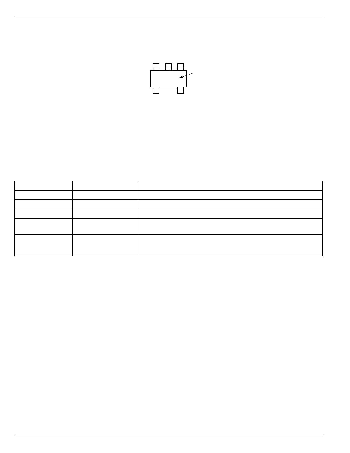
Pin Configuration
GND
2
IN
13
Part
Identification
VCFB
SW
SAxx
45
SOT-23-5 (BM)
Pin Description
Pin Number Pin Name Pin Function
1 IN Input: +2.5V to +14V supply for internal circuity.
2 GND Ground: Return for internal circuitry and internal MOSFET (switch) source.
3 SW Switch Node (Input): Internal MOSFET drain; 22V maximum.
4 FB Feedback (Input): Output voltage sense node. Compared to V
input voltage.
5 VC Control (Input): Output voltage control signal input. Input voltage of 0.8V to
3.6V is proportional to 4.8V to 22V output voltage (gain of 6). If the pin is not
connected, the output voltage will be VIN – 0.5V.
control
C
MIC2141 2 June 2000

MIC2141 Micrel
Absolute Maximum Ratings (Note 1)
Supply Voltage (VIN) ...................................................+18V
Switch Voltage (V
Feedback Voltage (F
Control Input Voltage (VC), Note 3 ..VIN–200mV ≤ VC ≤ 4V
ESD Rating, Note 4 ...................................................... 2kV
)..................................................+24V
SW
)................................................+24V
B
Operating Ratings (Note 2)
Supply Voltage (VIN) .................................... +2.5V to +14V
Switch Voltage (V
Ambient Temperature (T
Junction Tempgserature (TJ) ................... –40°C to +125°C
Package Thermal Resistance
)...................................... +3V to +22V
SW
).........................–40°C to +85°C
A
SOT-23-5 (θJA)......................................................220°C/W
Electrical Characteristics
VIN = 3.6V, V
Parameter Condition Min Typ Max Units
Input Voltage 2.5 14 V
Quiescent Current Switch off, VIN = 3.6V 70 100 µA
Comparator Hysteresis 10 mV
Control Voltage Gain (V
Controlled Output Voltage, VC = 0.8V; 2.5V ≤ VIN ≤ 4.2V 4.85 5.0 5.15 V
Note 3
Load Regulation 100µA ≤ I
Line Regulation 2.5V ≤ VIN ≤ 12V; I
Switch On-Resistance ISW = 100mA, VIN = 3.6V 4 Ω
Oscillator Frequency 300 330 360 kHz
Oscillator Duty Cycle 15 18 %
OUT
= 5V; I
= 1mA; TJ = 25°C, bold values indicate –40°C ≤ TA ≤ +85°C; unless noted.
OUT
) 2.5V ≤ VIN ≤ 12V, V
OUT/VC
VC = 2.5V; 2.7V ≤ VIN ≤ 12V 14.55 15.0 15.45 V
VC = 3.4V; 3.6V ≤ VIN ≤ 12V 19.4 20.0 20.6 V
ISW = 100mA, VIN = 12V 2.5 Ω
≤ 1mA, V
OUT
= 15V 6
OUT
= 15V 0.25 1 %
OUT
≤ 1mA 0.05 0.2 %/V
OUT
Note 1. Exceeding the absolute maximum rating may damage the device.
Note 2. The device is not guaranteed to function outside its operating rating.
Note 3. VC = 4V sets V
Note 4. Devices are ESD sensitive. Handling precautions recommended. Human body model, 1.5k in series with 100pF.
to 24V (absolute maximum level on VSW); VC must be ≤ VIN – 200mV.
OUT
June 2000 3 MIC2141
MIC2141 Micrel
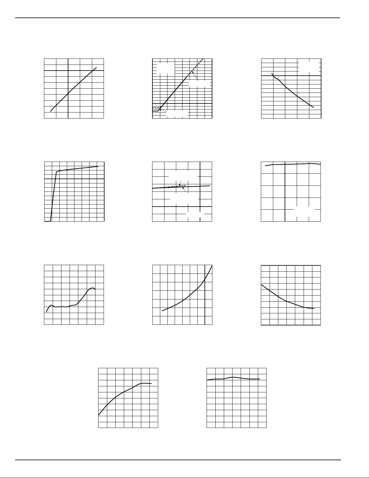
µ
Typical Characteristcs
Feedback Current
vs. Output Voltage
25
20
15
10
5
FEEDBACK CURRENT (µA)
0
0 5 10 15 20 25
OUTPUT VOLTAGE (V)
Control Current
vs. Control Voltage
7
6
5
4
3
2
1
CONTROL CURRENT (nA)
0
01234
CONTROL VOLTAGE (V)
Control Voltage
vs. Output Voltage
20
VIN = 5V
L = 33µH
15
= 100mA
L = 33
= 150mA
L = 22µH
VIN = 2.5V
H
VIN = 5V
10
5
OUTPUT VOLTAGE (V)
15.00
14.95
14.90
14.85
OUTPUT VOLTAGE (V)
14.80
VIN = 3.6V
0
01234
CONTROL VOLTAGE (V)
Load Regulation
I
PEAK
I
PEAK
012345
LOAD CURRENT (mA)
Gain
vs. Output Voltage
6.4
6.3
6.2
6.1
GAIN
6.0
5.9
5.8
5.7
0 5 10 15 20 25
OUTPUT VOLTAGE (V)
15.0
14.8
14.6
14.4
14.2
OUTPUT VOLTAGE (V)
14.0
Line Regulation
24681012
INPUT VOLTAGE (V)
VIN = 5V
L = 33µH
L = 33µH
I
= 100µA
L
Oscillator Frequency
400
380
360
340
FREQUENCY (kHz)
320
300
vs. Input Voltage
2 4 6 8 10121416
INPUT VOLTAGE (V)
Frequency
350
340
330
320
FREQUENCY (kHz)
310
300
vs. Temperature
-40 -20 0 20 40 60 80 100
TEMPERATURE (°C)
Quiescent Current
280
240
200
160
120
QUIESCENT CURRENT (µA)
vs. Input Voltage
80
40
0
0246810121416
INPUT VOLTAGE (V)
0.60
0.58
0.56
0.54
ON-TIME (µs)
0.52
0.50
Duty Cycle
vs. Temperature
20
19
18
17
16
15
14
13
DUTY CYCLE (%)
12
11
10
-40 -20 0 20 40 60 80 100
TEMPERATURE (°C)
On-Time
vs. Temperature
-40 -20 0 20 40 60 80 100
TEMPERATURE (°C)
MIC2141 4 June 2000

MIC2141 Micrel
14.00
14.20
14.40
14.60
14.80
15.00
-40 -20 0 20 40 60 80 100
OUTPUT VOLTAGE (V)
TEMPERATURE (°C)
0
10
20
30
40
50
60
70
80
90
100
01234
EFFICIENCY (%)
OUTPUT CURRENT (mA)
0
1
2
3
4
5
6
7
8
-40 -20 0 20 40 60 80 100
R
DS(on)
(Ω)
TEMPERATURE (°C)
Quiescent Current
vs. Temperature
88
86
84
82
80
QUIESCENT CURRENT (µA)
78
-40 -20 0 20 40 60 80 100
TEMPERATURE (°C)
VIN = 5V
Switch Voltage Drop
vs. Temperature
VIN = 3.3V
I
= 100mA
D
0
-40 -20 0 20 40 60 80 100
TEMPERATURE (°C)
(mV)
DS
V
800
700
600
500
400
300
200
100
Output Voltage
vs. Temperature
VIN = 5V
L = 33µH
Switch On-Resistance
vs. Temperature
VIN = 3.3V
Gain
6.00
5.98
5.96
GAIN
5.94
5.92
5.90
vs. Temperature
VIN = 5V
-40 -20 0 20 40 60 80 100
TEMPERATURE (°C)
Switch Voltage Drop
vs. Input Voltage
IDS = 100mA
0
2 4 6 8 10 12 14
INPUT VOLTAGE (V)
(mV)
DS
V
900
800
700
600
500
400
300
200
100
9
8
7
6
5
4
3
2
ON-RESISTANCE (Ω)
1
0
2 4 6 8 10 12 14
June 2000 5 MIC2141
On-Resistance vs.
Input Voltage
INPUT VOLTAGE (V)
Efficiency
BAT54HT1 Diode
1N4148 Diode
VIN = 5V
V
= 15V
OUT
L = 33µH
Ripple Voltage vs.
90
80
70
60
50
40
30
20
RIPPLE VOLTAGE (mV)
10
0
Input Voltage
L = 100µH
V
= 15V
OUT
I
= 1mA
L
24681012
INPUT VOLTAGE (V)
 Loading...