

MIC2085/2086 Micrel
查询MIC2085供应商
MIC2085/MIC2086
Single Channel Hot Swap Controllers
General Description
The MIC2085 and MIC2086 are single channel positive
voltage hot swap controllers designed to allow the safe
insertion of boards into live system backplanes. The MIC2085
and MIC2086 are available in 16-pin and 20-pin QSOP
packages, respectively. Using a few external components
and by controlling the gate drive of an external N-Channel
MOSFET device, the MIC2085/86 provide inrush current
limiting and output voltage slew rate control in harsh, critical
power supply environments. Additionally, a circuit breaker
function will latch the output MOSFET off if the current limit
threshold is exceeded for a programmed period of time. The
devices’ array of features provide a simplified yet robust
solution for many network applications in meeting the power
supply regulation requirements and affords protection of
critical downstream devices and components.
All support documentation can be found on Micrel’s web
site at www.micrel.com.
Features
• MIC2085: Pin for pin functional equivalent to the
LTC1642
• 2.3V to 16.5V supply voltage operation
• Surge voltage protection to 33V
• Operating temperature range –40°C to 85°C
• Active current regulation limits inrush current
independent of load capacitance
• Programmable inrush current limiting
• Analog foldback current limiting
• Electronic circuit breaker
• Dual-level overcurrent fault sensing
• Fast response to short circuit conditions (< 1µs)
• Programmable output undervoltage detection
• Undervoltage lockout protection
• Power-on reset (MIC2085/86) and
power-good (MIC2086) status outputs
• /FAULT status output
• Driver for SCR crowbar on overvoltage
Applications
• RAID systems
• Cellular base stations
• LAN servers
• WAN servers
• InfiniBand™ Systems
• Industrial high side switching
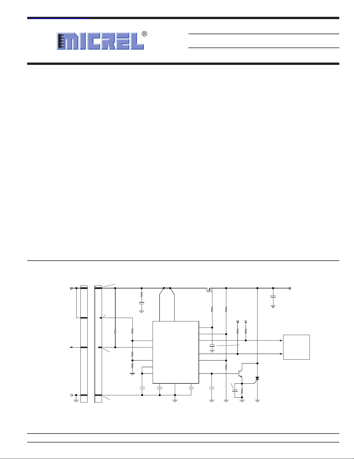
T ypical Application
(PowerPAK
/POR
FB
283
Q1
Si7884DP
14
11
10
5
7
1
C6
0.01µF
TM
SO-8)
*R6
10Ω
R7
127kΩ
1%
R10
47kΩ
R8
16.2kΩ
1%
C7
0.033µF
µ
s
V
LOGIC
C2
0.022µF
R11
47kΩ
Q2
2N4401
**R9
180Ω
C
LOAD
220µF
Output Signal
(Power Good)
Power-On Reset
Output
Q3
TCR22-4
V
OUT
12V@5A
PWRGD
LOGIC
CONTROLLER
/RESET
34
C1
µ
F
1
16 15
4
ON
6
/FAULT
9
OV
12
COMP—
13
REF
CPOR
C4
µ
F
0.1
R
SENSE
0.007Ω
2%
12
SENSEVCC
MIC2085
GATE
COMP+
COMPOUT
CRWBR
GND
CFILTER
C5
8200pF
POR/START-UP DELAY = 60ms
Circuit-Breaker Response Time = 500
*R6 is an optional component used for noise filtering
**R9 needed when using a sensitive gate SCR
V
12V
/FAULT
GND
IN
Backplane
Connector
PCB Edge
Connector
(or Short)
Long
Pin
Short
Pin
R5
47kΩ
Medium
Pin
Long
Pin
R2
100kΩ
1%
R3
1.82kΩ
1%
R4
10kΩ
1%
Overvoltage (Input) = 13.3V
Undervoltage Lockout = 10.8V
Undervoltage (Output) &
Power-Good (Output) = 11.4V
R1
3.3Ω
C3
µ
F
0.1
InfiniBand is a trademark of InfiniBand Trade Association
PowerPAK is a trademark of Vishay Intertechnology Inc.
Micrel, Inc. • 1849 Fortune Drive • San Jose, CA 95131 • USA • tel + 1 (408) 944-0800 • fax + 1 (408) 944-0970 • http://www.micrel.com
January 2004 1 M0235-121903
MIC2085/2086 Micrel
Ordering Information
Part Number Fast Circuit Breaker Threshold Discharge Output Package
MIC2085-xBQS x = J, 95mV NA 16-pin QSOP
x = K, 150mV*
x = L, 200mV*
x = M, Off
MIC2086-xBQS x = J, 95mV Yes 20-pin QSOP
x = K, 150mV*
x = L, 200mV*
x = M, Off
*Contact factory for availability.
Pin Configuration
CFILTER
CPOR
ON
/POR
/FAULT
FB
GND
1CRWBR
1CRWBR
2
3
4
5
6
7
8
16 VCC
SENSE
15
GATE
14
REF
13
COMP–
12
COMP+
11
COMPOUT
10
OV
9
CFILTER
PWRGD
CPOR
ON
/POR
/FAULT
FB
GND
GND
2
3
4
5
6
7
8
9
10
20 VCC
VCC
19
SENSE
18
GATE
17
REF
16
DIS
15
COMP–
14
COMP+
13
COMPOUT
12
OV
11
MIC2085
16-Pin QSOP (QS)
MIC2086
20-Pin QSOP (QS)
Pin Description
Pin Number Pin Number Pin Name Pin Function
MIC2086 MIC2085
1 1 CRWBR Overvoltage Timer and Crowbar Circuit Trigger: A capacitor connected to
this pin sets the timer duration for which an overvoltage condition will trigger
an external crowbar circuit. This timer begins when the OV input rises above
its threshold as an internal 45µA current source charges the capacitor. Once
the voltage reaches 470mV, the current increases to 1.5mA.
2 2 CFILTER Current Limit Response Timer: A capacitor connected to this pin defines the
period of time (t
fault condition and trip the circuit breaker. If no capacitor is connected, then
t
OCSLOW
OCSLOW
defaults to 5µs.
3 3 CPOR Power-On Reset Timer: A capacitor connected between this pin and ground
sets the start-up delay (t
VCC rises above the UVLO threshold, the capacitor connected to CPOR
begins to charge. When the voltage at CPOR crosses 1.24V, the start-up
threshold (V
C
POR
above V
CPOR rises above the power-on reset delay threshold (VTH), the timer
START
is immediately discharged to ground. When the voltage at FB rises
, capacitor C
FB
resets by pulling CPOR to ground, and /POR is deasserted.
If C
= 0, then t
POR
) in which an overcurrent event must last to signal a
) and the power-on reset interval (t
START
), a start cycle is initiated if ON is asserted while capacitor
begins to charge again. When the voltage at
POR
defaults to 20µs.
START
POR
). When
M0235-121903 2 January 2004

MIC2085/2086 Micrel
Pin Description (Cont.)
Pin Number Pin Number Pin Name Pin Function
MIC2086 MIC2085
4 4 ON ON Input: Active high. The ON pin, an input to a Schmitt-triggered compara-
tor used to enable/disable the controller, is compared to a VTH reference
with 100mV of hysteresis. Once a logic high is applied to the ON pin
> 1.24V), a start-up sequence is initiated as the GATE pin starts
(V
ON
ramping up towards its final operating voltage. When the ON pin receives a
low logic signal (V
high if VCC is above the UVLO threshold. ON must be low for at least 20µs
in order to initiate a start-up sequence. Additionally, toggling the ON pin
LOW to HIGH resets the circuit breaker.
5 5 /POR Power-On Reset Output: Open drain N-Channel device, active low. This pin
remains asserted during start-up until a time period t
voltage rises above the power-good threshold (V
C
determines t
POR
at the FB pin, /POR is asserted for a minimum of one timing cycle, t
/POR pin has a weak pull-up to VCC.
6 N/A PWRGD Power-Good Output: Open drain N-Channel device, active high. When the
voltage at the FB pin is lower than 1.24V, the PWRGD output is held low.
When the voltage at the FB pin is higher than 1.24V, then PWRGD is
asserted. A pull-up resistor connected to this pin and to VCC will pull the
output up to VCC. The PWRGD pin has a weak pull-up to VCC.
7 6 /FAULT Circuit Breaker Fault Status Output: Open drain N-Channel device, active
low. The /FAULT pin is asserted when the circuit breaker trips due to an
overcurrent condition. Also, this pin indicates undervoltage lockout and
overvoltage fault conditions. The /FAULT pin has a weak pull-up to VCC.
8 7 FB Power-Good Threshold Input: This input is internally compared to a 1.24V
reference with 3mV of hysteresis. An external resistive divider may be used
to set the voltage at this pin. If this input momentarily goes below 1.24V,
then /POR is activated for one timing cycle, t
undervoltage condition. The /POR signal de-asserts one timing cycle after
the FB pin exceeds the power-good threshold by 3mV. A 5µs filter on this pin
prevents glitches from inadvertently activating this signal.
9,10 8 GND Ground Connection: Tie to analog ground.
11 9 OV OV Input: When the voltage on OV exceeds its trip threshold, the GATE pin
is pulled low and the CRWBR timer starts. If OV remains above its threshold
long enough for CRWBR to reach its trip threshold, the circuit breaker is
tripped. Otherwise, the GATE pin begins to ramp up one POR timing cycle
after OV drops below its trip threshold.
12 10 COMPOUT Uncommitted Comparator’s Open Drain Output.
13 11 COMP+ Comparator’s Non-Inverting Input.
14 12 COMP- Comparator’s Inverting Input.
15 NA DIS Discharge Output: When the MIC2086 is turned off, a 550Ω internal resistor
at this output allows the discharging of any load capacitance to ground.
16 13 REF Reference Output: 1.24V nominal. Tie a 0.1µF capacitor to ground to ensure
stability.
17 14 GATE Gate Drive Output: Connects to the gate of an external N-Channel
MOSFET. An internal clamp ensures that no more than 13V is applied
between the GATE pin and the source of the external MOSFET. The GATE
pin is immediately brought low when either the circuit breaker trips or an
undervoltage lockout condition occurs.
< 1.14V), the GATE pin is grounded and /FAULT is
ON
after the FB pin
POR
). The timing capacitor
. When an output undervoltage condition is detected
POR
FB
, indicating an output
POR
POR
. The
January 2004 3 M0235-121903

MIC2085/2086 Micrel
Pin Description (Cont.)
Pin Number Pin Number Pin Name Pin Function
MIC2086 MIC2085
18 15 SENSE Circuit Breaker Sense Input: A resistor between this pin and VCC sets the
current limit threshold. Whenever the voltage across the sense resistor
exceeds the slow trip current limit threshold (V
is adjusted to ensure a constant load current. If V
exceeded for longer than time period t
OCSLOW
TRIPSLOW
, then the circuit breaker is
tripped and the GATE pin is immediately pulled low. If the voltage across the
sense resistor exceeds the fast trip circuit breaker threshold, V
any point due to fast, high amplitude power supply faults, then the GATE pin
is immediately brought low without delay. To disable the circuit breaker, the
SENSE and VCC pins can be tied together.
The default V
TRIPFAST
are available: 150mV, 200mV, or OFF(V
factory for availability of other options.
for either device is 95mV. Other fast trip thresholds
TRIPFAST
19,20 16 VCC Positive Supply Input: 2.3V to 16.5V. The GATE pin is held low by an
internal undervoltage lockout circuit until VCC exceeds a threshold of 2.18V.
If VCC exceeds 16.5V, an internal shunt regulator protects the chip from
VCC and SENSE pin voltages up to 33V.
), the GATE voltage
TRIPSLOW
(48mV) is
TRIPFAST
, at
disabled). Please contact
M0235-121903 4 January 2004

MIC2085/2086 Micrel
Absolute Maximum Ratings
(1)
(All voltages are referred to GND)
Supply Voltage (VCC) ..................................... –0.3V to 33V
SENSE Pin..........................................–0.3V to VCC + 0.3V
GATE Pin ....................................................... –0.3V to 22V
ON, DIS, /POR, PWRGD, /FAULT,
COMP+, COMP–, COMPOUT ....................... –0.3V to 20V
CRWBR, FB, OV, REF..................................... –0.3V to 6V
Maximum Currents
Digital Output Pins .....................................................10mA
(/POR, /FAULT, PWRGD, COMPOUT)
DIS Pin .......................................................................30mA
ESD Rating:
Human Body Model...................................................2kV
Machine Model........................................................200V
Operating Ratings
Supply Voltage (VCC) .................................... 2.3V to 16.5V
Operating Temperature Range .................. –40°C to +85°C
Junction Temperature (TJ) ........................................ 125°C
Package Thermal Resistance R
16-pin QSOP.....................................................112°C/W
20-pin QSOP.......................................................91°C/W
(2)
θ(J-A)
Electrical Characteristics
(3)
VCC = 5.0V, TA = 25°C unless otherwise noted. Bold indicates specifications over the full operating temperature range of –40°C to +85°C.
Symbol Parameter Condition Min Typ Max Units
V
CC
I
CC
V
UV
V
UVHYST
V
FB
V
FBHYST
V
OV
∆V
OV
V
OVHYST
I
OV
V
TH
I
CPOR
Supply Voltage 2.3 16.5 V
Supply Current 1.6 2.5 mA
Undervoltage Lockout Threshold VCC rising 2.05 2.18 2.28 V
VCC falling 1.85 2.0 2.10 V
UV Lockout Hysteresis 180 mV
FB (Power-Good) Threshold Voltage FB rising 1.19 1.24 1.29 V
FB Hysteresis 3mV
OV Pin Threshold Voltage OV pin rising 1.19 1.24 1.29 mV
OV Pin Threshold Voltage 2.3V < VCC < 16.5V 5 15 mV
Line Regulation
OV Pin Hysteresis 3mV
OV Pin Current 0.2 µA
POR Delay and Overcurrent (CFILTER) V
Timer Threshold
CPOR
, V
CFILTER
rising 1.19 1.24 1.29 V
Power-On Reset Timer Current Timer on –2.5 –2.0 –1.5 µA
Timer off 5 mA
I
TIMER
Current Limit /Overcurrent Timer on –30 –20 –15 µA
Timer Current (CFILTER) Timer off 2.5 mA
V
∆V
I
CR
V
CR
CR
TRIP
CRWBR Pin Threshold Voltage 2.3V < VCC < 16.5V 445 470 495 mV
CRWBR Pin Threshold Voltage 2.3V < VCC < 16.5V 4 15 mV
Line Regulation
CRWBR Pin Current CRWBR On, V
CRWBR On, V
CRWBR Off, V
Circuit Breaker Trip Voltage V
(Current Limit Threshold) 2.3V ≤ V
TRIP
= VCC –V
≤ 16.5V V
CC
= 0V –60 –45 –30 µA
CRWBR
= 2.1V –1.5 –1.0 mA
CRWBR
= 1.5V 3.3 mA
CRWBR
SENSE
V
TRIPSLOW
TRIPFAST
x = K 150 mV
x = J 80 95 110 mV
40 48 55 mV
x = L 200 mV
V
GS
External Gate Drive V
GATE
– V
CC
VCC < 3V 4 8 9 V
5V < VCC < 9V 11 12 13 V
9V < VCC < 15.0V 4.5 21–V
CC
13 V
January 2004 5 M0235-121903

MIC2085/2086 Micrel
Electrical Characteristics (Cont.)
Symbol Parameter Condition Min Typ Max Units
I
GATE
I
GATEOFF
V
ON
V
ONHYST
I
ON
V
START
V
OL
I
PULLUP
V
REF
∆V
LNR
∆V
LDR
I
RSC
V
COS
V
CHYST
R
DIS
GATE Pin Pull-up Current Start cycle, V
=16.5V –22 –16 –8 µA
V
CC
GATE
= 0V
VCC = 2.3V –20 –14 –8 µA
GATE Pin Sink Current /FAULT = 0, V
V
= 16.5V 25 50 mA
CC
GATE
>1V
VCC = 2.3V 12 20 mA
ON Pin Threshold Voltage ON rising 1.19 1.24 1.29 V
ON falling 1.09 1.14 1.19 V
ON Pin Hysteresis 100 mV
ON Pin Input Current VON = V
Undervoltage Start-up V
Timer Threshold
/FAULT, /POR, PWRGD Output I
Voltage (PWRGD for MIC2086 only)
OUT
CC
rising 1.19 1.24 1.29 V
CPOR
= 1.6mA 0.4 V
0.5 µA
Output Signal Pull-up Current /FAULT, /POR, PWRGD = GND –20 µA
/FAULT, /POR, PWRGD, COMPOUT (PWRGD for MIC2086 only)
Reference Output Voltage I
LOAD
= 0mA; C
= 0.1µF 1.21 1.24 1.27 V
REF
Reference Line Regulation 2.3V < VCC < 16.5V 5 10 mV
Reference Load Regulation I
Reference Short-Circuit Current V
Comparator Offset Voltage VCM = V
Comparator Hysteresis VCM = V
= 1mA 2.5 7.5 mV
OUT
= 0V 3.5 mA
REF
REF
REF
–5 5 mV
3mV
Discharge Pin Resistance ON pin toggles from HI to LOW 100 550 1000 Ω
AC Electrical Characteristics
(4)
Symbol Parameter Condition Min Typ Max Units
t
OCFAST
t
OCSLOW
t
ONDLY
t
FBDLY
Notes:
1. Exceeding the absolute maximum rating may damage the device.
2. The device is not guaranteed to function outside its operating rating.
3. Specification for packaged product only.
4. Specification for packaged product only.
Fast Overcurrent Sense to GATE VCC = 5V 1 µs
Low Trip Time V
C
–V
CC
GATE
= 100mV
SENSE
= 10nF, See Figure 1
Slow Overcurrent Sense to Gate VCC = 5V 5 µs
Low Trip Time V
CC
C
FILTER
–V
= 50mV
SENSE
= 0, See Figure 1
ON Delay Filter 20 µs
FB Delay Filter 20 µs
M0235-121903 6 January 2004
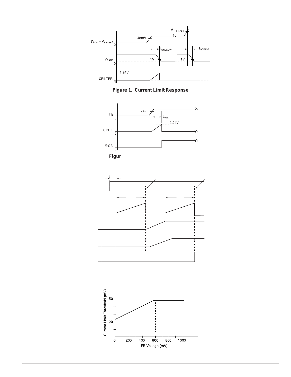
MIC2085/2086 Micrel
1V
48mV
V
GATE
t
OCSLOW
V
TRIPFAST
(VCCÐV
SENSE
)
t
OCFAST
1V
0
CFILTER
0
0
1.24V
Timing Diagrams
Figure 1. Current Limit Response
ON
CPOR
GATE
FB
FB
CPOR
/POR
0
0
0
1.24V
t
POR
Figure 2. Power-On Reset Response
t
ONDLY
1.24V
0
1.24V
0
0
0
Arm Fast Comparator
t
START
1.24V
Arm Slow Comparator
t
POR
1.24V
/POR
0
Figure 3. Power-On Start-Up Delay Timing
50
January 2004 7 M0235-121903
20
Current Limit Threshold (mV)
0
600 800 1000
400200
FB Voltage (mV)
Figure 4. Foldback Current Limit Response
MIC2085/2086 Micrel
g
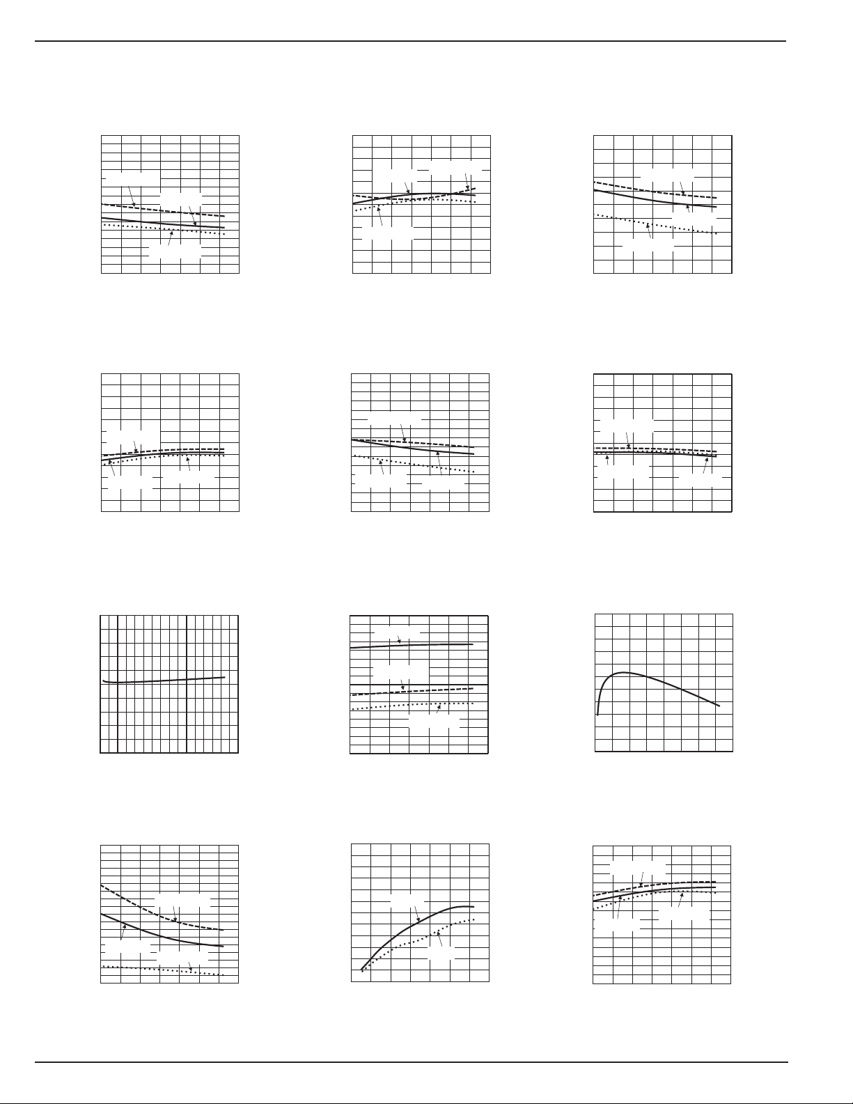
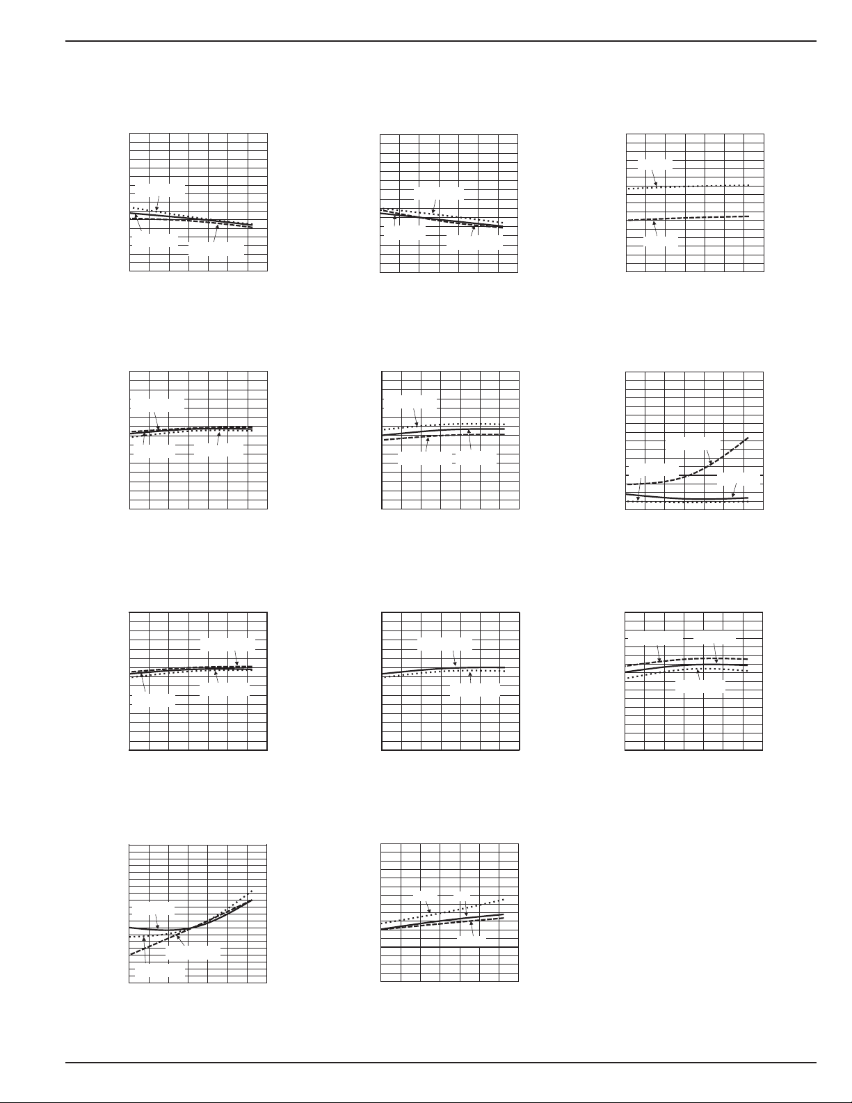
Typical Characteristics
Supply Current
4.0
vs. Temperature
3.5
3.0
V
= 16.5V
CC
2.5
2.0
VCC= 5V
1.5
1.0
SUPPLY CURRENT (mA)
0.5
0.0
-40 -20 0 20 40 60 80 100
Overcurrent Timer Current
34
VCC= 2.3V
TEMPERATURE (°C)
vs. Temperature
30
26
(µA)
VCC= 16.5V
22
TIMER
I
18
VCC= 5V
14
10
-40 -20 0 20 40 60 80 100
VCC= 2.3V
TEMPERATURE (°C)
Power-On Reset Timer Current
vs. Temperature
2.6
(µA)
CPOR
I
2.4
2.2
2.0
1.8
VCC= 5V
VCC= 2.3V
VCC= 16.5V
1.6
1.4
-40 -20 0 20 40 60 80 100
TEMPERATURE (°C)
Overcurrent Timer (Off) Current
vs. Temperature
5
4
VCC= 16.5V
3
(mA)
2
TIMER
I
VCC= 2.3V
1
0
-40 -20 0 20 40 60 80 100
TEMPERATURE (°C)
VCC= 5V
Power-On Reset Timer (Off) Current
10
vs. Temperature
9
(mA)
I
CPOR
8
7
6
5
4
3
2
VCC= 16.5V
VCC= 5V
VCC= 2.3V
1
0
-40 -20 0 20 40 60 80 100
TEMPERATURE (°C)
Gate Pull-Up Current
vs. Temperature
30
25
20
VCC= 16.5V
(µA)
15
GATE
I
10
VCC= 2.3V
5
0
-40 -20 0 20 40 60 80 100
TEMPERATURE (°C)
VCC= 5V
Gate Pull-Up Current
vs. V
25
20
15
(A)
10
GATE
I
5
0
2 4 6 8 10 12 14 16 18
Gate Sink Current
100
vs. Temperature
CC
(V)
V
CC
90
80
(mA)
70
60
VCC= 16.5V
50
GATEOFF
40
I
VCC= 5V
30
VCC= 2.3V
20
10
-40 -20 0 20 40 60 80 100
TEMPERATURE (°C)
External Gate Drive
vs. Temperature
16
VCC= 5V
14
12
10
8
6
4
VCC= 16.5V
VCC= 2.3V
(V)
GS
V
2
0
-40 -20 0 20 40 60 80 100
TEMPERATURE (°C)
Gate Sink Current
600
vs. Gate Volta
500
400
(mA)
300
GATEOFF
200
I
100
0
02468101214
12V
V
CC
GATE
5V
CC
(V)
External Gate Drive
vs. V
22
20
18
16
14
(V)
12
GS
10
V
8
6
4
2
0
2 4 6 8 10 12 14 16 18
POR Delay/Overcurrent
e
(mV)
V
TH
1.25
1.24
1.23
1.22
1.21
1.20
Timer Threshold
vs. Temperature
VCC= 16.5V
VCC= 5V
-40 -20 0 20 40 60 80 100
TEMPERATURE (°C)
CC
(V)
V
CC
VCC= 2.3V
M0235-121903 8 January 2004
MIC2085/2086 Micrel
1.7
1.8
1.9
2.0
2.1
2.2
2.3
2.4
2.5
-40 -20 0 20 40 60 80 100
UVLO THRESHOLD (V)
TEMPERATURE (°C)
10
14
18
22
26
-40 -20 0 20 40 60 80 100
I
PULLUP
(µA)
TEMPERATURE (°C)
Output Signal Pull-Up Current
vs. Temperature
VCC= 16.5V
VCC= 2.3V
VCC= 5V
Typical Characteristics
Current Limit Threshold
(Fast Trip)
120
115
110
105
(mV)
100
TRIPFAST
V
1.30
1.25
1.20
ON THRESHOLD (V)
1.15
vs. Temperature
VCC= 2.3V
95
90
VCC= 5V
85
80
-40 -20 0 20 40 60 80 100
ON Pin Threshold (Rising)
VCC= 16.5V
VCC= 5V
-40 -20 0 20 40 60 80 100
VCC= 16.5V
TEMPERATURE (°C)
vs. Temperature
VCC= 2.3V
TEMPERATURE (°C)
Current Limit Threshold
(Slow Trip)
vs. Temperature
55
53
(mV)
51
49
TRIPSLOW
V
47
45
-40 -20 0 20 40 60 80 100
1.20
1.15
1.10
ON THRESHOLD (V)
1.05
VCC= 2.3V
VCC= 5V
TEMPERATURE (°C)
ON Pin Threshold (Falling)
vs. Temperature
VCC= 2.3V
VCC= 16.5V
-40 -20 0 20 40 60 80 100
VCC= 16.5V
VCC= 5V
TEMPERATURE (°C)
UVLO Threshold
vs. Temperature
UVLO+
UVLO–
ON Pin Input Current
vs. Temperature
40
35
30
25
20
15
10
5
ON PIN INPUT CURRENT (nA)
0
-40 -20 0 20 40 60 80 100
VCC= 16.5V
VCC= 2.3V
TEMPERATURE (°C)
VCC= 5V
FB (Power-Good) Threshold
1.30
1.25
1.20
FB THRESHOLD (V)
1.15
-40 -20 0 20 40 60 80 100
Comparator Offset Voltage
0.5
0.4
0.3
January 2004 9 M0235-121903
0.2
0.1
0.0
-40 -20 0 20 40 60 80 100
COMPARATOR OFFSET VOLTAGE (V)
vs. Temperature
VCC= 5V
TEMPERATURE (°C)
vs. Temperature
VCC= 5V
VCC= 16.5V
VCC= 2.3V
TEMPERATURE (°C)
VCC= 16.5V
VCC= 2.3V
Overvoltage Pin Threshold
1.30
1.25
1.20
1.15
OVERVOLTAGE PIN THRESHOLD (V)
1000
900
800
700
(Ω)
600
DIS
500
R
400
300
200
vs. Temperature
VCC= 16.5V
VCC= 2.3V
-40 -20 0 20 40 60 80 100
TEMPERATURE (°C)
Discharge Pin Resistance
vs. Temperature
2.3V
5V
16.5V
-40 -20 0 20 40 60 80 100
TEMPERATURE (°C)

MIC2085/2086 Micrel
Test Circuit
V
12V
R
I
IN
IN
C1
0.47mF
R2
154k
W
1%
R3
20k
1%
4
ON
W
SW1
ON/OFF
SENSE
0.01
W
5%
12
34
19,20 18
VCC
SENSE
MIC2086
Si7892DP
(PowerPAK
17
GATE
8
FB
5
/POR
Q1
TM
SO-8)
R1
10
W
C2
0.022mF
Downstream
Signal
R4
97.6k
1%
R5
12.4k
1%
I
OUT
V
OUT
R
LOAD
C
LOAD
W
W
Not all pins shown for clarity.
C3
0.047mF
GNDCPOR CFILTER
9,10 23
DIS
C4
0.047mF
15
SW2
DIS
R6
4.4k
W
C5
0.033mF
R7
1.5k
W
Q2
ZTX788A
R8
330
W
Q3
TCR22-4
M0235-121903 10 January 2004

MIC2085/2086 Micrel
Functional Characteristics
CC
V
ON
C
OUT
I
IN =
I
CC
V
/FAULT
V
POR
OUT
5V/div
1V/div
1V/div
1A/div
5V/div
10V/div
10V/div
12V Hot Insert Response
C
TIME (20ms/div.)
Inrush Current Response
C
R
LOAD =
LOAD =
R
LOAD =
LOAD =
V
IN =
1000µF
V
IN =
5700µF
12V
4.8Ω
12V
3.4Ω
ON
POR
C
OUT
V
/POR
ON
OUT
V
FB
1V/div
1V/div
5V/div
10V/div
1V/div
5V/div
1V/div
12V Turn On Response
TIME (20ms/div.)
Power-Good Response
C
LOAD =
C
R
LOAD =
R
LOAD =
LOAD =
V
IN =
1000µF
V
IN =
1000µF
12V
4.8Ω
12V
4.8Ω
IN
I
ON
GATE
= I
I
V
OUT
IN
OUT
1A/div
1V/div
20V/div
2A/div
5V/div
TIME (10ms/div.)
Turn Off — Normal Discharge
V
(External) = 0
R
DIS
R
LOAD =
C
LOAD =
SW2 = HIGH
TIME (2.5ms/div.)
12V
IN =
4.8Ω
1000µF
PG
ON
GATE
= I
I
V
OUT
IN
OUT
10V/div
1V/div
20V/div
2A/div
5V/div
TIME (10ms/div.)
Turn Off — Crowbar Discharge
V
R
LOAD =
C
LOAD =
SW2 = LOW
TIME (2.5ms/div.)
12V
IN =
4.8Ω
1000µF
January 2004 11 M0235-121903

MIC2085/2086 Micrel
Functional Characteristics (continued)
Turn On Into Short Circuit
ON
1V/div
1V/div
CFILTER
/FAULT
V
OUT
10V/div
5V/div
C
LOAD =
V
IN =
R
LOAD =
1000µF
12V
0
TIME (10ms/div.)
M0235-121903 12 January 2004

MIC2085/2086 Micrel
Functional Block Diagram
MIC2086
SENSE
VCC
CFILTER
GND
FB
CPOR
18 (15)
19,20 (16)
2 (2)
9,10 (8)
8 (7)
3 (3)
20mA
20mA
20mA
17 (14)
16 (13)
12 (10)
13 (11)
14 (12)
7 (6)
5 (5)
15
6
GATE
REF
COMPOUT
COMP+
COMPÐ
DIS*
/FAULT
/POR
PWRGD*
Charge
Pump
48mV
+
Ð
13V
1.24V
+
Ð
95mV
V
REG1
V
CC1
20mA
CC1
UVLO
2.2V
Circuit Breaker
Response
or
UVLO
REG2
+
Ð
21V
550
W
V
CC1
V
CC1
+
1.24V
1.24V
Ð
+
Glitch
Ð
Filter
Logic
V
CC1
1.5mA
V
CC1
V
CC1
45mA
V
CC1
2.5mA
1.24V
+
Ð
+
Ð
0.45V
1 (1)
CRWBR
ON
4 (4)
1.24V
*DIS and PWRGD are not available on MIC2085.
Pin numbers for MIC2085 are in parenthesis ( ) where applicable.
+
Glitch
Ð
Filter
Glitch
Filter
+
Ð
1.24V
11 (9)
OV
MIC2086 Block Diagram
January 2004 13 M0235-121903

MIC2085/2086 Micrel
Functional Description
Hot Swap Insertion
When circuit boards are inserted into live system backplanes
and supply voltages, high inrush currents can result due to
the charging of bulk capacitance that resides across the
supply pins of the circuit board. This inrush current, although
transient in nature, may be high enough to cause permanent
damage to on-board components or may cause the system’s
supply voltages to go out of regulation during the transient
period which may result in system failures. The MIC2085/86
acts as a controller for external N-Channel MOSFET devices
in which the gate drive is controlled to provide inrush current
limiting and output voltage slew rate control during hot plug
insertions.
Power Supply
VCC is the supply input to the MIC2085/86 controller with a
voltage range of 2.3V to 16.5V. The VCC input can withstand
transient spikes up to 33V. In order to help suppress transients and ensure stability of the supply voltage, a capacitor
of 1.0µF to 10µF from VCC to ground is recommended.
Alternatively, a low pass filter, shown in the typical application
circuit, can be used to eliminate high frequency oscillations as
well as help suppress transient spikes.
Start-Up Cycle
When the voltage on the ON pin rises above its threshold of
1.24V, the MIC2085/86 first checks that its supply (VCC) is
above the UVLO threshold. If so, the device is enabled and
an internal 2µA current source begins charging capacitor
C
to 1.24V to initiate a start-up sequence (i.e., start-up
POR
delay times out). Once the start-up delay (t
CPOR is pulled immediately to ground and a 15µA current
source begins charging the GATE output to drive the external
MOSFET that switches VIN to V
. The programmed start-
OUT
up delay is calculated using the following equation:
V
tC
START POR
=× ≅× µ
TH
I
CPOR
0.62 C ( F)
POR
where VTH, the POR delay threshold, is 1.24V, and I
the POR timer current, is 2µA. As the GATE voltage continues ramping toward its final value (VCC + VGS) at a defined
slew rate (See
nated Start-Up”
“Load Capacitance”/“Gate Capacitance Domi-
sections), a second CPOR timing cycle
begins if: 1)/FAULT is high and 2)CFILTER is low (i.e., not
an overvoltage, undervoltage lockout, or overcurrent state).
This second timing cycle, t
, starts when the voltage at the
POR
FB pin exceeds its threshold (VFB) indicating that the output
voltage is valid. The time period t
is equivalent to t
POR
and sets the interval for the /POR to go Low-to-High after
“power is good” (See Figure 2 of
“Timing Diagrams”
current regulation is employed to limit the inrush current
transient response during start-up by regulating the load
current at the programmed current limit value (See
Limiting and Dual-Level Circuit Breaker”
section). The following equation is used to determine the nominal current
limit value:
V
I
LIM
TRIPSLOW
==
R
SENSE SENSE
48mV
R
START
) elapses,
(1)
CPOR
START
). Active
“Current
(2)
where V
TRIPSLOW
in the electrical table and R
is the current limit slow trip threshold found
is the selected value that
SENSE
will set the desired current limit. There are two basic start-up
modes for the MIC2085/86: 1)Start-up dominated by load
capacitance and 2)start-up dominated by total gate capacitance. The magnitude of the inrush current delivered to the
load will determine the dominant mode. If the inrush current
is greater than the programmed current limit (I
LIM
capacitance is dominant. Otherwise, gate capacitance is
dominant. The expected inrush current may be calculated
using the following equation:
C
LOAD
C
GATE
GATE
15 A
is the total GATE capacitance
where I
INRUSH I
GATE
≅× ≅µ×
GATE
is the GATE pin pull-up current, C
load capacitance, and C
(C
of the external MOSFET and any external capacitor
ISS
C
C
LOAD
GATE
connected from the MIC2085/86 GATE pin to ground).
Load Capacitance Dominated Start-Up
In this case, the load capacitance, C
, is large enough to
LOAD
cause the inrush current to exceed the programmed current
limit but is less than the fast-trip threshold (or the fast-trip
threshold is disabled, ‘M’ option). During start-up under this
condition, the load current is regulated at the programmed
current limit value (I
) and held constant until the output
LIM
voltage rises to its final value. The output slew rate and
equivalent GATE voltage slew rate is computed by the
following equation:
I
Output Voltage Slew Rate, dV /dt
where I
quently, the value of C
is the programmed current limit value. Conse-
LIM
must be selected to ensure that
FILTER
the overcurrent response time, t
OUT
OCSLOW
LIM
=
C
LOAD
, exceeds the time
needed for the output to reach its final value. For example,
given a MOSFET with an input capacitance C
4700pF, C
is 2200µF, and I
LOAD
is set to 6A with a 12V
LIMIT
ISS
input, then the load capacitance dominates as determined by
the calculated INRUSH > I
,
. Therefore, the output voltage
LIM
slew rate determined from Equation 4 is:
Output Voltage Slew Rate, dV /dt
and the resulting t
OCSLOW
approximately 4.5ms. (See
Overcurrent Timer Delays”
GATE Capacitance Dominated Start-Up
OUT
needed to achieve a 12V output is
“Power-On Reset, Start-Up, and
section to calculate t
=
2200 F
6A
µ
In this case, the value of the load capacitance relative to the
GATE capacitance is small enough such that the load current
during start-up never exceeds the current limit threshold as
determined by Equation 3. The minimum value of C
will ensure that the current limit is never exceeded is given by
the equation below:
I
C (min)
GATE
GATE
=×
I
LIM
C
LOAD
), then load
(3)
is the
LOAD
(4)
= C
GATE
V
2.73
=
ms
GATE
.)
that
OCSLOW
(5)
=
M0235-121903 14 January 2004

MIC2085/2086 Micrel
where C
capacitance (C
connected to the GATE pin of the MOSFET. Once C
is the summation of the MOSFET input
GATE
) and the value of the external capacitor
ISS
GATE
is
determined, use the following equation to determine
the output slew rate for gate capacitance dominated start-up.
I
dV /dt (output)
OUT
Table 1 depicts the output slew rate for various values of C
I
GATE
C
GATE
0.001µF 15V/ms
0.01µF 1.5V/ms
0.1µF 0.150V/ms
1µF 0.015V/ms
GATE
=
C
GATE
= 15µA
dV
OUT
(6)
GATE
/dt
Table 1. Output Slew Rate Selection for GATE
Capacitance Dominated Start-Up
Current Limiting and Dual-Level Circuit Breaker
Many applications will require that the inrush and steady state
supply current be limited at a specific value in order to protect
critical components within the system. Connecting a sense
resistor between the VCC and SENSE pins sets the nominal
current limit value of the MIC2085/86 and the current limit is
calculated using Equation 2. However, the MIC2085/86 exhibits foldback current limit response. The foldback feature
allows the nominal current limit threshold to vary from 24mV
up to 48mV as the FB pin voltage increases or decreases.
When FB is at 0V, the current limit threshold is 24mV and for
FB ≥ 0.6V, the current limit threshold is the nominal 48mV.
(See Figure 4 for Foldback Current Limit Response characteristic).
The MIC2085/86 also features a dual-level circuit breaker
triggered via 48mV and 95mV current limit thresholds sensed
across the VCC and SENSE pins. The first level of the circuit
breaker functions as follows. Once the voltage sensed across
these two pins exceeds 48mV, the overcurrent timer, its
duration set by capacitor C
, starts to ramp the voltage
FILTER
at CFILTER using a 2µA constant current source. If the
voltage at CFILTER reaches the overcurrent timer threshold
(VTH) of 1.24V, then CFILTER immediately returns to ground
as the circuit breaker trips and the GATE output is immediately shut down. For the second level, if the voltage sensed
across VCC and SENSE exceeds 95mV at any time, the
circuit breaker trips and the GATE shuts down immediately,
bypassing the overcurrent timer period. To disable current
limit and circuit breaker operation, tie the SENSE and VCC
pins together and the CFILTER pin to ground.
Output Undervoltage Detection
The MIC2085/86 employ output undervoltage detection by
monitoring the output voltage through a resistive divider
connected at the FB pin. During turn on, while the voltage at
the FB pin is below the threshold (VFB), the /POR pin is
asserted low. Once the FB pin voltage crosses VFB, a 2µA
current source charges capacitor C
voltage reaches 1.24V, the time period t
CPOR pin is pulled to ground and the /POR pin goes HIGH.
.
If the voltage at FB drops below VFB for more than 10µs, the
. Once the CPOR pin
POR
elapses as the
POR
/POR pin resets for at least one timing cycle defined by t
(see Applications Information for an example).
Input Overvoltage Protection
The MIC2085/86 monitors and detects overvoltage conditions in the event of excessive supply transients at the input.
Whenever the overvoltage threshold (VOV) is exceeded at
the OV pin, the GATE is pulled low and the output is shut off.
The GATE will begin ramping one POR timing cycle after the
OV pin voltage drops below its threshold. An external CRWBR
circuit, as shown in the typical application diagram, provides
a time period that an overvoltage condition must exceed in
order to trip the circuit breaker. When the OV pin exceeds the
overvoltage threshold (VOV), the CRWBR timer begins charging the CRWBR capacitor initially with a 45µA current source.
Once the voltage at CRWBR exceeds its threshold (VCR) of
0.47V, the CRWBR current immediately increases to 1.5mA
and the circuit breaker is tripped, necessitating a device reset
by toggling the ON pin LOW to HIGH.
Power-On Reset, Start-Up, and Overcurrent Timer
Delays
The Power-On Reset delay, t
, is the time period for the
POR
/POR pin to go HIGH once the voltage at the FB pin exceeds
the power-good threshold (VTH). A capacitor connected to
CPOR sets the interval, t
start-up delay, t
(see Equation 1).
START
POR
, and t
is equivalent to the
POR
A capacitor connected to CFILTER is used to set the timer
which activates the circuit breaker during overcurrent conditions. When the voltage across the sense resistor exceeds
the slow trip current limit threshold of 48mV, the overcurrent
timer begins to charge for a period, t
C
defaults to 5µs. If t
. If no capacitor is used at CFILTER, then t
FILTER
OCSLOW
elapses, then the circuit breaker
OCSLOW
, determined by
is activated and the GATE output is immediately pulled to
ground. The following equation is used to determine the
overcurrent timer period, t
tC
OCSLOW
=×≅×µ
FILTER
OCSLOW
V
I
TIMER
.
TH
0.062 C ( F)
FILTER
where VTH, the CFILTER timer threshold, is 1.24V and
I
, the overcurrent timer current, is 20µA. Tables 2 and
TIMER
3 provide a quick reference for several timer calculations
using select standard value capacitors.
POR
OCSLOW
(7)
January 2004 15 M0235-121903

MIC2085/2086 Micrel
C
POR
t
POR
= t
START
0.01µF 6ms
0.02µF 12ms
0.033µF 18.5ms
0.05µF 30ms
0.1µF 60ms
0.33µF 200ms
Table 2. Selected Power-On Reset and
Start-Up Delays
C
FILTER
t
OCSLOW
1800pF 100µs
4700pF 290µs
8200pF 500µs
0.010µF 620µs
0.020µF 1.2ms
0.033µF 2.0ms
0.050µF 3.0ms
0.1µF 6.2ms
0.33µF 20.75ms
Table 3. Selected Overcurrent Timer Delays
Applications Information
Output Undervoltage Detection
For output undervoltage detection, the first consideration is to
establish the output voltage level that indicates “power is
good.” For this example, the output value for which a 12V
supply will signal “good” is 11V. Next, consider the tolerances
of the input supply and FB threshold (VFB). For this example,
the 12V supply varies ±5%, thus the resulting output voltage
may be as low as 11.4V and as high as 12.6V. Additionally,
the FB threshold has ±50mV tolerance and may be as low as
1.19V and as high as 1.29V. Thus, to determine the values of
the resistive divider network (R5 and R6) at the FB pin, shown
in Figure 5, use the following iterative design procedure.
1) Choose R6 so as to limit the current through the
divider to approximately 100µA or less.
V
FB(MAX)
R6
≥
100 A
µ
R6 is chosen as 13.3kΩ ± 1%.
2) Next, determine R5 using the output “good”
voltage of 11V and the following equation:
VV
OUT(Good)
1.29V
≥
100 A
=
FB
≥Ω
µ
R5 R6
+
()
R6
12.9k
.
(8)
Using some basic algebra and simplifying Equation 8 to
isolate R5, yields:
–1
OUT(Good)
(8.1)
= 11V, and R6 is
R5 R6
where V
=
FB(MAX)
V
OUT(Good)
V
FB(MAX)
= 1.29V, V
13.3kΩ. Substituting these values into Equation 8.1 now
yields R5 = 100.11kΩ. A standard 100kΩ ± 1% is selected.
Now, consider the 11.4V minimum output voltage, the lower
tolerance for R6 and higher tolerance for R5, 13.17kΩ and
101kΩ, respectively. With only 11.4V available, the voltage
sensed at the FB pin exceeds V
FB(MAX)
, thus the /POR and
PWRGD (MIC2086) signals will transition from LOW to
HIGH, indicating “power is good” given the worse case
tolerances of this example.
Input Overvoltage Protection
The external CRWBR circuit shown in Figure 5 consists of
capacitor C4, resistor R7, NPN transistor Q2, and SCR Q3.
The capacitor establishes a time duration for an overvoltage
condition to last before the circuit breaker trips. The CRWBR
timer duration is approximated by the following equation:
t
OVCR
()
≅
I
CR
CR
≅×µ0
.01 C4( F)
(9)
C4 V
×
where VCR, the CRWBR pin threshold, is 0.47V and ICR, the
CRWBR pin current, is 45µA during the timer period (see the
CRWBR timer pin description for further description). A
similar design approach as the previous undervoltage detection example is recommended for the overvoltage protection
circuitry, resistors R2 and R3 in Figure 5. For input overvoltage protection, the first consideration is to establish the input
voltage level that indicates an overvoltage triggering a system (output voltage) shut down. For this example, the input
value for which a 12V supply will signal an “output shut down”
is 13.2V (+10%). Similarly, from the previous example:
1) Choose R3 to satisfy 100µA condition.
R3
≥
V
OV(MIN)
100 A
µ
1.19V
≥
100 A
≥Ω
11.9k
µ
.
R3 is chosen as 13.7kΩ ±1%.
2) Thus, following the previous example and
substituting R2 and R3 for R5 and R6, respectively, and 13.2V overvoltage for 11V output
“good”, the same formula yields R2 of 138.3kΩ.
The next highest standard 1% value is 140kΩ.
Now, consider the 12.6V maximum input voltage (V
CC
+5%),
the higher tolerance for R3 and lower tolerance for R2, 13.84k
and 138.60kΩ, respectively. With a 12.6V input, the voltage
sensed at the OV pin is below V
OV(MIN)
, and the MIC2085/86
will not indicate an overvoltage condition until VCC exceeds
at least 13.2V.
M0235-121903 16 January 2004

MIC2085/2086 Micrel
V
IN
12V
C1
1µF
4
9
C3
0.05µF
ON
OV
R2
140kΩ
1%
R3
13.7kΩ
1%
R1
100kΩ
Overvoltage (Input) = 13.3V
Undervoltage (Output) = 11.0V
POR/START-UP Delay = 30ms
*R7 needed when using a sensitive gate SCR.
Additional pins omitted for clarity.
R
SENSE
0.012Ω
2%
12
34
16 15
SENSEVCC
MIC2085
CPOR
GND
83
GATE
FB
/POR
/FAULT
CRWBR
IRF7822
14
7
5
6
1
C4
0.01µF
Q1
(SO-8)
0.033µF
R4
10Ω
C2
0.022µF
Downstream
Signals
C5
R5
100kΩ
1%
R6
13.3kΩ
1%
Q2
2N4401
*R7
180Ω
Q3
TCR22-4
C
LOAD
220µF
V
OUT
12V@3A
Figure 5. Undervoltage/Overvoltage Circuit
January 2004 17 M0235-121903

MIC2085/2086 Micrel
/
PCB Connection Sense
There are several configuration options for the MIC2085/86’s
ON pin to detect if the PCB has been fully seated in the
backplane before initiating a start-up cycle. In the typical
applications circuit, the MIC2085/86 is mounted on the PCB
with a resistive divider network connected to the ON pin. R2
is connected to a short pin on the PCB edge connector. Until
the connectors mate, the ON pin is held low which keeps the
GATE output charge pump off. Once the connectors mate,
the resistor network is pulled up to the input supply, 12V in this
example, and the ON pin voltage exceeds its threshold (VON)
of 1.24V and the MIC2085/86 initiates a start-up cycle. In
Figure 6, the connection sense consisting of a logic-level
discrete MOSFET and a few resistors allows for interrupt
control from the processor or other signal controller to shut off
the output of the MIC2085/86. R4 keeps the GATE of Q2 at
VIN until the connectors are fully mated. A logic LOW at the
/ON_OFF signal turns Q2 off and allows the ON pin to pull up
above its threshold and initiate a start-up cycle. Applying a
logic HIGH at the /ON_OFF signal will turn Q2 on and short
the ON pin of the MIC2085/86 to ground which turns off the
GATE output charge pump.
V
IN
12V
ON_OFF
GND
Backplane
Connector
PCB Edge
Connector
Short
Long
Pin
Pin
R4
10kΩ
R1
20kΩ
R3
100Ω
PCB Connection Sense
Long
Pin
Undervoltage (Output) = 11.4V
POR/START-UP DELAY = 30ms
*Q2 is TN0201T (SOT-23)
Additional pins omitted for clarity.
*Q2
R2
20kΩ
C1
1µF
R
SENSE
0.008Ω
2%
12
34
16 15
4
ON
CPOR
C2
0.05µF
SENSEVCC
MIC2085
GND
83
GATE
FB
/POR
/FAULT
Q1
Si7860DP
(PowerPAK
14
7
5
1
TM
SO-8)
R5
10Ω
C2
0.01µF
R6
127kΩ
1%
R7
16.2kΩ
1%
Downstream
Signals
C
LOAD
220µF
V
OUT
12V@5A
Figure 6. PCB Connection Sense with ON/OFF Control
M0235-121903 18 January 2004

MIC2085/2086 Micrel
Higher UVLO Setting
Once a PCB is inserted into a backplane (power supply), the
internal UVLO circuit of the MIC2085/86 holds the GATE
output charge pump off until VCC exceeds 2.18V. If VCC falls
below 2V, the UVLO circuit pulls the GATE output to ground
and clears the overvoltage and/or current limit faults. For a
higher UVLO threshold, the circuit in Figure 7 can be used to
delay the output MOSFET from switching on until the desired
input voltage is achieved. The circuit allows the charge pump
R1
to remain off until VIN exceeds
R2
×
1.24V+
. The GATE
1
drive output will be shut down when VIN falls below
R1
R2
×
1.14V+
. In the example circuit (Figure 7), the rising
1
UVLO threshold is set at approximately 11V and the falling
UVLO threshold is established as 10.1V. The circuit consists
of an external resistor divider at the ON pin that keeps the
GATE output charge pump off until the voltage at the ON pin
exceeds its threshold (VON) and after the start-up timer
elapses.
V
IN
12V
C1
1µF
R1
392kΩ
1%
4
R2
49.9kΩ
1%
C3
0.1µF
Undervoltage Lockout (Rising) = 11.0V
Undervoltage Lockout (Falling) = 10.1V
Undervoltage (Output) = 11.4V
POR/START-UP Delay = 60ms
Additional pins omitted for clarity.
R
SENSE
0.010Ω
2%
12
34
16 15
SENSEVCC
ON
MIC2085
CPOR
GND
83
GATE
/POR
FB
IRF7822
(SO-8)
14
7
5
Q1
R3
10Ω
Downstream
Signal
Figure 7. Higher UVLO Setting
C2
0.01µF
R4
127kΩ
1%
R5
16.2kΩ
1%
C
LOAD
220µF
V
OUT
12V@4A
January 2004 19 M0235-121903

MIC2085/2086 Micrel
Fast Output Discharge for Capacitive Loads
In many applications where a switch controller is turned off by
either removing the PCB from the backplane or the ON pin is
reset, capacitive loading will cause the output to retain
voltage unless a ‘bleed’ (low impedance) path is in place in
order to discharge the capacitance. The MIC2086 is equipped
with an internal MOSFET that allows the discharging of any
load capacitance to ground through a 550Ω path. The discharge feature is configured by wiring the DIS pin to the
output (source) of the external MOSFET and becomes active
R
SENSE
0.007
W
V
IN
12V
ON Signal
R1
47k
C1
1mF
W
4
ON
5%
12
34
19,20 18
SENSE
VCC
MIC2086
(DIS pin output is low) once the ON pin is deasserted. Figure
8(a) illustrates the use of the discharge feature with an
optional resistor (R5) that can be used to provide added
resistance in the output discharge path. For an even faster
discharge response of capacitive loads, the configuration of
Figure 8(b) can be utilized to apply a crowbar to ground
through an external SCR (Q3) that is triggered when the DIS
pin goes low which turns on the PNP transistor (Q2). See the
different
“Functional Characteristic”
curves for a comparison
of the discharge response configurations.
Q1
Si7892DP
(PowerPAK
17
GATE
8
FB
15
DIS
TM
SO-8)
R2
10
W
C2
0.022mF
*R5
R3
110k
1%
R4
14.7k
1%
W
W
C
LOAD
1500mF
V
OUT
12V@5A
V
IN
12V
ON Signal
R1
47k
5
C3
0.01mF
PWRGD
GNDCPOR CFILTER
9,10 23
/POR
C4
0.01mF
6
Downstream
Signals
(a)
R
SENSE
0.007
W
5%
12
C1
1mF
W
4
ON
34
19,20 18
SENSE
VCC
MIC2086
Si7892DP
(PowerPAK
17
GATE
8
FB
5
/POR
Q1
TM
SO-8)
R2
10
W
C2
0.022mF
Downstream
Signal
R6
4.4k
W
R3
110k
1%
R4
14.7k
1%
V
OUT
12V@5A
C
LOAD
1500mF
W
W
Q2
ZTX788A
R7
220
W
Q3
TCR22-4
C3
0.01mF
Undervoltage (Output) = 11V
POR/START-UP Delay = 6ms
Circuit Breaker Response Time = 620ms
*R5 of Figure 8(a) is optional to combine in series
with internal 550
Additional pins omitted for clarity.
W.
GNDCPOR CFILTER
9,10 23
(b)
DIS
C4
0.01mF
15
R5
1.5k
W
C5
0.022mF
Figure 8. MIC2086 Fast Discharge of Capacitive Load
M0235-121903 20 January 2004

MIC2085/2086 Micrel
Auto-Retry Upon Overcurrent Faults
The MIC2085/86 can be configured for automatic restart after
a fault condition. Placing a diode between the ON and
/FAULT pins, as shown in Figure 9, will enable the autorestart capability of the controller. When an application is
configured for auto-retry, the overcurrent timer should be set
to minimize the duty cycle of the overcurrent response to
prevent thermal runaway of the power MOSFET. See
“MOSFET Transient Thermal Issues”
section for further
detail. A limited duty cycle is achieved when the overcurrent
timer duration (t
timer duration (t
OCSLOW
START
) is much less than the start-up delay
) and is calculated using the following
equation:
t
Auto Retry Duty Cycle
−=×
OCSLOW
t
START
100%
(10)
An InfiniBand™ Application Circuit
The circuit in Figure 10 depicts a single 50W InfiniBand™
module using the MIC2085 controller. An InfiniBand™
backplane distributes bulk power to multiple plug-in modules
that employ DC/DC converters for local supply requirements.
The circuit in Figure 10 distributes 12V from the backplane to
the MIC2182 DC/DC converter that steps down +12V to
+3.3V for local bias. The pass transistor, Q1, isolates the
MIC2182’s input capacitance during module plug-in and
allows the backplane to accommodate additional plug-in
modules without affecting the other modules on the backplane.
The two control input signals are VBxEn_L (active LOW) and
a Local Power Enable (active HIGH). The MIC2085 in the
circuit of Figure 10 performs a number of functions. The gate
output of Q1 is enabled by the two bit input signal VBxEn_L,
Local Power Enable = [0,1]. Also, the MIC2085 limits the drain
current of Q1 to 7A, monitors VB_In for an overvoltage
condition greater than 16V, and enables the MIC2182 DC/DC
converter downstream to supply a local voltage rail. The
uncommitted comparator is used to monitor VB_In for an
undervoltage condition of less than 10V, indicated by a logic
LOW at the comparator output (COMPOUT). COMPOUT
may be used to control a downstream device such as another
DC/DC converter. Additionally, the MIC2085 is configured for
auto-retry upon an overcurrent fault condition by placing a
diode (D1) between the /FAULT and ON pins of the controller.
V
IN
5V
R1
47kΩ
R2
ON SIGNAL
/FAULT
OUTPUT
Undervoltage (Output) = 4.27V
POR/START-UP Delay = 12ms
Circuit Breaker Response Time = 290µs
Auto-Retry Duty Cycle = 2.5%
Additional pins omitted for clarity.
33kΩ
D1
1N914
0.02µF
Figure 9. Auto-Retry Configuration
R
SENSE
0.012Ω
5%
12
34
C1
1µF
16 15
4
ON
6
/FAULT
CPOR
C3
SENSEVCC
MIC2085
GND
83
GATE
/POR
CFILTER
2
14
7
FB
5
C4
4700pF
Q1
IRF7822
(SO-8)
R3
10Ω
C2
0.022µF
Downstream
Signal
R4
34kΩ
1%
R5
14.7kΩ
1%
C
LOAD
220µF
V
OUT
5V@2.5A
January 2004 21 M0235-121903

MIC2085/2086 Micrel
InfiniBand™ Application
VB_In
(12V)
VBxEn_L
VB_Ret
InfiniBandª
Backplane
Long
Short
Long
165k
R3
13.3k
W
1%
C1
0.01mF
Local Power
Enable
1%
InfiniBandª
MODULE
R
SENSE
0.007
W
5%
12
34
R2
W
C3
0.1mF
0.022mF
R1
10k
9
11
3
12
13
OV
COMP+
CPOR
COMPÐ
REF
CFILTER
C4
W
16 15
SENSEVCC
MIC2085
GNDONCRWBR
28
GATE
COMPOUT
/POR
/FAULT
78.7k
11k
R4
W
1%
R5
W
1%
C5
0.033mF
Q1
IRF7822
(SO-8)
R7
R6
174k
10
W
14
10
5
7
FB
6
D1
1N914
4
1
Overvoltage (Input) = 16.0V
Undervoltage (Input) = 10.0V
Undervoltage (Output) &
Power-Good (Output) = 10.0V
Circuit Breaker Response Time = 1.2ms
POR/START-UP Delay = 18.5ms
Auto-Retry Duty Cycle = 6.5%
W
1%
C2
0.022mF
Power-On Reset
Output
R8
25.5k
W
1%
MIC2182
DC/DC Converter
V
IN
/UV
RUN/SS
GND
3.3V @ 4A
Figure 10. A 50W InfiniBand™ Application
Sense Resistor Selection
The MIC2085 and MIC2086 use a low-value sense resistor to
measure the current flowing through the MOSFET switch
(and therefore the load). This sense resistor is nominally
valued at 48mV/I
LOAD(CONT)
. To accommodate worst-case
tolerances for both the sense resistor (allow ±3% over time
and temperature for a resistor with ±1% initial tolerance) and
still supply the maximum required steady-state load current,
a slightly more detailed calculation must be used.
The current limit threshold voltage (the “trip point”) for the
MIC2085/86 may be as low as 40mV, which would equate to
a sense resistor value of 40mV/I
LOAD(CONT)
. Carrying the
numbers through for the case where the value of the sense
resistor is 3% high yields:
R
SENSE(MAX)
=
Once the value of R
40mV
1.03 I
()
()
LOAD(CONT)
has been chosen in this manner,
SENSE
it is good practice to check the maximum I
38.8mV
=
I
LOAD(CONT)
LOAD(CONT)
(11)
which
the circuit may let through in the case of tolerance build-up in
the opposite direction. Here, the worst-case maximum current is found using a 55mV trip voltage and a sense resistor
that is 3% low in value. The resulting equation is:
I
LOAD(CONT,MAX)
=
55mV
0.97 R
()
()
SENSE(NOM)
56.7mV
=
R
SENSE(NOM)
(12)
As an example, if an output must carry a continuous 6A
without nuisance trips occurring, Equation 11 yields:
R
SENSE(MAX)
38.8mV
==Ω
6A
6.5m
.
The next lowest standard value is 6.0mW. At the other set
of tolerance extremes for the output in question:
I
LOAD(CONT,MAX)
56.7mV
=
6.0m
9.45A
=
Ω
,
almost 10A. Knowing this final datum, we can determine
the necessary wattage of the sense resistor, using P = I2R,
where
(0.97)(R
I will be I
SENSE(NOM)
LOAD(CONT, MAX)
).
These numbers yield the following:
P
MAX
, and R will be
= (10A)2 (5.82mΩ)
= 0.582W.
In this example, a 1W sense resistor is sufficient.
MOSFET Selection
Selecting the proper external MOSFET for use with the
MIC2085/86 involves three straightforward tasks:
• Choice of a MOSFET which meets minimum
voltage requirements.
• Selection of a device to handle the maximum
continuous current (steady-state thermal
issues).
• Verify the selected part’s ability to withstand any
peak currents (transient thermal issues).
MOSFET Voltage Requirements
The first voltage requirement for the MOSFET is that the drainsource breakdown voltage of the MOSFET must be greater
than V
. For instance, a 16V input may reasonably be
IN(MAX)
expected to see high-frequency transients as high as 24V.
Therefore, the drain-source breakdown voltage of the MOSFET
must be at least 25V. For ample safety margin and standard
availability, the closest minimum value should be 30V.
M0235-121903 22 January 2004

MIC2085/2086 Micrel
The second breakdown voltage criterion that must be met is
a bit subtler than simple drain-source breakdown voltage. In
MIC2085/86 applications, the gate of the external MOSFET
is driven up to a maximum of 21V by the internal output
MOSFET. At the same time, if the output of the external
MOSFET (its source) is suddenly subjected to a short, the
gate-source voltage will go to (21V – 0V) = 21V. Since most
power MOSFETs generally have a maximum gate-source
breakdown of 20V or less, the use of a Zener clamp is
recommended in applications with VCC ≥ 8V. A Zener diode
with 10V to 12V rating is recommended as shown in Figure
11. At the present time, most power MOSFETs with a 20V
gate-source voltage rating have a 30V drain-source breakdown rating or higher. As a general tip, choose surface-mount
devices with a drain-source rating of 30V or more as a starting
point.
Finally, the external gate drive of the MIC2085/86 requires a
low-voltage logic level MOSFET when operating at voltages
lower than 3V. There are 2.5V logic level MOSFETs available. Please see Table 4,
Vendors”
for suggested manufacturers.
“MOSFET and Sense Resistor
MOSFET Steady-State Thermal Issues
The selection of a MOSFET to meet the maximum continuous
current is a fairly straightforward exercise. First, arm yourself
with the following data:
• The value of I
question (see
LOAD(CONT, MAX.)
“Sense Resistor Selection”
for the output in
).
• The manufacturer’s data sheet for the candidate
MOSFET.
• The maximum ambient temperature in which the
device will be required to operate.
• Any knowledge you can get about the heat
sinking available to the device (e.g., can heat be
dissipated into the ground plane or power plane,
if using a surface-mount part? Is any airflow
available?).
The data sheet will almost always give a value of on resistance given for the MOSFET at a gate-source voltage of 4.5V,
and another value at a gate-source voltage of 10V. As a first
approximation, add the two values together and divide by two
to get the on-resistance of the part with 8V of enhancement.
Call this value RON. Since a heavily enhanced MOSFET acts
as an ohmic (resistive) device, almost all that’s required to
determine steady-state power dissipation is to calculate I2R.
The one addendum to this is that MOSFETs have a slight
increase in RON with increasing die temperature. A good
approximation for this value is 0.5% increase in RON per °C
rise in junction temperature above the point at which RON was
initially specified by the manufacturer. For instance, if the
selected MOSFET has a calculated RON of 10mΩ at a
TJ = 25°C, and the actual junction temperature ends up
at 110°C, a good first cut at the operating value for R
ON
would be:
RON ≅ 10mΩ[1 + (110 - 25)(0.005)] ≅ 14.3mΩ
The final step is to make sure that the heat sinking available
to the MOSFET is capable of dissipating at least as much
power (rated in °C/W) as that with which the MOSFET’s
performance was specified by the manufacturer. Here are a
few practical tips:
1. The heat from a surface-mount device such as
an SO-8 MOSFET flows almost entirely out of
the drain leads. If the drain leads can be soldered down to one square inch or more, the
copper will act as the heat sink for the part. This
copper must be on the same layer of the board
as the MOSFET drain.
Q1
IRF7822
(SO-8)
R3
10Ω
14
C2
0.01µF
7
FB
6
Downstream
5
Signals
Undervoltage (Output) = 11.0V
POR/START-UP Delay = 60ms
*Recommended for MOSFETs with gate-source
breakdown of 20V or less (IRF7822 VGS(MAX) = 12V)
for catastrophic output short circuit protection.
Additional pins omitted for clarity.
*D1
1N5240B
10V
R4
100kΩ
1%
R5
13.3kΩ
1%
C
LOAD
220µF
12V@5A
V
OUT
V
12V
R
SENSE
0.007Ω
IN
C1
1µF
R1
47kΩ
4
R2
33kΩ
0.1µF
2%
12
34
16 15
SENSEVCC
ON
MIC2085
CPOR
C3
GND
GATE
/FAULT
/POR
83
Figure 11. Zener Clamped MOSFET GATE
January 2004 23 M0235-121903

MIC2085/2086 Micrel
2. Airflow works. Even a few LFM (linear feet per
minute) of air will cool a MOSFET down substantially. If you can, position the MOSFET(s)
near the inlet of a power supply’s fan, or the
outlet of a processor’s cooling fan.
3. The best test of a surface-mount MOSFET for
an application (assuming the above tips show it
to be a likely fit) is an empirical one. Check the
MOSFET's temperature in the actual layout of
the expected final circuit, at full operating
current. The use of a thermocouple on the drain
leads, or infrared pyrometer on the package, will
then give a reasonable idea of the device’s
junction temperature.
MOSFET Transient Thermal Issues
Having chosen a MOSFET that will withstand the imposed
voltage stresses, and the worse case continuous I2R power
dissipation which it will see, it remains only to verify the
MOSFET’s ability to handle short-term overload power dissipation without overheating. A MOSFET can handle a much
higher pulsed power without damage than its continuous
dissipation ratings would imply. The reason for this is that, like
everything else, thermal devices (silicon die, lead frames,
etc.) have thermal inertia.
In terms related directly to the specification and use of power
MOSFETs, this is known as “transient thermal impedance,”
or Z
. Almost all power MOSFET data sheets give a
θ(J-A)
Transient Thermal Impedance Curve. For example, take the
following case: VIN = 12V, t
I
LOAD(CONT. MAX)
is 2.5A, the slow-trip threshold is 48mV
OCSLOW
has been set to 100msec,
nominal, and the fast-trip threshold is 95mV. If the output is
accidentally connected to a 3Ω load, the output current from
the MOSFET will be regulated to 2.5A for 100ms (t
OCSLOW
before the part trips. During that time, the dissipation in the
MOSFET is given by:
P = E x I E
P
MOSFET
= (4.5V x 2.5A) = 11.25W for 100msec.
MOSFET
= [12V-(2.5A)(3Ω)] = 4.5V
At first glance, it would appear that a really hefty MOSFET is
required to withstand this sort of fault condition. This is where
the transient thermal impedance curves become very useful.
Figure 12 shows the curve for the Vishay (Siliconix) Si4410DY,
a commonly used SO-8 power MOSFET.
Taking the simplest case first, we’ll assume that once a fault
event such as the one in question occurs, it will be a long time
– 10 minutes or more – before the fault is isolated and the
channel is reset. In such a case, we can approximate this as
a “single pulse” event, that is to say, there’s no significant duty
cycle. Then, reading up from the X-axis at the point where
“Square Wave Pulse Duration” is equal to 0.1sec (=100msec),
we see that the Z
of this MOSFET to a highly infrequent
θ(J-A)
event of this duration is only 8% of its continuous R
This particular part is specified as having an R
50°C/W for intervals of 10 seconds or less. Thus:
Assume TA = 55°C maximum, 1 square inch of copper at the
drain leads, no airflow.
Recalling from our previous approximation hint, the part has
an R
of (0.0335/2) = 17mΩ at 25°C.
ON
Assume it has been carrying just about 2.5A for some time.
When performing this calculation, be sure to use the highest
anticipated ambient temperature (T
) in which the
A(MAX)
MOSFET will be operating as the starting temperature, and
find the operating junction temperature increase (∆TJ) from
that point. Then, as shown next, the final junction temperature
is found by adding T
and ∆TJ. Since this is not a closed-
A(MAX)
form equation, getting a close approximation may take one or
two iterations, but it’s not a hard calculation to perform, and
tends to converge quickly.
Then the starting (steady-state)TJ is:
TJ≅ T
≅ T
A(MAX)
A(MAX)
x I2 x R
+ ∆T
J
+ [RON + (T
θ(J-A)
– TA)(0.005/°C)(RON)]
A(MAX)
TJ≅ 55°C + [17mΩ + (55°C-25°C)(0.005)(17mΩ)]
)
x (2.5A)2 x (50°C/W)
TJ≅ (55°C + (0.122W)(50°C/W)
≅ 61.1°C
Iterate the calculation once to see if this value is within a few
percent of the expected final value. For this iteration we will
start with TJ equal to the already calculated value of 61.1°C:
TJ≅ TA + [17mΩ + (61.1°C-25°C)(0.005)(17mΩ)]
x (2.5A)2 x (50°C/W)
TJ ≅ ( 55°C + (0.125W)(50°C/W) ≅ 61.27°C
θ(J-A)
θ(J-A)
.
of
Normalized Thermal Transient Impedance, Junction-to-Ambient
Single Pulse
–3
10
–2
10
Square Wave Pulse Duration (sec)
10
–1
Notes:
P
DM
t
1
t
2
t
– TA = PDMZ
1
t
2
thJA
thJA
= 50°C/W
(t)
30
1. Duty Cycle, D =
2. Per Unit Base = R
3. T
JM
4. Surface Mounted
110
0.1
Thermal Impedance
Normalized Effective Transient
0.01
2
1
Duty Cycle = 0.5
0.2
0.1
0.05
0.02
–4
10
Figure 12. Transient Thermal Impedance
M0235-121903 24 January 2004

MIC2085/2086 Micrel
So our original approximation of 61.1°C was very close to the
correct value. We will use TJ = 61°C.
Finally, add (11.25W)(50°C/W)(0.08) = 45°C to the steadystate TJ to get T
J(TRANSIENT MAX.)
= 106°C. This is an accept-
able maximum junction temperature for this part.
PCB Layout Considerations
Because of the low values of the sense resistors used with the
MIC2085/86 controllers, special attention to the layout must
be used in order for the device’s circuit breaker function to
operate properly. Specifically, the use of a 4-wire Kelvin
connection to measure the voltage across R
SENSE
is highly
recommended. Kelvin sensing is simply a means of making
sure that any voltage drops in the power traces connecting to
the resistors does not get picked up by the traces themselves.
Additionally, these Kelvin connections should be isolated
from all other signal traces to avoid introducing noise onto
these sensitive nodes. Figure 13 illustrates a recommended,
Current Flow
to the Load
W W
*SENSE RESISTOR
(2512)
multi-layer layout for the R
, Power MOSFET, timer(s),
SENSE
overvoltage and feedback network connections. The feedback and overvoltage resistive networks are selected for a
12V application (from Figure 5). Many hot swap applications
will require load currents of several amperes. Therefore, the
power (VCC and Return) trace widths (W) need to be wide
enough to allow the current to flow while the rise in temperature for a given copper plate (e.g., 1 oz. or 2 oz.) is kept to a
maximum of 10°C ~ 25°C. Also, these traces should be as
short as possible in order to minimize the IR drops between
the input and the load. For a starting point, there are many
trace width calculation tools available on the web such as the
following link:
http://www.aracnet.com/cgi-usr/gpatrick/trace.pl
Finally, plated-through vias are utilized to make circuit con-
nections to the power and ground planes. The trace connections with indicated vias should follow the example shown for
the GND pin connection in Figure 13.
Current Flow
*POWER MOSFET
(SO-8)
D
D
D
D
to the Load
G
S
S
S
**R4
10
W
Via to GND Plane
Via to POWER (VCC)
Plane
16
VCC
15
SENSE
14
GATE
13
REF
**C
12
COMP-
GATE
R3
13.7k
1%
10
11
COMP+
COMPOUT
W
R2
140k
W
1%
9
MIC2085
CRWBR
CFILTER
CPORON/POR
4
3
2
1
**C
FILTER
Current Flow
from the Load
W
**C
POR
Via to GND Plane
/FAULT
FB
5
6
GND OV
7
8
R5
100k
W
1%
R6
13.3k
W
1%
DRAWING IS NOT TO SCALE
*See Table 4 for part numbers and vendors
**Optional components
Trace width (W) guidelines given in "PCB Layout.
Recommendations" section of the datasheet.
Figure 13. Recommended PCB Layout for Sense Resistor, Power MOSFET,
and Feedback/Overvoltage Network
January 2004 25 M0235-121903

MIC2085/2086 Micrel
MOSFET and Sense Resistor Vendors
Device types and manufacturer contact information for power
MOSFETs and sense resistors is provided in Table 4. Some
of the recommended MOSFETs include a metal heat sink on
the bottom side of the package. The recommended trace for
MOSFET Vendors Key MOSFET Type(s) *Applications Contact Information
Vishay (Siliconix) Si4420DY (SO-8 package) I
Si4442DY (SO-8 package) I
Si3442DV (SO-8 package) I
Si7860DP (PowerPAK™ SO-8) I
Si7892DP (PowerPAK™ SO-8) I
Si7884DP (PowerPAK™ SO-8) I
SUB60N06-18 (TO-263) I
SUB70N04-10 (TO-263) I
International Rectifier IRF7413 (SO-8 package) I
IRF7457 (SO-8 package) I
IRF7822 (SO-8 package) I
IRLBA1304 (Super220™)I
Fairchild Semiconductor FDS6680A (SO-8 package) I
FDS6690A (SO-8 package) I
Philips PH3230 (SOT669-LFPAK) I
Hitachi HAT2099H (LFPAK) I
* These devices are not limited to these conditions in many cases, but these conditions are provided as a helpful reference for customer applications.
the MOSFET Gate of Figure 13 must be redirected when
using MOSFETs packaged in this style. Contact the device
manufacturer for package information.
≤ 10A www.siliconix.com
OUT
= 10A-15A, V
OUT
≤ 3A, V
OUT
≤ 12A
OUT
≤ 15A
OUT
≤ 15A
OUT
≥ 20A, V
OUT
≥ 20A, V
OUT
≤ 10A www.irf.com
OUT
≤ 10A (310) 322-3331
OUT
= 10A-15A, V
OUT
≥ 20A, V
OUT
≤ 10A www.fairchildsemi.com
OUT
≤ 10A, V
OUT
≥ 20A www.philips.com
OUT
≥ 20A www.halsp.hitachi.com
OUT
CC
CC
CC
CC
CC
≤ 5V (203) 452-5664
CC
≤ 5V
≥ 5V
≥ 5V
≤ 5V
CC
≥ 5V
≤ 5V (207) 775-8100
(408) 433-1990
Resistor Vendors Sense Resistors Contact Information
Vishay (Dale) “WSL” Series www.vishay.com/docswsl_30100.pdf
(203) 452-5664
IRC “OARS” Series www.irctt.com/pdf_files/OARS.pdf
“LR” Series www.irctt.com/pdf_files/LRC.pdf
(second source to “WSL”) (828) 264-8861
Table 4. MOSFET and Sense Resistor Vendors
M0235-121903 26 January 2004

MIC2085/2086 Micrel
Package Information
PIN 1
0.009 (0.2286)
0.0098 (0.249)
0.0040 (0.102)
SEATING
PLANE
0.025 BSC
(0.635)
0.157 (3.99)
0.150 (3.81)
REF
0.0688 (1.748)
0.0532 (1.351)
0.025 (0.635)
BSC
0.344 (8.74)
0.337 (8.56)
0.012 (0.30)
0.008 (0.20)
0.0098 (0.249)
0.0075 (0.190)
0.196 (4.98)
0.189 (4.80)
16-Pin QSOP (QS)
0.0575 REF
8¡
0.157 (3.99)
0.150 (3.81)
0.012 (0.305)
0.008 (0.203)
0¡
DIMENSIONS:
INCHES (MM)
0.050 (1.27)
0.016 (0.40)
0.244 (6.20)
0.229 (5.82)
0.244 (6.20)
0.229 (5.82)
45¡
8¡
0¡
Rev. 04
0.009 (0.229)
0.007 (0.178)
0.068 (1.73)
0.053 (1.35)
7¡ BSC
0.010 (0.254)
0.004 (0.102)
0.050 (1.27)
0.016 (0.40)
20-Pin QSOP (QS)
Rev. 04
Note:
1. All Dimensions are in Inches (mm) excluding mold flash.
2. Lead coplanarity should be 0.004" max.
3. Max misalignment between top and bottom.
4. The lead width, B to be determined at 0.0075" from lead tip.
January 2004 27 M0235-121903

MIC2085/2086 Micrel
MICREL, INC. 1849 FORTUNE DRIVE SAN JOSE, CA 95131 USA
TEL + 1 (408) 944-0800 FAX + 1 (408) 944-0970 WEB http://www.micrel.com
The information furnished by Micrel in this data sheet is believed to be accurate and reliable. However, no responsibility is assumed by Micrel for its use.
Micrel Products are not designed or authorized for use as components in life support appliances, devices or systems where malfunction of a product can
reasonably be expected to result in personal injury. Life support devices or systems are devices or systems that (a) are intended for surgical implant into
the body or (b) support or sustain life, and whose failure to perform can be reasonably expected to result in a significant injury to the user. A Purchaser’s
use or sale of Micrel Products for use in life support appliances, devices or systems is at Purchaser’s own risk and Purchaser agrees to fully indemnify
M0235-121903 28 January 2004
Micrel reserves the right to change circuitry and specifications at any time without notification to the customer.
Micrel for any damages resulting from such use or sale.
© 2003 Micrel, Incorporated.
 Loading...