

Micrel MIC2085, MIC2086 User Manual
MIC2085/2086 Micrel
查询MIC2085供应商
MIC2085/MIC2086
Single Channel Hot Swap Controllers
General Description
The MIC2085 and MIC2086 are single channel positive
voltage hot swap controllers designed to allow the safe
insertion of boards into live system backplanes. The MIC2085
and MIC2086 are available in 16-pin and 20-pin QSOP
packages, respectively. Using a few external components
and by controlling the gate drive of an external N-Channel
MOSFET device, the MIC2085/86 provide inrush current
limiting and output voltage slew rate control in harsh, critical
power supply environments. Additionally, a circuit breaker
function will latch the output MOSFET off if the current limit
threshold is exceeded for a programmed period of time. The
devices’ array of features provide a simplified yet robust
solution for many network applications in meeting the power
supply regulation requirements and affords protection of
critical downstream devices and components.
All support documentation can be found on Micrel’s web
site at www.micrel.com.
Features
• MIC2085: Pin for pin functional equivalent to the
LTC1642
• 2.3V to 16.5V supply voltage operation
• Surge voltage protection to 33V
• Operating temperature range –40°C to 85°C
• Active current regulation limits inrush current
independent of load capacitance
• Programmable inrush current limiting
• Analog foldback current limiting
• Electronic circuit breaker
• Dual-level overcurrent fault sensing
• Fast response to short circuit conditions (< 1µs)
• Programmable output undervoltage detection
• Undervoltage lockout protection
• Power-on reset (MIC2085/86) and
power-good (MIC2086) status outputs
• /FAULT status output
• Driver for SCR crowbar on overvoltage
Applications
• RAID systems
• Cellular base stations
• LAN servers
• WAN servers
• InfiniBand™ Systems
• Industrial high side switching
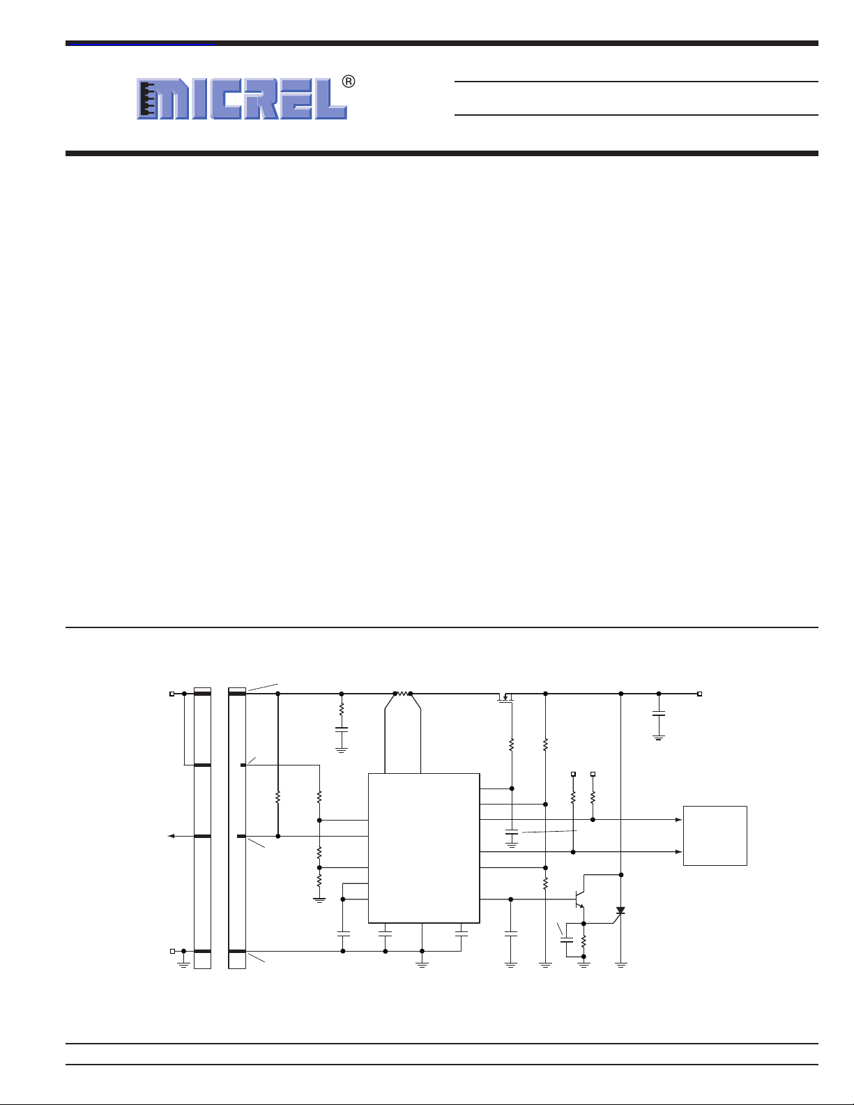
T ypical Application
(PowerPAK
/POR
FB
283
Q1
Si7884DP
14
11
10
5
7
1
C6
0.01µF
TM
SO-8)
*R6
10Ω
R7
127kΩ
1%
R10
47kΩ
R8
16.2kΩ
1%
C7
0.033µF
µ
s
V
LOGIC
C2
0.022µF
R11
47kΩ
Q2
2N4401
**R9
180Ω
C
LOAD
220µF
Output Signal
(Power Good)
Power-On Reset
Output
Q3
TCR22-4
V
OUT
12V@5A
PWRGD
LOGIC
CONTROLLER
/RESET
34
C1
µ
F
1
16 15
4
ON
6
/FAULT
9
OV
12
COMP—
13
REF
CPOR
C4
µ
F
0.1
R
SENSE
0.007Ω
2%
12
SENSEVCC
MIC2085
GATE
COMP+
COMPOUT
CRWBR
GND
CFILTER
C5
8200pF
POR/START-UP DELAY = 60ms
Circuit-Breaker Response Time = 500
*R6 is an optional component used for noise filtering
**R9 needed when using a sensitive gate SCR
V
12V
/FAULT
GND
IN
Backplane
Connector
PCB Edge
Connector
(or Short)
Long
Pin
Short
Pin
R5
47kΩ
Medium
Pin
Long
Pin
R2
100kΩ
1%
R3
1.82kΩ
1%
R4
10kΩ
1%
Overvoltage (Input) = 13.3V
Undervoltage Lockout = 10.8V
Undervoltage (Output) &
Power-Good (Output) = 11.4V
R1
3.3Ω
C3
µ
F
0.1
InfiniBand is a trademark of InfiniBand Trade Association
PowerPAK is a trademark of Vishay Intertechnology Inc.
Micrel, Inc. • 1849 Fortune Drive • San Jose, CA 95131 • USA • tel + 1 (408) 944-0800 • fax + 1 (408) 944-0970 • http://www.micrel.com
January 2004 1 M0235-121903
MIC2085/2086 Micrel
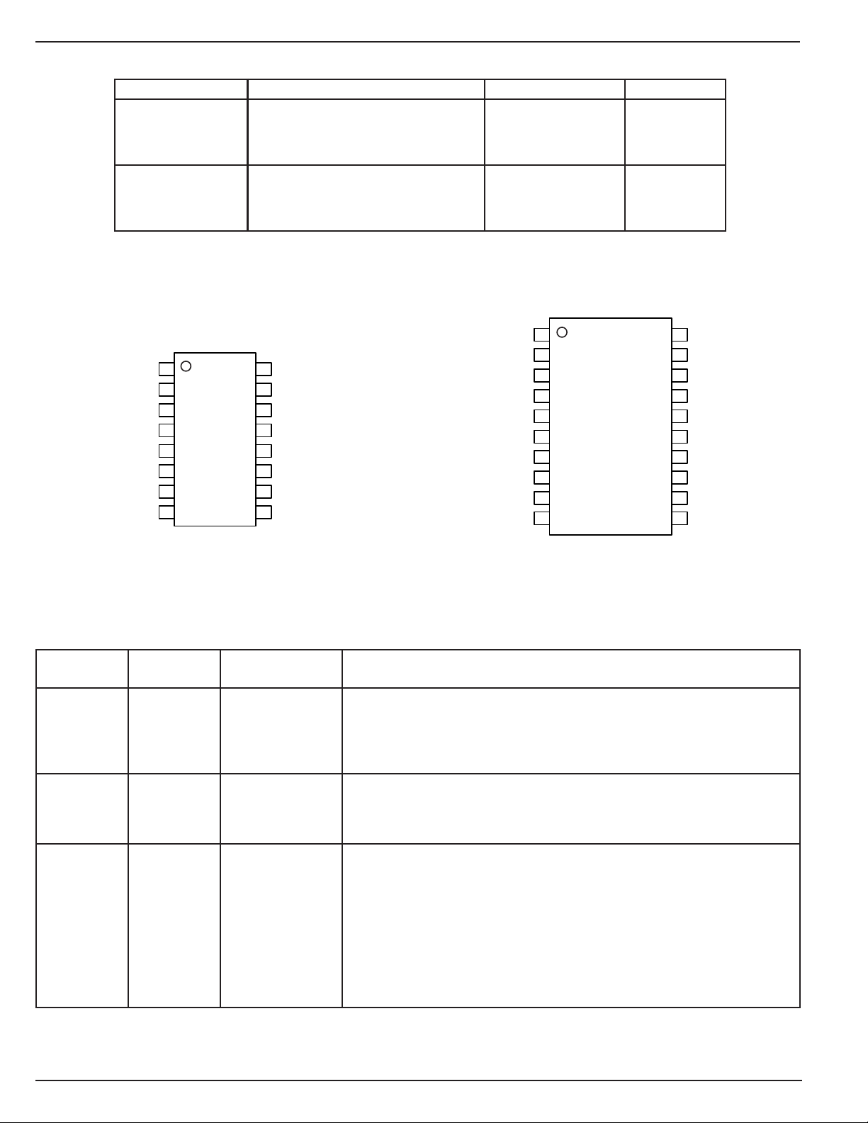
Ordering Information
Part Number Fast Circuit Breaker Threshold Discharge Output Package
MIC2085-xBQS x = J, 95mV NA 16-pin QSOP
x = K, 150mV*
x = L, 200mV*
x = M, Off
MIC2086-xBQS x = J, 95mV Yes 20-pin QSOP
x = K, 150mV*
x = L, 200mV*
x = M, Off
*Contact factory for availability.
Pin Configuration
CFILTER
CPOR
ON
/POR
/FAULT
FB
GND
1CRWBR
1CRWBR
2
3
4
5
6
7
8
16 VCC
SENSE
15
GATE
14
REF
13
COMP–
12
COMP+
11
COMPOUT
10
OV
9
CFILTER
PWRGD
CPOR
ON
/POR
/FAULT
FB
GND
GND
2
3
4
5
6
7
8
9
10
20 VCC
VCC
19
SENSE
18
GATE
17
REF
16
DIS
15
COMP–
14
COMP+
13
COMPOUT
12
OV
11
MIC2085
16-Pin QSOP (QS)
MIC2086
20-Pin QSOP (QS)
Pin Description
Pin Number Pin Number Pin Name Pin Function
MIC2086 MIC2085
1 1 CRWBR Overvoltage Timer and Crowbar Circuit Trigger: A capacitor connected to
this pin sets the timer duration for which an overvoltage condition will trigger
an external crowbar circuit. This timer begins when the OV input rises above
its threshold as an internal 45µA current source charges the capacitor. Once
the voltage reaches 470mV, the current increases to 1.5mA.
2 2 CFILTER Current Limit Response Timer: A capacitor connected to this pin defines the
period of time (t
fault condition and trip the circuit breaker. If no capacitor is connected, then
t
OCSLOW
OCSLOW
defaults to 5µs.
3 3 CPOR Power-On Reset Timer: A capacitor connected between this pin and ground
sets the start-up delay (t
VCC rises above the UVLO threshold, the capacitor connected to CPOR
begins to charge. When the voltage at CPOR crosses 1.24V, the start-up
threshold (V
C
POR
above V
CPOR rises above the power-on reset delay threshold (VTH), the timer
START
is immediately discharged to ground. When the voltage at FB rises
, capacitor C
FB
resets by pulling CPOR to ground, and /POR is deasserted.
If C
= 0, then t
POR
) in which an overcurrent event must last to signal a
) and the power-on reset interval (t
START
), a start cycle is initiated if ON is asserted while capacitor
begins to charge again. When the voltage at
POR
defaults to 20µs.
START
POR
). When
M0235-121903 2 January 2004
MIC2085/2086 Micrel
Pin Description (Cont.)
Pin Number Pin Number Pin Name Pin Function
MIC2086 MIC2085
4 4 ON ON Input: Active high. The ON pin, an input to a Schmitt-triggered compara-
tor used to enable/disable the controller, is compared to a VTH reference
with 100mV of hysteresis. Once a logic high is applied to the ON pin
> 1.24V), a start-up sequence is initiated as the GATE pin starts
(V
ON
ramping up towards its final operating voltage. When the ON pin receives a
low logic signal (V
high if VCC is above the UVLO threshold. ON must be low for at least 20µs
in order to initiate a start-up sequence. Additionally, toggling the ON pin
LOW to HIGH resets the circuit breaker.
5 5 /POR Power-On Reset Output: Open drain N-Channel device, active low. This pin
remains asserted during start-up until a time period t
voltage rises above the power-good threshold (V
C
determines t
POR
at the FB pin, /POR is asserted for a minimum of one timing cycle, t
/POR pin has a weak pull-up to VCC.
6 N/A PWRGD Power-Good Output: Open drain N-Channel device, active high. When the
voltage at the FB pin is lower than 1.24V, the PWRGD output is held low.
When the voltage at the FB pin is higher than 1.24V, then PWRGD is
asserted. A pull-up resistor connected to this pin and to VCC will pull the
output up to VCC. The PWRGD pin has a weak pull-up to VCC.
7 6 /FAULT Circuit Breaker Fault Status Output: Open drain N-Channel device, active
low. The /FAULT pin is asserted when the circuit breaker trips due to an
overcurrent condition. Also, this pin indicates undervoltage lockout and
overvoltage fault conditions. The /FAULT pin has a weak pull-up to VCC.
8 7 FB Power-Good Threshold Input: This input is internally compared to a 1.24V
reference with 3mV of hysteresis. An external resistive divider may be used
to set the voltage at this pin. If this input momentarily goes below 1.24V,
then /POR is activated for one timing cycle, t
undervoltage condition. The /POR signal de-asserts one timing cycle after
the FB pin exceeds the power-good threshold by 3mV. A 5µs filter on this pin
prevents glitches from inadvertently activating this signal.
9,10 8 GND Ground Connection: Tie to analog ground.
11 9 OV OV Input: When the voltage on OV exceeds its trip threshold, the GATE pin
is pulled low and the CRWBR timer starts. If OV remains above its threshold
long enough for CRWBR to reach its trip threshold, the circuit breaker is
tripped. Otherwise, the GATE pin begins to ramp up one POR timing cycle
after OV drops below its trip threshold.
12 10 COMPOUT Uncommitted Comparator’s Open Drain Output.
13 11 COMP+ Comparator’s Non-Inverting Input.
14 12 COMP- Comparator’s Inverting Input.
15 NA DIS Discharge Output: When the MIC2086 is turned off, a 550Ω internal resistor
at this output allows the discharging of any load capacitance to ground.
16 13 REF Reference Output: 1.24V nominal. Tie a 0.1µF capacitor to ground to ensure
stability.
17 14 GATE Gate Drive Output: Connects to the gate of an external N-Channel
MOSFET. An internal clamp ensures that no more than 13V is applied
between the GATE pin and the source of the external MOSFET. The GATE
pin is immediately brought low when either the circuit breaker trips or an
undervoltage lockout condition occurs.
< 1.14V), the GATE pin is grounded and /FAULT is
ON
after the FB pin
POR
). The timing capacitor
. When an output undervoltage condition is detected
POR
FB
, indicating an output
POR
POR
. The
January 2004 3 M0235-121903

MIC2085/2086 Micrel
Pin Description (Cont.)
Pin Number Pin Number Pin Name Pin Function
MIC2086 MIC2085
18 15 SENSE Circuit Breaker Sense Input: A resistor between this pin and VCC sets the
current limit threshold. Whenever the voltage across the sense resistor
exceeds the slow trip current limit threshold (V
is adjusted to ensure a constant load current. If V
exceeded for longer than time period t
OCSLOW
TRIPSLOW
, then the circuit breaker is
tripped and the GATE pin is immediately pulled low. If the voltage across the
sense resistor exceeds the fast trip circuit breaker threshold, V
any point due to fast, high amplitude power supply faults, then the GATE pin
is immediately brought low without delay. To disable the circuit breaker, the
SENSE and VCC pins can be tied together.
The default V
TRIPFAST
are available: 150mV, 200mV, or OFF(V
factory for availability of other options.
for either device is 95mV. Other fast trip thresholds
TRIPFAST
19,20 16 VCC Positive Supply Input: 2.3V to 16.5V. The GATE pin is held low by an
internal undervoltage lockout circuit until VCC exceeds a threshold of 2.18V.
If VCC exceeds 16.5V, an internal shunt regulator protects the chip from
VCC and SENSE pin voltages up to 33V.
), the GATE voltage
TRIPSLOW
(48mV) is
TRIPFAST
, at
disabled). Please contact
M0235-121903 4 January 2004

MIC2085/2086 Micrel
Absolute Maximum Ratings
(1)
(All voltages are referred to GND)
Supply Voltage (VCC) ..................................... –0.3V to 33V
SENSE Pin..........................................–0.3V to VCC + 0.3V
GATE Pin ....................................................... –0.3V to 22V
ON, DIS, /POR, PWRGD, /FAULT,
COMP+, COMP–, COMPOUT ....................... –0.3V to 20V
CRWBR, FB, OV, REF..................................... –0.3V to 6V
Maximum Currents
Digital Output Pins .....................................................10mA
(/POR, /FAULT, PWRGD, COMPOUT)
DIS Pin .......................................................................30mA
ESD Rating:
Human Body Model...................................................2kV
Machine Model........................................................200V
Operating Ratings
Supply Voltage (VCC) .................................... 2.3V to 16.5V
Operating Temperature Range .................. –40°C to +85°C
Junction Temperature (TJ) ........................................ 125°C
Package Thermal Resistance R
16-pin QSOP.....................................................112°C/W
20-pin QSOP.......................................................91°C/W
(2)
θ(J-A)
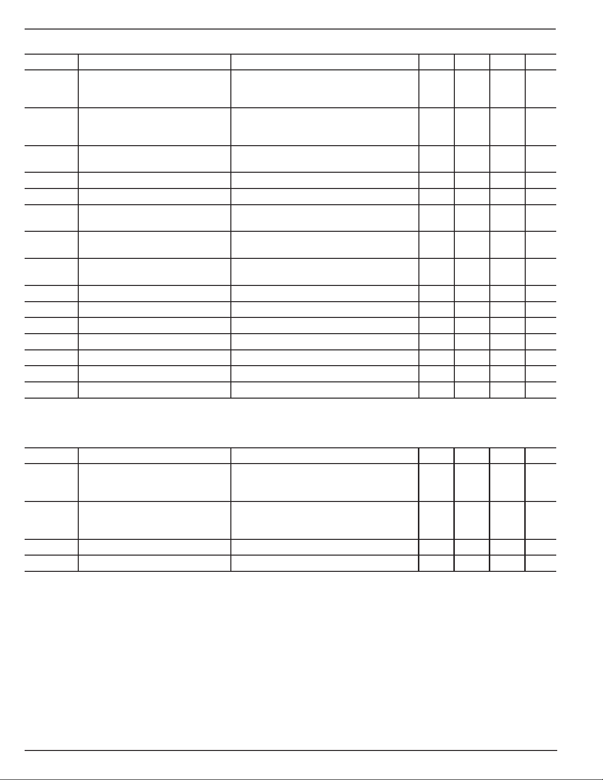
Electrical Characteristics
(3)
VCC = 5.0V, TA = 25°C unless otherwise noted. Bold indicates specifications over the full operating temperature range of –40°C to +85°C.
Symbol Parameter Condition Min Typ Max Units
V
CC
I
CC
V
UV
V
UVHYST
V
FB
V
FBHYST
V
OV
∆V
OV
V
OVHYST
I
OV
V
TH
I
CPOR
Supply Voltage 2.3 16.5 V
Supply Current 1.6 2.5 mA
Undervoltage Lockout Threshold VCC rising 2.05 2.18 2.28 V
VCC falling 1.85 2.0 2.10 V
UV Lockout Hysteresis 180 mV
FB (Power-Good) Threshold Voltage FB rising 1.19 1.24 1.29 V
FB Hysteresis 3mV
OV Pin Threshold Voltage OV pin rising 1.19 1.24 1.29 mV
OV Pin Threshold Voltage 2.3V < VCC < 16.5V 5 15 mV
Line Regulation
OV Pin Hysteresis 3mV
OV Pin Current 0.2 µA
POR Delay and Overcurrent (CFILTER) V
Timer Threshold
CPOR
, V
CFILTER
rising 1.19 1.24 1.29 V
Power-On Reset Timer Current Timer on –2.5 –2.0 –1.5 µA
Timer off 5 mA
I
TIMER
Current Limit /Overcurrent Timer on –30 –20 –15 µA
Timer Current (CFILTER) Timer off 2.5 mA
V
∆V
I
CR
V
CR
CR
TRIP
CRWBR Pin Threshold Voltage 2.3V < VCC < 16.5V 445 470 495 mV
CRWBR Pin Threshold Voltage 2.3V < VCC < 16.5V 4 15 mV
Line Regulation
CRWBR Pin Current CRWBR On, V
CRWBR On, V
CRWBR Off, V
Circuit Breaker Trip Voltage V
(Current Limit Threshold) 2.3V ≤ V
TRIP
= VCC –V
≤ 16.5V V
CC
= 0V –60 –45 –30 µA
CRWBR
= 2.1V –1.5 –1.0 mA
CRWBR
= 1.5V 3.3 mA
CRWBR
SENSE
V
TRIPSLOW
TRIPFAST
x = K 150 mV
x = J 80 95 110 mV
40 48 55 mV
x = L 200 mV
V
GS
External Gate Drive V
GATE
– V
CC
VCC < 3V 4 8 9 V
5V < VCC < 9V 11 12 13 V
9V < VCC < 15.0V 4.5 21–V
CC
13 V
January 2004 5 M0235-121903
MIC2085/2086 Micrel
Electrical Characteristics (Cont.)
Symbol Parameter Condition Min Typ Max Units
I
GATE
I
GATEOFF
V
ON
V
ONHYST
I
ON
V
START
V
OL
I
PULLUP
V
REF
∆V
LNR
∆V
LDR
I
RSC
V
COS
V
CHYST
R
DIS
GATE Pin Pull-up Current Start cycle, V
=16.5V –22 –16 –8 µA
V
CC
GATE
= 0V
VCC = 2.3V –20 –14 –8 µA
GATE Pin Sink Current /FAULT = 0, V
V
= 16.5V 25 50 mA
CC
GATE
>1V
VCC = 2.3V 12 20 mA
ON Pin Threshold Voltage ON rising 1.19 1.24 1.29 V
ON falling 1.09 1.14 1.19 V
ON Pin Hysteresis 100 mV
ON Pin Input Current VON = V
Undervoltage Start-up V
Timer Threshold
/FAULT, /POR, PWRGD Output I
Voltage (PWRGD for MIC2086 only)
OUT
CC
rising 1.19 1.24 1.29 V
CPOR
= 1.6mA 0.4 V
0.5 µA
Output Signal Pull-up Current /FAULT, /POR, PWRGD = GND –20 µA
/FAULT, /POR, PWRGD, COMPOUT (PWRGD for MIC2086 only)
Reference Output Voltage I
LOAD
= 0mA; C
= 0.1µF 1.21 1.24 1.27 V
REF
Reference Line Regulation 2.3V < VCC < 16.5V 5 10 mV
Reference Load Regulation I
Reference Short-Circuit Current V
Comparator Offset Voltage VCM = V
Comparator Hysteresis VCM = V
= 1mA 2.5 7.5 mV
OUT
= 0V 3.5 mA
REF
REF
REF
–5 5 mV
3mV
Discharge Pin Resistance ON pin toggles from HI to LOW 100 550 1000 Ω
AC Electrical Characteristics
(4)
Symbol Parameter Condition Min Typ Max Units
t
OCFAST
t
OCSLOW
t
ONDLY
t
FBDLY
Notes:
1. Exceeding the absolute maximum rating may damage the device.
2. The device is not guaranteed to function outside its operating rating.
3. Specification for packaged product only.
4. Specification for packaged product only.
Fast Overcurrent Sense to GATE VCC = 5V 1 µs
Low Trip Time V
C
–V
CC
GATE
= 100mV
SENSE
= 10nF, See Figure 1
Slow Overcurrent Sense to Gate VCC = 5V 5 µs
Low Trip Time V
CC
C
FILTER
–V
= 50mV
SENSE
= 0, See Figure 1
ON Delay Filter 20 µs
FB Delay Filter 20 µs
M0235-121903 6 January 2004
MIC2085/2086 Micrel
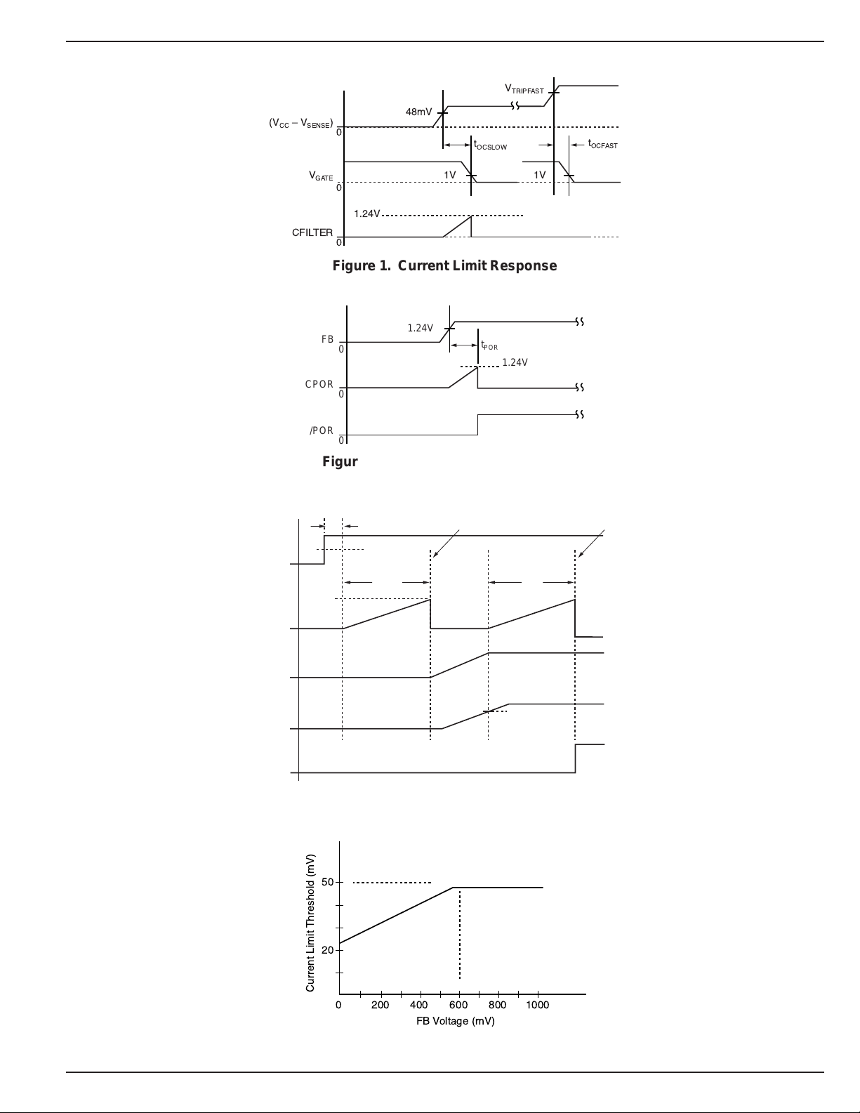
1V
48mV
V
GATE
t
OCSLOW
V
TRIPFAST
(VCCÐV
SENSE
)
t
OCFAST
1V
0
CFILTER
0
0
1.24V
Timing Diagrams
Figure 1. Current Limit Response
ON
CPOR
GATE
FB
FB
CPOR
/POR
0
0
0
1.24V
t
POR
Figure 2. Power-On Reset Response
t
ONDLY
1.24V
0
1.24V
0
0
0
Arm Fast Comparator
t
START
1.24V
Arm Slow Comparator
t
POR
1.24V
/POR
0
Figure 3. Power-On Start-Up Delay Timing
50
January 2004 7 M0235-121903
20
Current Limit Threshold (mV)
0
600 800 1000
400200
FB Voltage (mV)
Figure 4. Foldback Current Limit Response
MIC2085/2086 Micrel
g
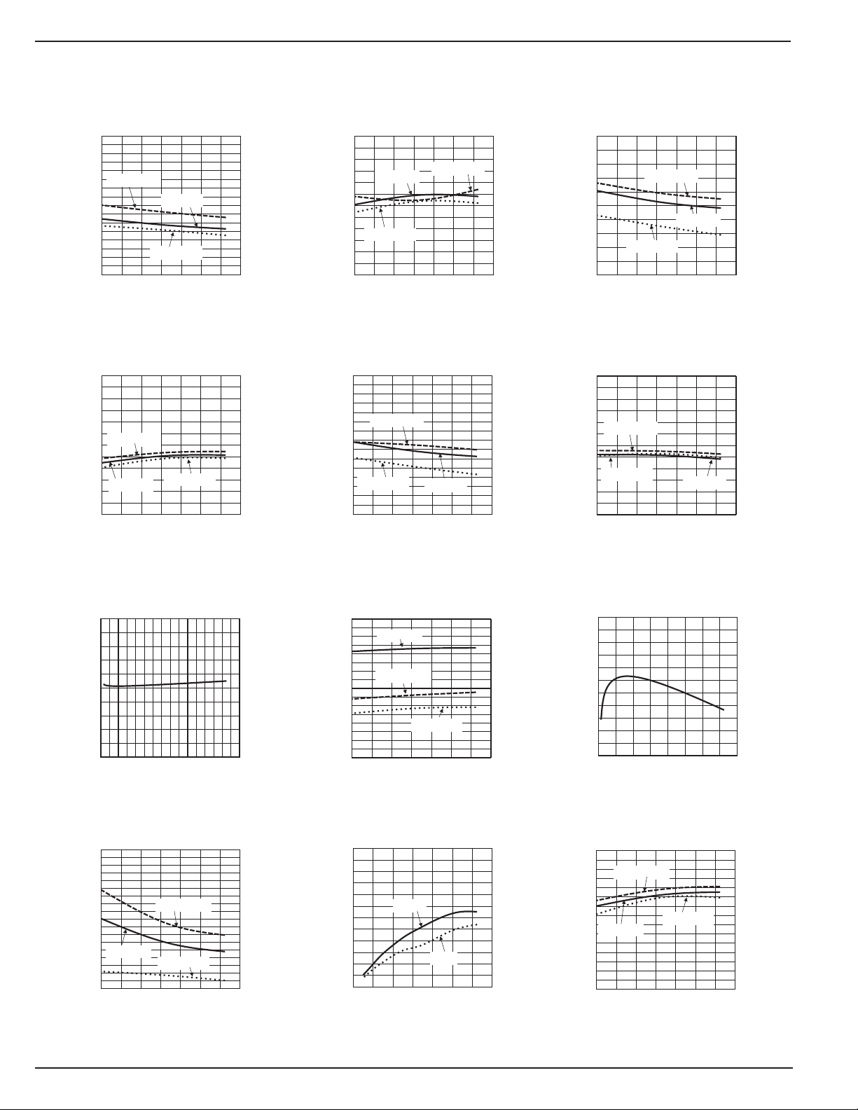
Typical Characteristics
Supply Current
4.0
vs. Temperature
3.5
3.0
V
= 16.5V
CC
2.5
2.0
VCC= 5V
1.5
1.0
SUPPLY CURRENT (mA)
0.5
0.0
-40 -20 0 20 40 60 80 100
Overcurrent Timer Current
34
VCC= 2.3V
TEMPERATURE (°C)
vs. Temperature
30
26
(µA)
VCC= 16.5V
22
TIMER
I
18
VCC= 5V
14
10
-40 -20 0 20 40 60 80 100
VCC= 2.3V
TEMPERATURE (°C)
Power-On Reset Timer Current
vs. Temperature
2.6
(µA)
CPOR
I
2.4
2.2
2.0
1.8
VCC= 5V
VCC= 2.3V
VCC= 16.5V
1.6
1.4
-40 -20 0 20 40 60 80 100
TEMPERATURE (°C)
Overcurrent Timer (Off) Current
vs. Temperature
5
4
VCC= 16.5V
3
(mA)
2
TIMER
I
VCC= 2.3V
1
0
-40 -20 0 20 40 60 80 100
TEMPERATURE (°C)
VCC= 5V
Power-On Reset Timer (Off) Current
10
vs. Temperature
9
(mA)
I
CPOR
8
7
6
5
4
3
2
VCC= 16.5V
VCC= 5V
VCC= 2.3V
1
0
-40 -20 0 20 40 60 80 100
TEMPERATURE (°C)
Gate Pull-Up Current
vs. Temperature
30
25
20
VCC= 16.5V
(µA)
15
GATE
I
10
VCC= 2.3V
5
0
-40 -20 0 20 40 60 80 100
TEMPERATURE (°C)
VCC= 5V
Gate Pull-Up Current
vs. V
25
20
15
(A)
10
GATE
I
5
0
2 4 6 8 10 12 14 16 18
Gate Sink Current
100
vs. Temperature
CC
(V)
V
CC
90
80
(mA)
70
60
VCC= 16.5V
50
GATEOFF
40
I
VCC= 5V
30
VCC= 2.3V
20
10
-40 -20 0 20 40 60 80 100
TEMPERATURE (°C)
External Gate Drive
vs. Temperature
16
VCC= 5V
14
12
10
8
6
4
VCC= 16.5V
VCC= 2.3V
(V)
GS
V
2
0
-40 -20 0 20 40 60 80 100
TEMPERATURE (°C)
Gate Sink Current
600
vs. Gate Volta
500
400
(mA)
300
GATEOFF
200
I
100
0
02468101214
12V
V
CC
GATE
5V
CC
(V)
External Gate Drive
vs. V
22
20
18
16
14
(V)
12
GS
10
V
8
6
4
2
0
2 4 6 8 10 12 14 16 18
POR Delay/Overcurrent
e
(mV)
V
TH
1.25
1.24
1.23
1.22
1.21
1.20
Timer Threshold
vs. Temperature
VCC= 16.5V
VCC= 5V
-40 -20 0 20 40 60 80 100
TEMPERATURE (°C)
CC
(V)
V
CC
VCC= 2.3V
M0235-121903 8 January 2004
MIC2085/2086 Micrel
1.7
1.8
1.9
2.0
2.1
2.2
2.3
2.4
2.5
-40 -20 0 20 40 60 80 100
UVLO THRESHOLD (V)
TEMPERATURE (°C)
10
14
18
22
26
-40 -20 0 20 40 60 80 100
I
PULLUP
(µA)
TEMPERATURE (°C)
Output Signal Pull-Up Current
vs. Temperature
VCC= 16.5V
VCC= 2.3V
VCC= 5V
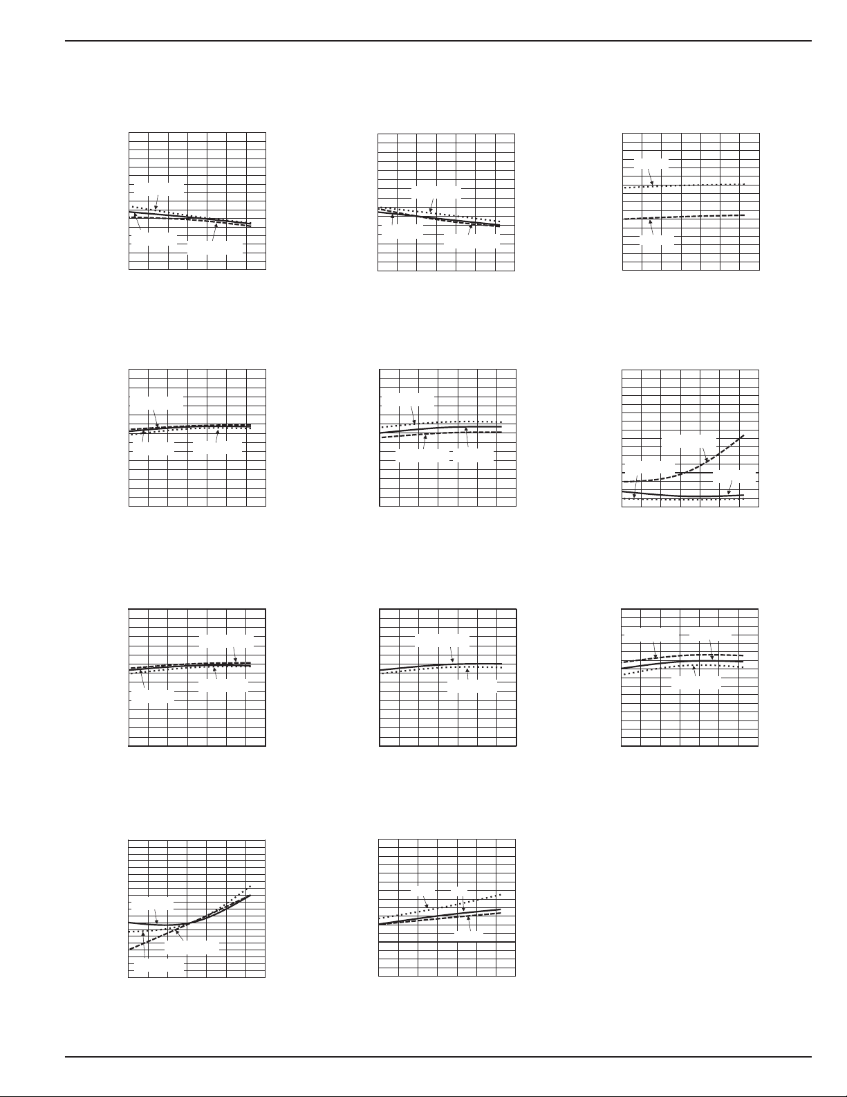
Typical Characteristics
Current Limit Threshold
(Fast Trip)
120
115
110
105
(mV)
100
TRIPFAST
V
1.30
1.25
1.20
ON THRESHOLD (V)
1.15
vs. Temperature
VCC= 2.3V
95
90
VCC= 5V
85
80
-40 -20 0 20 40 60 80 100
ON Pin Threshold (Rising)
VCC= 16.5V
VCC= 5V
-40 -20 0 20 40 60 80 100
VCC= 16.5V
TEMPERATURE (°C)
vs. Temperature
VCC= 2.3V
TEMPERATURE (°C)
Current Limit Threshold
(Slow Trip)
vs. Temperature
55
53
(mV)
51
49
TRIPSLOW
V
47
45
-40 -20 0 20 40 60 80 100
1.20
1.15
1.10
ON THRESHOLD (V)
1.05
VCC= 2.3V
VCC= 5V
TEMPERATURE (°C)
ON Pin Threshold (Falling)
vs. Temperature
VCC= 2.3V
VCC= 16.5V
-40 -20 0 20 40 60 80 100
VCC= 16.5V
VCC= 5V
TEMPERATURE (°C)
UVLO Threshold
vs. Temperature
UVLO+
UVLO–
ON Pin Input Current
vs. Temperature
40
35
30
25
20
15
10
5
ON PIN INPUT CURRENT (nA)
0
-40 -20 0 20 40 60 80 100
VCC= 16.5V
VCC= 2.3V
TEMPERATURE (°C)
VCC= 5V
FB (Power-Good) Threshold
1.30
1.25
1.20
FB THRESHOLD (V)
1.15
-40 -20 0 20 40 60 80 100
Comparator Offset Voltage
0.5
0.4
0.3
January 2004 9 M0235-121903
0.2
0.1
0.0
-40 -20 0 20 40 60 80 100
COMPARATOR OFFSET VOLTAGE (V)
vs. Temperature
VCC= 5V
TEMPERATURE (°C)
vs. Temperature
VCC= 5V
VCC= 16.5V
VCC= 2.3V
TEMPERATURE (°C)
VCC= 16.5V
VCC= 2.3V
Overvoltage Pin Threshold
1.30
1.25
1.20
1.15
OVERVOLTAGE PIN THRESHOLD (V)
1000
900
800
700
(Ω)
600
DIS
500
R
400
300
200
vs. Temperature
VCC= 16.5V
VCC= 2.3V
-40 -20 0 20 40 60 80 100
TEMPERATURE (°C)
Discharge Pin Resistance
vs. Temperature
2.3V
5V
16.5V
-40 -20 0 20 40 60 80 100
TEMPERATURE (°C)
 Loading...