

Page 1

MiCOM P631
Transformer Differential Protection Device
P631/EN M/R-11-C
Version P631 -310 -409/410 -650
Technical Manual
Page 2

Page 3

General Note on the PDF Version of this Technical Manual
All entries in the Table of Contents and all cross-references to other sections,
figures etc. in green letters are hyperlinks, i.e. by a single mouse click on the
reference one can navigate directly to the referenced part of the manual.
In the Adobe Reader (or the Acrobat Pro), one can return back to the previous
view by using the menu point View / Page Navigation / Previous View (keyboard
shortcut: ALT + Left cursor key). (It might be necessary to do this several times,
if the view at the target location has also been changed (e.g. by scrolling or
changing the zoom setting).
Page 4

Page 5

Warning!
When electrical equipment is in operation dangerous voltage will be present in
⚫
certain parts of the equipment. Failure to observe warning notices, incorrect
use or improper use may endanger personnel and equipment and cause
personal injury or physical damage.
Before working in the terminal strip area, the P631 must be isolated. Where
stranded conductors are used, insulated crimped wire end ferrules must be
employed.
The signals MAIN: Blocked/faulty and SFMON: Warning (LED)
(permanently assigned to the LEDs labeled OUT OF SERVICE and ALARM) can
be assigned to output relays to indicate the health of the P631. Schneider
Electric strongly recommends that these output relays are hardwired into the
substation's automation system, for alarm purposes.
Any modifications to this P631 must be in accordance with the manual. If any
other modification is made without the express permission of Schneider
Electric, it will invalidate the warranty, and may render the product unsafe.
Proper and safe operation of this P631 depends on appropriate shipping and
handling, proper storage, installation and commissioning, and on careful
operation, maintenance and servicing.
For this reason only qualified personnel may work on or operate this P631.
The User should be familiar with the warnings in the Safety Guide
(SFTY/4LM/J11 or later version), with the warnings in Chapter 5, (p. 5-1),
Chapter 10, (p. 10-1), Chapter 11, (p. 11-1) and Chapter 12, (p. 12-1)
and with the content of Chapter 14, (p. 14-1), before working on the
equipment. If the warnings are disregarded, it will invalidate the warranty, and
may render the product unsafe.
Installation of the DHMI:
A protective conductor (ground/earth) of at least 1.5 mm² (US: AWG14 or
thicker) must be connected to the DHMI protective conductor terminal to link
the DHMI and the main relay case; these must be located within the same
substation.
To avoid the risk of electric shock the DHMI communication cable must not be
in contact with hazardous live parts.
The DHMI communication cable must not be routed or placed alongside highvoltage cables or connections. Currents can be induced in the cable which
may result in electromagnetic interference.
Qualified Personnel
are individuals who
are familiar with the installation, commissioning and operation of the P631
●
and of the system to which it is being connected;
are able to perform switching operations in accordance with safety
●
engineering standards and are authorized to energize and de-energize
equipment and to isolate, ground and label it;
are trained in the care and use of safety apparatus in accordance with
●
safety engineering standards;
are trained in emergency procedures (first aid).
●
Page 6

Note
This operating manual gives instructions for installation, commissioning and
operation of the P631. However, the manual cannot cover all conceivable
circumstances or include detailed information on all topics. In the event of
questions or specific problems, do not take any action without proper
authorization. Contact the appropriate technical sales office of Schneider Electric
and request the necessary information.
Any agreements, commitments, and legal relationships and any obligations on
the part of Schneider Electric, including settlement of warranties, result solely
from the applicable purchase contract, which is not affected by the contents of
the operating manual.
Page 7

Changes after going to press
Page 8

Page 9

P631
TABLE OF CONTENTS
1 APPLICATION AND SCOPE ................................................................................... 1-1
1.1 Overview - P631 ..........................................................................................................1-1
1.2 Including Function Groups in the Configuration ..........................................................1-3
1.3 Overview of Function Groups - Part 1 ......................................................................... 1-4
1.4 Overview of Function Groups - Part 2 ......................................................................... 1-6
1.5 Design .........................................................................................................................1-8
1.6 Configurable Function Keys ........................................................................................ 1-9
1.7 Inputs and Outputs ................................................................................................... 1-10
1.8 Control and Display ...................................................................................................1-11
1.9 Information Interfaces ...............................................................................................1-12
2 TECHNICAL DATA ................................................................................................2-1
2.1 Conformity ..................................................................................................................2-1
2.2 General Data ...............................................................................................................2-2
2.2.1 General Device Data ..................................................................................................................................... 2-2
2.3 Tests ...........................................................................................................................2-4
2.3.1 Type Tests .....................................................................................................................................................2-4
2.3.2 Routine Tests .................................................................................................................................................2-7
2.4 Environmental Conditions ...........................................................................................2-9
2.5 Inputs and Outputs ................................................................................................... 2-10
2.5.1 Current Measuring Inputs ............................................................................................................................2-10
2.5.2 Binary Signal Inputs .....................................................................................................................................2-11
2.5.3 IRIG‑B Interface ........................................................................................................................................... 2-12
2.5.4 Direct Current Input .....................................................................................................................................2-12
2.5.5 Resistance Thermometer ............................................................................................................................ 2-12
2.5.6 Direct Current Output ..................................................................................................................................2-12
2.5.7 Output Relays ..............................................................................................................................................2-13
2.5.8 BCD Measured Data Output ........................................................................................................................ 2-13
2.6 Interfaces ..................................................................................................................2-14
2.6.1 Local Control Panel ......................................................................................................................................2-14
2.6.2 PC Interface .................................................................................................................................................2-14
2.6.3 Serial Communication Interface .................................................................................................................. 2-14
2.6.4 IEC Communication Interface ......................................................................................................................2-15
2.6.5 IRIG‑B Interface ........................................................................................................................................... 2-15
2.7 Information Output ................................................................................................... 2-16
2.8 Settings – Typical Characteristic Data .......................................................................2-17
2.8.1 Main Function ..............................................................................................................................................2-17
2.8.2 Differential Protection ..................................................................................................................................2-17
2.8.3 Definite-Time and Inverse-Time Overcurrent Protection ............................................................................. 2-17
2.9 Deviations .................................................................................................................2-18
2.9.1 Deviations of the Operate Values ................................................................................................................2-18
2.9.2 Deviations of the Timer Stages ................................................................................................................... 2-19
2.9.3 Deviations of Measured Data Acquisition ....................................................................................................2-20
2.10 Resolution of the Fault Data Acquisition ...................................................................2-21
2.10.1 Time Resolution ...........................................................................................................................................2-21
2.10.2 Currents .......................................................................................................................................................2-21
2.10.3 Voltage ........................................................................................................................................................2-21
2.11 Recording Functions ................................................................................................. 2-22
P631/EN M/R-11-C // P631-310-650 1
Page 10

P631
2.11.1 Organization of the Recording Memories .................................................................................................... 2-22
Table of Contents
2.12 Power Supply ............................................................................................................ 2-24
2.13 Current Transformer Specifications .......................................................................... 2-25
2.13.1 Symbols .......................................................................................................................................................2-25
2.13.2 General Equations .......................................................................................................................................2-26
2.13.3 Transformer Differential Protection .............................................................................................................2-27
3 OPERATION .........................................................................................................3-1
3.1 Modular Structure .......................................................................................................3-1
3.2 Operator-Machine Communication ............................................................................. 3-3
3.3 Configuration of the Measured Value Panels (Function Group LOC) ........................... 3-4
3.3.1 Operation Panel .............................................................................................................................................3-5
3.3.2 Fault Panel .....................................................................................................................................................3-6
3.3.3 Overload Panel ..............................................................................................................................................3-7
3.3.4 Configurable Clear Key ..................................................................................................................................3-7
3.4 Serial Interfaces ..........................................................................................................3-8
3.4.1 PC Interface (Function Group PC) .................................................................................................................. 3-9
3.4.2 Communication Interface 1 (Function Group COMM1) ................................................................................ 3-10
3.4.3 Communication Interface 2 (Function Group COMM2) ................................................................................ 3-19
3.4.4 Communication Interface IEC 61850 (Function Groups IEC, GOOSE and GSSE) ..........................................3-21
3.5 IRIG-B Clock Synchronization (Function Group IRIGB) ...............................................3-33
3.6 Configurable Function Keys (Function Group F_KEY) ................................................ 3-34
3.7 Configuration and Operating Mode of the Binary Inputs (Function Group INP) .........3-36
3.8 Measured Data Input (Function Group MEASI) ..........................................................3-38
3.8.1 Direct Current Input on the Analog (I/O) Module Y ...................................................................................... 3-39
3.8.2 Input for Connection of a Resistance Thermometer .................................................................................... 3-42
3.9 Configuration, Operating Mode, and Blocking of the Output Relays (Function Group
OUTP) ........................................................................................................................3-44
3.10 Measured Data Output (Function Group MEASO) ......................................................3-47
3.10.1 General Settings ..........................................................................................................................................3-47
3.10.2 BCD Measured Data Output ........................................................................................................................ 3-49
3.10.3 Analog Measured Data Output .................................................................................................................... 3-52
3.10.4 Output of “External” Measured Data ...........................................................................................................3-58
3.11 Configuration and Operating Mode of the LED Indicators (Function Group LED) ...... 3-59
3.11.1 Configuring the LED Indicators ....................................................................................................................3-59
3.11.2 Layout of the LED Indicators ........................................................................................................................3-59
3.11.3 Operating Mode of the LED Indicators .........................................................................................................3-60
3.12 Main Functions of the P631 (Function Group MAIN) ..................................................3-62
3.12.1 Conditioning of the Measured Values ..........................................................................................................3-62
3.12.2 Phase Reversal Function ..............................................................................................................................3-65
3.12.3 Operating Data Measurement ..................................................................................................................... 3-67
3.12.4 Configuring and Enabling the Device Functions .......................................................................................... 3-74
3.12.5 Activation of “Dynamic Parameters” ...........................................................................................................3-76
3.12.6 Multiple Blocking ......................................................................................................................................... 3-77
3.12.7 Multiple Signaling of the Measuring Circuit Monitoring Function .................................................................3-78
3.12.8 Blocked/Faulty .............................................................................................................................................3-79
3.12.9 Starting Signals and Tripping Logic .............................................................................................................3-79
3.12.10 Time Tagging and Clock Synchronization ....................................................................................................3-82
3.12.11 Resetting Actions .........................................................................................................................................3-84
3.12.12 Assigning Communications Interfaces to Physical Communications Channels ............................................3-87
3.12.13 Test Mode ....................................................................................................................................................3-88
3.13 Parameter Subset Selection (Function Group PSS) ................................................... 3-89
2 P631/EN M/R-11-C // P631-310-650
Page 11

Table of Contents
3.14 Self-Monitoring (Function Group SFMON) ..................................................................3-91
3.14.1 Tests During Start-up .................................................................................................................................. 3-91
3.14.2 Cyclic Tests ..................................................................................................................................................3-91
3.14.3 Signals .........................................................................................................................................................3-91
3.14.4 Device Response .........................................................................................................................................3-92
3.14.5 Monitoring Signal Memory ...........................................................................................................................3-93
3.14.6 Monitoring Signal Memory Time Tag ...........................................................................................................3-93
3.15 Operating Data Recording (Function Group OP_RC) ................................................. 3-94
3.16 Monitoring Signal Recording (Function Group MT_RC) ..............................................3-95
3.17 Overload Data Acquisition (Function Group OL_DA) ................................................. 3-96
3.17.1 Overload Duration .......................................................................................................................................3-96
3.17.2 Acquiring Measured Overload Data from the Thermal Overload Protection ................................................3-97
3.18 Overload Recording (Function Group OL_RC) ............................................................3-98
3.18.1 Start of Overload Recording ........................................................................................................................3-98
3.18.2 Counting Overload Events ...........................................................................................................................3-98
3.18.3 Time Tagging ...............................................................................................................................................3-98
3.18.4 Overload Logging ........................................................................................................................................ 3-99
3.19 Fault Data Acquisition (Function Group FT_DA) ...................................................... 3-100
3.19.1 Running Time and Fault Duration ..............................................................................................................3-100
3.19.2 Fault Data Acquisition Time .......................................................................................................................3-100
3.19.3 Acquisition of the Fault Currents ............................................................................................................... 3-102
3.19.4 Acquisition of the Differential and Restraining Currents ............................................................................3-102
3.19.5 Fault Data Reset ........................................................................................................................................3-103
3.20 Fault Recording (Function Group FT_RC) ................................................................ 3-104
3.20.1 Start of Fault Recording .............................................................................................................................3-104
3.20.2 Fault Counting ...........................................................................................................................................3-105
3.20.3 Time Tagging .............................................................................................................................................3-105
3.20.4 Fault Recordings ........................................................................................................................................3-106
3.20.5 Fault Value Recording ............................................................................................................................... 3-107
3.21 Differential Protection (Function Group DIFF) ......................................................... 3-109
3.21.1 Enabling or Disabling Differential Protection .............................................................................................3-109
3.21.2 Amplitude Matching ...................................................................................................................................3-110
3.21.3 Vector Group Matching ..............................................................................................................................3-113
3.21.4 Zero-sequence Current Filtering ................................................................................................................3-113
3.21.5 Tripping Characteristics .............................................................................................................................3-115
3.21.6 Rapid (high-set) Differential Protection ..................................................................................................... 3-117
3.21.7 Inrush Stabilization (Harmonic Restraint) ..................................................................................................3-118
3.21.8 Saturation Discriminator ............................................................................................................................3-119
3.21.9 Overfluxing Stabilization ........................................................................................................................... 3-120
3.21.10 Measured Operating Data of Differential Protection ..................................................................................3-121
3.22 Definite-Time Overcurrent Protection (Function Groups DTOC1 and DTOC2) .........3-123
3.22.1 Enabling or Disabling DTOC Protection ......................................................................................................3-123
3.22.2 Phase Current Stages ................................................................................................................................3-124
3.22.3 Negative-Sequence Current Stages ...........................................................................................................3-126
3.22.4 Residual Current Stages ............................................................................................................................3-127
3.22.5 General Starting ........................................................................................................................................3-129
3.22.6 Counters of the DTOC Protection Function ................................................................................................3-130
3.23 Inverse-time Overcurrent Protection (Function Groups IDMT1 and IDMT2) ............ 3-131
3.23.1 Enabling or Disabling IDMT Protection .......................................................................................................3-131
3.23.2 Time-Dependent Characteristics ............................................................................................................... 3-133
3.23.3 Phase Current Stage ..................................................................................................................................3-136
3.23.4 Negative-Sequence Current Stage ............................................................................................................ 3-138
3.23.5 Residual Current Stage ..............................................................................................................................3-140
3.23.6 Hold Time ..................................................................................................................................................3-142
P631
P631/EN M/R-11-C // P631-310-650 3
Page 12

P631
3.23.7 General Starting ........................................................................................................................................3-144
3.23.8 Counters of the IDMT Protection Function .................................................................................................3-144
Table of Contents
3.24 Thermal Overload Protection (Function Group THRM1) .......................................... 3-145
3.24.1 Enabling or Disabling Thermal Overload Protection .................................................................................. 3-145
3.24.2 Readiness of Thermal Overload Protection ................................................................................................3-146
3.24.3 Tripping Characteristics .............................................................................................................................3-146
3.24.4 Coolant Temperature Acquisition .............................................................................................................. 3-147
3.24.5 Warning Signal .......................................................................................................................................... 3-148
3.25 Current Transformer Supervision (Function Group CTS) .........................................3-151
3.25.1 Hardware requirement .............................................................................................................................. 3-151
3.25.2 Enabling or Disabling the CTS Function .....................................................................................................3-151
3.25.3 Blocking CTS ..............................................................................................................................................3-151
3.25.4 Monitoring Condition ................................................................................................................................. 3-152
3.25.5 Signaling and Indication ............................................................................................................................3-153
3.25.6 Reset .........................................................................................................................................................3-154
3.25.7 Multiple Signaling from the CTS Function ..................................................................................................3-154
3.26 Measuring-Circuit Monitoring (Function Groups MCM_1 and MCM_2) ..................... 3-156
3.26.1 Enabling or Disabling Measuring-Circuit Monitoring ..................................................................................3-156
3.26.2 Measuring-Circuit Monitoring .....................................................................................................................3-156
3.26.3 Multiple Signaling from the Measuring-Circuit Monitoring Function .......................................................... 3-157
3.27 Circuit Breaker Failure Protection (Function Groups CBF_1 and CBF_2) ..................3-158
3.27.1 Assigning Transformer Ends ......................................................................................................................3-158
3.27.2 Assigning Circuit Breakers .........................................................................................................................3-158
3.27.3 Assigning the Trip Command .....................................................................................................................3-158
3.27.4 Enabling or Disabling the CBF Function .....................................................................................................3-158
3.27.5 Readiness of Circuit Breaker Protection .................................................................................................... 3-159
3.27.6 Detecting a CB Tripping .............................................................................................................................3-160
3.27.7 Current flow monitoring .............................................................................................................................3-160
3.27.8 Evaluation of CB Status Signals .................................................................................................................3-161
3.27.9 Startup Criteria ..........................................................................................................................................3-162
3.27.10 Trip Commands ......................................................................................................................................... 3-164
3.27.11 Starting Trigger ......................................................................................................................................... 3-164
3.27.12 Fault Behind CB Protection ........................................................................................................................3-165
3.27.13 CB Synchronization Supervision ................................................................................................................3-165
3.28 Limit Value Monitoring (Function Group LIMIT) .......................................................3-167
3.28.1 Enabling or Disabling the Limit Value Monitoring Function ....................................................................... 3-167
3.28.2 Monitoring the Linearized Measured DC Values ........................................................................................ 3-167
3.28.3 Monitoring the Measured Temperature Value ........................................................................................... 3-168
3.29 Limit Value Monitoring (Function Groups LIM_1 and LIM_2) ....................................3-170
3.29.1 Monitoring Minimum and Maximum Phase Currents ................................................................................. 3-170
3.30 Programmable Logic (Function Groups LOGIC and LOG_2) .....................................3-172
4 DESIGN ............................................................................................................... 4-1
4.1 Designs .......................................................................................................................4-2
4.2 Dimensional Drawings ................................................................................................ 4-4
4.2.1 Dimensional Drawings for the 40 TE Case .....................................................................................................4-4
4.2.2 Detachable HMI .............................................................................................................................................4-5
4.3 Hardware Modules ......................................................................................................4-7
5 INSTALLATION AND CONNECTION .......................................................................5-1
5.1 Unpacking and Packing ...............................................................................................5-2
5.2 Checking Nominal Data and Design Type ...................................................................5-3
5.3 Location Requirements ...............................................................................................5-4
4 P631/EN M/R-11-C // P631-310-650
Page 13

Table of Contents
5.3.1 Environmental Conditions ..............................................................................................................................5-4
5.3.2 Mechanical Conditions ...................................................................................................................................5-4
5.3.3 Electrical Conditions for Auxiliary Voltage of the Power Supply .................................................................... 5-4
5.3.4 Electromagnetic Conditions ...........................................................................................................................5-4
P631
5.4 Installation ..................................................................................................................5-5
5.5 Protective and Operational Grounding ......................................................................5-11
5.6 Connection ................................................................................................................5-12
5.6.1 Connecting Measuring and Auxiliary Circuits .............................................................................................. 5-12
5.6.2 Connecting the IRIG‑B Interface .................................................................................................................. 5-14
5.6.3 Connecting the Serial Interfaces ................................................................................................................. 5-14
5.7 Location and Connection Diagrams .......................................................................... 5-18
5.7.1 Location Diagrams P631‑409/410 ................................................................................................................5-18
5.7.2 Terminal Connection Diagrams P631‑409/410 ............................................................................................ 5-18
6 LOCAL CONTROL (HMI) ....................................................................................... 6-1
6.1 Local Control Panel (HMI) ............................................................................................6-1
6.2 Display and Keypad .................................................................................................... 6-2
6.2.1 Text Display ...................................................................................................................................................6-2
6.2.2 Display Illumination .......................................................................................................................................6-2
6.2.3 Contrast of the Display ..................................................................................................................................6-2
6.2.4 Short Description of Keys .............................................................................................................................. 6-3
6.3 Display Levels .............................................................................................................6-5
6.4 Display Panels .............................................................................................................6-6
6.5 Menu Tree and Data Points .........................................................................................6-7
6.6 List Data Points ...........................................................................................................6-8
6.7 Note Concerning the Step-by-Step Descriptions .........................................................6-9
6.8 Configurable Function Keys ...................................................................................... 6-10
6.8.1 Configuration of the Function Keys F1 to Fx ................................................................................................6-11
6.9 Changing Between Display Levels ............................................................................ 6-14
6.10 Control at Panel Level ...............................................................................................6-15
6.11 Control at the Menu Tree Level .................................................................................6-16
6.11.1 Navigation in the Menu Tree ....................................................................................................................... 6-16
6.11.2 Switching Between Address Mode and Plain Text Mode ..............................................................................6-17
6.11.3 Change-Enabling Function ...........................................................................................................................6-18
6.11.4 Changing Parameters ..................................................................................................................................6-21
6.11.5 List Parameters ........................................................................................................................................... 6-22
6.11.6 Memory Readout .........................................................................................................................................6-25
6.11.7 Resetting .....................................................................................................................................................6-28
6.11.8 Password-Protected Control Actions ............................................................................................................6-29
6.11.9 Changing the Password ...............................................................................................................................6-31
7 SETTINGS ............................................................................................................7-1
7.1 Parameters .............................................................................................................. 7-1
7.1.1 Device Identification ............................................................................................................................. 7-3
7.1.2 Configuration Parameters .................................................................................................................. 7-11
7.1.3 Function Parameters ............................................................................................................................7-71
8 INFORMATION AND CONTROL FUNCTIONS ......................................................... 8-1
8.1 Operation ................................................................................................................. 8-1
8.1.1 Cyclic Values ............................................................................................................................................ 8-2
8.1.2 Control and Testing ..............................................................................................................................8-82
8.1.3 Operating Data Recording ..................................................................................................................8-92
P631/EN M/R-11-C // P631-310-650 5
Page 14

P631
Table of Contents
8.2 Events .....................................................................................................................8-93
8.2.1 Event Counters ...................................................................................................................................... 8-93
8.2.2 Measured Event Data ...........................................................................................................................8-96
8.2.3 Event Recording .................................................................................................................................... 8-99
9 IEC 61850 SETTINGS VIA IED CONFIGURATOR ....................................................9-1
9.1 Manage IED .................................................................................................................9-2
9.2 IED Details .................................................................................................................. 9-3
9.3 Communications .........................................................................................................9-4
9.4 SNTP ........................................................................................................................... 9-5
9.4.1 General Config ...............................................................................................................................................9-5
9.4.2 External Server 1 ...........................................................................................................................................9-5
9.4.3 External Server 2 ...........................................................................................................................................9-5
9.5 Dataset Definitions ..................................................................................................... 9-6
9.6 GOOSE Publishing .......................................................................................................9-7
9.6.1 System/LLN0 ................................................................................................................................................. 9-7
9.7 GOOSE Subscribing .....................................................................................................9-9
9.7.1 Mapped Inputs ...............................................................................................................................................9-9
9.8 Report Control Blocks ............................................................................................... 9-12
9.8.1 System/LLN0 ............................................................................................................................................... 9-12
9.9 Controls .....................................................................................................................9-13
9.9.1 Control Objects ............................................................................................................................................9-13
9.9.2 Uniqueness of Control ................................................................................................................................. 9-13
9.10 Measurements .......................................................................................................... 9-15
9.11 Configurable Data Attributes .................................................................................... 9-16
9.11.1 System/LLN0 ............................................................................................................................................... 9-16
10 COMMISSIONING ...............................................................................................10-1
10.1 Safety Instructions ....................................................................................................10-1
10.2 Commissioning Tests ................................................................................................10-3
10.2.1 Preparation ..................................................................................................................................................10-3
10.2.2 Testing .........................................................................................................................................................10-5
10.2.3 Checking the Binary Signal Inputs ...............................................................................................................10-5
10.2.4 Checking the Output Relays ........................................................................................................................10-5
10.2.5 Checking the Protection Function ................................................................................................................10-5
10.2.6 Completing Commissioning .........................................................................................................................10-9
11 TROUBLESHOOTING ..........................................................................................11-1
12 MAINTENANCE .................................................................................................. 12-1
12.1 Maintenance Procedures in the Power Supply Area ..................................................12-2
12.2 Routine Functional Testing ....................................................................................... 12-3
12.3 Analog Input Circuits .................................................................................................12-4
12.4 Binary Opto Inputs ....................................................................................................12-5
12.5 Binary Outputs ..........................................................................................................12-6
12.6 Serial Interfaces ........................................................................................................12-7
13 STORAGE .......................................................................................................... 13-1
14 ACCESSORIES AND SPARE PARTS .....................................................................14-1
6 P631/EN M/R-11-C // P631-310-650
Page 15

Table of Contents
P631
15 ORDER INFORMATION .......................................................................................15-1
A1 FUNCTION GROUPS ...........................................................................................A1-1
A2 INTERNAL SIGNALS ...........................................................................................A2-1
A3 GLOSSARY ........................................................................................................A3-1
Modules ......................................................................................................................................A3-1
Symbols ......................................................................................................................................A3-1
Examples of Signal Names ......................................................................................................... A3-7
Symbols Used .............................................................................................................................A3-8
A4 TELECONTROL INTERFACES ..............................................................................A4-1
A4.1 Telecontrol Interface per EN 60870-5-101 or IEC 870-5-101 (Companion Standard)
.................................................................................................................................. A4-1
A4.1.1 Interoperability ............................................................................................................................................A4-1
A4.2 Communication Interface per IEC 60870-5-103 ........................................................A4-9
A4.2.1 Interoperability ............................................................................................................................................A4-9
A5 P631 VERSION HISTORY ................................................................................... A5-1
P631/EN M/R-11-C // P631-310-650 7
Page 16

P631
Table of Contents
8 P631/EN M/R-11-C // P631-310-650
Page 17

1 APPLICATION AND SCOPE
1.1 Overview - P631
The P631 differential protection device is intended for the fast and selective
short-circuit protection of transformers, motors, generators and other
installations with 2 windings.
P631
Fig. 1-1: P631 in 40 TE case.
The P631 provides high-speed three-system differential protection using a tripleslope characteristic and two high-set differential elements in combination with
transformer inrush restraint, overfluxing restraint and through-stabilization.
Amplitude and vector group matching is done just by entering the nominal values
of transformer windings and associated current transformers. An (optional)
overreaching current measuring circuit monitoring function will prevent
unwanted tripping by differential protection for faults in the CT's secondary
circuit.
Phase swapping allows motor / generator protection applications with enlarged
protection zones.
In addition many supplementary protective functions are incorporated in the
devices. These can be individually configured and cancelled.
The relevant protection parameters can be stored in four independent parameter
subsets in order to adapt the protection device to different operating and power
system management conditions.
During operation, the user-friendly interface makes it easy to set the device
parameters and allows safe operation of the substation by preventing nonpermissible switching operations.
These features give the user the means to adapt the P631 to the protection and
control capacity required in a specific application.
The powerful programmable logic provided by the protection device also makes
it possible to accommodate special applications.
P631/EN M/R-11-C // P631-310-650 1-1
Page 18
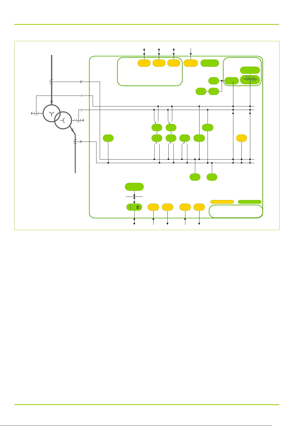
I
Y,b
I
Y,a
I
P,a
I
P,b
87
DIFF
49
THRM1
51
IDMT1
51
IDMT2
50
DTOC2
Metering
LIM_1
Overload rec.
Self Monitoring
LIM_2
Fault rec.
Communication
to SCADA / substation control / RTU / modem ...
via RS485 or Fiber optics
using IEC 60870-5-101, -103, Modbus, DNP3, Courier
resp.
via RJ45 or Fiber optics using IEC 61850
16S
COMM1
16S
COMM2
16E
IEC
CLK
IRIGB
CMD_1SIG_1
26
MEASI MEASO
Transformer Differential Protection
P631
Always availableOptional
LIMIT
50
DTOC1
50/62BF
CBF_2
50/62BF
CBF_1
MCM_2MCM_1
CTS
Recording and
Data Acquisition
LGC
LOGIC / LOG2
P631
1 Application and Scope
Fig. 1-2: Function diagram
For a list of all available function groups see the Appendix.
1-2 P631/EN M/R-11-C // P631-310-650
Page 19

1 Application and Scope
1.2 Including Function Groups in the Configuration
Functions listed in the tables in Section 1.3, (p. 1-4) are self-contained
function groups and can be individually configured or de-configured according to
the specific application requirements by using the MiCOM S1 operating program.
Unused or cancelled function groups are hidden to the user, thus simplifying the
menu of the MiCOM S1.
This concept provides a large choice of functions and makes wide-ranging
application of the protection device possible, with just one model version. On the
other hand, simple and clear parameter settings can be made.
In this way the protection and control functions can be included in or excluded
from the configuration.
Example
For example, the current transformer supervision (function group CTS)
can be included in the configuration by setting
●
CTS: Function group CTS to With
can be excluded from the configuration by setting
●
CTS: Function group CTS to Without
P631
P631/EN M/R-11-C // P631-310-650 1-3
Page 20

P631
1 Application and Scope
1.3 Overview of Function Groups - Part 1
The following tables list the function groups that can be included in or excluded
from the configuration of the P631.
✓ = Standard; (✓) = Ordering option.
Protection functions
P631ANSI IEC 61850 Function group
Abbrev. Description
87T PhsPDIF1 DIFF Differential protection, phase selective 2 wind.
50TD
P/ Q/ N
51 P/
Q/ N
49 ThmPTTR1 THRM1 Thermal overload protection 1
50 BF RBRFx CBF_x Circuit breaker failure protection 2
30/ 74 AlmGGIO1 MCM_x Measuring-circuit monitoring 2
LGC PloGGIOx LOGIC /
PHAR1 Inrush stabilization (functionality that is part of the
DIFF function group)
DtpPhs- /
DtpEft- /
DtpNgsPTCO
x
ItpPhs- /
ItpEft- /
ItpNgsPTCOx
DTOCx Definite-time overcurrent protection, 3 stages,
phase-, negative-sequence-, residual/starpointovercurrent
IDMTx Inverse-time overcurrent protection, one stage,
phase-, negative-sequence-, residual/starpointovercurrent
CTS Current transformer supervision 1
LIMIT
LIM_x
LOG_2
Limit value monitoring 2
Programmable logic ✓
✓
2
2
1-4 P631/EN M/R-11-C // P631-310-650
Page 21

1 Application and Scope
Communication functions
Abbrev. Description
P631
P631ANSI IEC 61850 Function group
16S
CLK
16E
COMM1,
COMM2
2 communication interfaces serial, RS 422 / 485 or
fiber optic
(✓)
IRIGB Time synchronization IRIG-B (✓)
IEC Communication interface Ethernet (✓)
16E GosGGIOx GOOSE IEC 61850 (✓)
Measured value functions
P631ANSI IEC 61850 Function group
Abbrev. Description
26 RtdGGIO1
IdcGGIO1
MEASI
MEASO
Analog inputs and outputs
RTD input
●
1× Measuring data input 20 mA
●
2× Measuring data output 20 mA
●
(✓)
(✓)
(✓)
(✓)
P631/EN M/R-11-C // P631-310-650 1-5
Page 22

P631
1.4 Overview of Function Groups - Part 2
The following tables list the function groups that are generally available for the
P631, and which cannot be excluded from the configuration.
✓ = Standard; (✓) = Ordering option.
Inputs and outputs
Abbrev. Description
1 Application and Scope
P631ANSI IEC 61850 Function group
Measuring inputs
Phase currents
●
INP
●
INP
●
OUTP
●
Binary inputs and outputs
Optical coupler inputs
●
Add. optical coupler inputs
●
Output relays
●
2×3
●
4 … 10
●
24
●
8 … 22
●
1-6 P631/EN M/R-11-C // P631-310-650
Page 23

1 Application and Scope
General functions
Abbrev. Description
P631
P631ANSI IEC 61850 Function group
DVICE Device ✓
LOC Local control panel ✓
PC PC link ✓
F_KEY 6 configurable function keys ✓
LED LED indicators ✓
MAIN Main function ✓
LLN0.SGCB PSS Parameter subset selection ✓
SFMON Comprehensive self-monitoring ✓
OP_RC Operating data recording (time-tagged event
logging)
MT_RC Monitoring Signal Recording ✓
OL_DA Overload Data Acquisition ✓
OL_RC Overload recording (time-tagged event logging) ✓
✓
PTRCx /
RDRE1
FT_DA Fault data acquisition for a particular, settable point
in time during a fault
FT_RC Fault recording (time-tagged event logging together
with fault value recording of the three phase
currents, the residual current as well as the three
phase-to-ground voltages and the neutral-point
displacement voltage)
✓
✓
P631/EN M/R-11-C // P631-310-650 1-7
Page 24

P631
1.5 Design
The P631 is modular in design. The plug-in modules are housed in a robust
aluminum case and electrically interconnected via one analog p/c board and one
digital p/c board.
1 Application and Scope
1-8 P631/EN M/R-11-C // P631-310-650
Page 25

1 Application and Scope
1.6 Configurable Function Keys
To the right of the text display, there are six freely configurable function keys
available. These may be used for easy control operation access.
P631
P631/EN M/R-11-C // P631-310-650 1-9
Page 26

P631
1.7 Inputs and Outputs
The nominal current and voltage values of the measuring inputs on the P631 can
be set with the function parameters.
The nominal voltage range of the optical coupler inputs is 24 to 250 V DC. As an
option binary signal input modules with a higher operate threshold are available.
The auxiliary voltage input for the power supply is also designed for an extended
range. The nominal voltage ranges are 60 to 250 V DC and 100 to 230 V AC. A 24
to 60 V DC version is also available.
All output relays can be utilized for signaling and command purposes.
The optional PT 100 input is lead-compensated, balanced and linearized for
PT 100 resistance thermometers as per IEC 751 / DIN EN 60751.
The optional 0 to 20 mA input provides open-circuit and overload monitoring,
zero suppression defined by a setting, plus the option of linearizing the input
variable via 20 adjustable interpolation points.
Two selectable measured values (cyclically updated measured operating data
and stored measured fault data) can be output as a burden-independent direct
current via the two optional 0 to 20 mA outputs. The characteristics are defined
via 3 adjustable interpolation points allowing a minimum output current (4 mA,
for example) for slave-side open-circuit monitoring, knee-point definition for fine
scaling, and a limitation to lower nominal currents (10 mA, for example). Where
sufficient output relays are available, a selectable measured value can be output
in BCD-coded form by contacts.
1 Application and Scope
1-10 P631/EN M/R-11-C // P631-310-650
Page 27

1 Application and Scope
1.8 Control and Display
Local control panel with an LC display containing 4 × 20 alphanumeric
●
characters.
23 LED indicators, 18 of which allow freely configurable function
●
assignment for the colors red and green. Furthermore there are various
operating modes and flashing functions available.
PC interface.
●
One or two communication interface(s) for connection to a substation
●
control system (optional).
P631
P631/EN M/R-11-C // P631-310-650 1-11
Page 28

P631
1.9 Information Interfaces
Information is exchanged through the local control panel, the PC interface, or two
optional communication interfaces (channel 1 and channel 2).
Using the first channel of the communication interfaces (COMM1), the P631 can
be wired either to the substation control system or to a telecontrol system. This
channel is optionally available with a switchable protocol (per IEC 60870‑5‑103,
IEC 870‑5‑101, DNP 3.0, MODBUS or Courier).
The second communication interface (COMM2, communication protocol per
IEC 60870‑5‑103 only) is designed for remote control.
As an order option, there is an Ethernet interface for communication per
IEC 61850 available instead of channel 1.
External clock synchronization can be accomplished via one of the
communication protocols or by using the optional IRIG‑B input.
1 Application and Scope
1-12 P631/EN M/R-11-C // P631-310-650
Page 29

2 TECHNICAL DATA
2.1 Conformity
Notice
Applicable to P631, version -310 -409/410 -650.
Declaration of Conformity
The product designated “P631 Transformer Differential Protection Device” has
been designed and manufactured in conformance with the European standards
EN 60255‑26 and EN 60255‑27 and with the “EMC Directive” and the “Low
Voltage Directive” issued by the Council of the European Community.
P631
P631/EN M/R-11-C // P631-310-650 2-1
Page 30

P631
2.2 General Data
2.2.1 General Device Data
Design
Surface-mounted case suitable for wall installation, or
●
Flush-mounted case for 19″ cabinets and for control panels.
●
Installation Position
Vertical ± 30°.
●
Degree of Protection
Per DIN VDE 0470 and EN 60529 or IEC 529.
IP 52 for the front panel.
●
Flush-mounted case:
●
■
IP 50 for the case (excluding the rear connection area)
■
IP 20 for the rear connection area, pin-terminal connection
■
IP 10 for the rear connection area, ring-terminal connection
2 Technical Data
Surface-mounted case:
●
■
■
Weight
Approx. 7 kg
●
Dimensions and Connections
See dimensional drawings (Section 4.2, (p. 4-4)), and the location and
terminal connection diagrams (Section 5.7, (p. 5-18)).
Terminals
PC interface (X6)
EIA RS232 (DIN 41652) connector, type D-Sub, 9-pin
●
Communication interfaces COMM1, COMM2
Fiber (X7, X8)
●
■
■
IP 50 for the case
IP 50 for the fully enclosed connection area with the supplied rubber
grommets fitted
F-SMA optical fiber connection per IEC 60874‑2 (for plastic fibers), or
optical fiber connection BFOC-ST® connector 2.5 per IEC 60874‑10‑1 (for
glass fibers).
(ST® is a registered trademark of AT&T Lightguide Cable Connectors.)
Wire leads (X9, X10)
●
■
M2 threaded terminal ends for wire cross-sections up to 1.5 mm² (US:
AWG16).
IRIG-B Interface (X11)
●
■
BNC plug
2-2 P631/EN M/R-11-C // P631-310-650
Page 31

2 Technical Data
Communication interface IEC 61850
Fiber (X7, X8)
●
■
optical fiber connection BFOC-ST® connector 2.5 per IEC 60874‑10 (for
glass fibers).
(ST® is a registered trademark of AT&T Lightguide Cable Connectors.)
Fiber (X13)
●
■
SC connector per IEC 60874‑14‑4 (for glass fibers)
Wire leads (X12)
●
■
RJ45 connector per ISO/IEC 8877.
Current measuring inputs (conventional inputs)
Threaded terminal ends, pin-type cable lugs: M5, self-centering with cage
●
clamp to protect conductor cross-sections ≤ 4 mm² (US: AWG12), or
Threaded terminal, ring-terminal connection: M4.
●
Other inputs and outputs
Threaded terminal ends, pin-type cable lugs: M3, self-centering with cage
●
clamp to protect conductor cross-sections 0.2 to 2.5 mm² (US: AWG25 to
AWG14), or
Threaded terminal ends, ring-type cable lugs: M4.
●
P631
Creepage Distances and Clearances
Per EN 60255-27.
●
Pollution degree 3, working voltage 250 V,
●
overvoltage category III, impulse test voltage 5 kV.
●
P631/EN M/R-11-C // P631-310-650 2-3
Page 32

P631
2.3 Tests
2.3.1 Type Tests
Type Tests
All tests per EN 60255-26.
2.3.1.1 Electromagnetic Compatibility (EMC)
Interference Suppression
Per EN 55022 or IEC CISPR 22, Class A.
1 MHz Burst Disturbance Test
Per EN 60255-22-1, Class III.
Common-mode test voltage: 2.5 kV.
●
Differential test voltage: 1.0 kV.
●
Test duration: > 2 s.
●
Source impedance: 200 Ω.
●
2 Technical Data
Immunity to Electrostatic Discharge
Per EN 60255-22-2 and IEC 60255-22-2, severity level 4.
Contact discharge
Single discharges: > 10.
●
Holding time: > 5 s.
●
Test voltage: 8 kV.
●
Test generator: 50 to 100 MΩ, 150 pF / 330 Ω.
●
Immunity to Radiated Electromagnetic Energy
Per EN 61000‑4‑3 and ENV 50204, severity level 3.
Antenna distance to tested device: > 1 m on all sides.
●
Test field strength, frequency band 80 to 1000 MHz: 10 V / m.
●
Test using AM: 1 kHz / 80 %.
●
Single test at 900 MHz: AM 200 Hz / 100%.
●
Electrical Fast Transient or Burst Requirements
Per EN 61000-4‑4 and IEC 60255‑22‑4, severity levels 3 and 4.
Rise time of one pulse: 5 ns.
●
Impulse duration (50% value): 50 ns.
●
Amplitude: 2 kV / 1 kV or 4 kV / 2 kV.
●
Burst duration:15 ms.
●
Burst period: 300 ms.
●
Burst frequency: 5 kHz.
●
Source impedance: 50 Ω.
●
Power Frequency Immunity
Per IEC 60255‑22‑7, Class A:
2-4 P631/EN M/R-11-C // P631-310-650
Page 33

2 Technical Data
Phase-to-phase
RMS value 150 V.
●
Coupling resistance 100 Ω.
●
Coupling capacitor 0.1 μF, for 10 s.
●
Phase-to-ground
RMS value 300 V.
●
Coupling resistance 220 Ω.
●
Coupling capacitor 0.47 μF, for 10 s.
●
To comply with this standard, it is suggested to set the parameter (010 220)
INP: Filter to 6 [steps].
Current/Voltage Surge Immunity Test
Per EN 61000-4‑5 and EN 60255-22‑5, insulation class 4.
Testing of circuits for power supply and asymmetrical or symmetrical
lines.
Open-circuit voltage, front time / time to half-value: 1.2 / 50 µs.
●
Short-circuit current, front time / time to half-value: 8 / 20 µs.
●
Amplitude: 4 / 2 kV.
●
Pulse frequency: > 5 / min.
●
Source impedance: 12 / 42 Ω.
●
P631
Immunity to Conducted Disturbances Induced by Radio Frequency Fields
Per EN 61000-4-6 and EN 60255-22‑6, severity level 3.
Test voltage: 10 V.
●
Power Frequency Magnetic Field Immunity
Per EN 61000-4-8 or IEC 61000-4-8, severity level 4.
Test frequency: 50 Hz
●
Test field strength: 30 A / m.
●
Alternating Component (Ripple) in DC Auxiliary Energizing Quantity
Per EN 60255-11.
12 %.
●
2.3.1.2 Insulation
Voltage Test
Per EN 60255-27.
2 kV AC, 60 s
●
Only direct voltage (2.8 kV DC) must be used for the voltage test on the power
supply inputs. The PC interface must not be subjected to the voltage test.
Impulse Voltage Withstand Test
Per EN 60255-27.
Front time: 1.2 µs
●
Time to half-value: 50 µs
●
Peak value: 5 kV
●
Source impedance: 500 Ω
●
P631/EN M/R-11-C // P631-310-650 2-5
Page 34

P631
2.3.1.3 Environmental tests
Temperature Stability Test
Per IEC 60068-2-1
-25°C (-13°F) storage (96 hours)
●
-40°C (-40°F) operation (96 hours)
●
Per IEC 60068-2-2
+85°C (185°F) storage (96 hours)
●
+85°C (185°F) operation (96 hours)
●
Per IEC 60068-2-14
Change of temperature, 5 cycles, 1°C / min rate of change
●
Ambient Humidity Range Test
Per IEC 60068-2-3
56 days at ≤ 93% relative humidity and 40°C (104°F)
●
Per IEC 60068-2-30
Damp heat, cyclic (12 + 12 hours)
●
93 % relative humidity, +25°C … +55°C (77°F … 131°F)
2 Technical Data
Corrosive Environment Tests
Per IEC 60068-2-60: 1995, Part 2, Test Ke, Method (class) 3
Industrial corrosive environment/ poor environmental control, mixed gas flow
test.
21 days at 75% relative humidity and 30°C (86°F) with exposure to
●
elevated concentrations of H2S, NO2, Cl2 and SO2.
2.3.1.4 Mechanical Robustness 1
Applicable to the following case variants:
Flush mounted case, flush-mounting method 1 (without angle brackets and
●
frame)
Vibration Test
Per EN 60255‑21-1 or IEC 60255‑21-1, test severity class 1.
Frequency range in operation
10 to 60 Hz, 0.035 mm, and
●
60 to 150 Hz, 0.5 g
●
Frequency range during transport
10 to 150 Hz, 1 g
●
Shock Response and Withstand Test, Bump Test
Per EN 60255-21-2 or IEC 60255-21-2.
Acceleration and pulse duration:
Shock Response tests are carried out to verify full operability (during
●
operation), test severity class 1:
5 g for 11 ms.
Shock Withstand tests are carried out to verify the endurance (during
●
transport), test severity class 1:
15 g for 11 ms.
2-6 P631/EN M/R-11-C // P631-310-650
Page 35

2 Technical Data
Seismic Test
Per EN 60255‑21‑3 or IEC 60255‑21‑3, test procedure A, class 1.
Frequency range
5 to 8 Hz, 3.5 mm / 1.5 mm, 8 to 35 Hz, 10 / 5 m/s², 3 x 1 cycle.
●
2.3.1.5 Mechanical Robustness 2
Applicable to the following case variants:
Flush mounted case, flush-mounting method 2 (with angle brackets and
●
frame)
Surface-mounted case
●
Vibration Test
Per EN 60255‑21-1 or IEC 60255‑21-1, test severity class 2.
Frequency range in operation
10 to 60 Hz, 0.075 mm, and
●
60 to 150 Hz, 1.0 g
●
P631
Frequency range during transport
10 to 150 Hz, 2 g
●
Shock Response and Withstand Test, Bump Test
Per EN 60255-21-2 or IEC 60255-21-2.
Acceleration and pulse duration:
Shock Response tests are carried out to verify full operability (during
●
operation), test severity class 2:
10 g for 11 ms.
Shock Withstand tests are carried out to verify the endurance (during
●
transport), test severity class 1:
15 g for 11 ms.
Shock bump tests are carried out to verify permanent shock (during
●
transport), test severity class 1:
10 g for 16 ms.
Seismic Test
Per EN 60255‑21‑3 or IEC 60255‑21‑3, test procedure A, class 2.
Frequency range
5 to 8 Hz, 7.5 mm / 3.5 mm, 8 to 35 Hz, 20 / 10 m/s², 3 x 1 cycle.
●
2.3.2 Routine Tests
All tests per EN 60255-1.
Voltage Test
Per EN 60255-27.
2.2 kV AC, 1 s
●
Only direct voltage (2.8 kV DC) must be used for the voltage test on the power
supply inputs.
The PC interface must not be subjected to the voltage test.
P631/EN M/R-11-C // P631-310-650 2-7
Page 36

P631
Additional Thermal Test
100% controlled thermal endurance test, inputs loaded.
●
2 Technical Data
2-8 P631/EN M/R-11-C // P631-310-650
Page 37

2 Technical Data
2.4 Environmental Conditions
Temperatures
Recommended temperature range
-5°C to +55°C [+23°F to +131°F].
●
Limit temperature range
Operation: -25°C to +55°C [-13°F to +131°F].
●
Storage and transport: -25°C to +70°C [-13°F to +158°F].
●
Ambient Humidity Range
≤ 75 % relative humidity (annual mean).
●
56 days at ≤ 95 % relative humidity and 40°C [104°F].
●
Condensation not permitted.
●
Solar Radiation
Direct solar radiation on the front of the device must be avoided.
P631
P631/EN M/R-11-C // P631-310-650 2-9
Page 38

P631
2.5 Inputs and Outputs
2.5.1 Current Measuring Inputs
2 Technical Data
Nominal current I
●
Nominal consumption per phase: < 0.1 VA at I
●
Load rating:
●
■
continuous: 20 A,
■
for 10 s: 150 A,
■
for 1 s: 500 A.
Nominal surge current: 1250 A.
●
: 1 and 5 A AC (adjustable).
nom
nom
.
2-10 P631/EN M/R-11-C // P631-310-650
Page 39

2 Technical Data
2.5.2 Binary Signal Inputs
Threshold pickup and drop-off points as per ordering option
18 V standard variant (V
●
■
Switching threshold in the range 14 V to 19 V.
Special variants with switching thresholds from 58% to 72% of the nominal input
voltage (i.e. definitively “low” for VA < 58% of the nominal supply voltage,
definitively “high” for VA > 72% of the nominal supply voltage).
Special variant 72 V: Nominal supply voltage 110 V DC.
●
Special variant 83 V: Nominal supply voltage 127 V DC.
●
Special variant 143 V: Nominal supply voltage 220 V DC.
●
Special variant 163 V: Nominal supply voltage 250 V DC.
●
Power consumption per input
18 V standard variant:
●
VA = 19 to 110 V DC : 0.5 W ± 30%,
VA > 110 V DC: VA ·5 mA ± 30%.
Special variants:
●
VA > switching threshold: VA ·5 mA ± 30%.
: = 24 to 250 V DC):
A,nom
P631
The standard variant of binary signal inputs (opto couplers) is recommended in
most applications, as these inputs operate with any voltage from 19 V. Special
versions with higher pick-up/drop-off thresholds are provided for applications where
a higher switching threshold is expressly required.
The maximum voltage permitted for all binary signal inputs is 300 V DC.
P631/EN M/R-11-C // P631-310-650 2-11
Page 40

P631
2.5.3 IRIG‑B Interface
Minimum / maximum input voltage level (peak-peak): 100 mVpp / 20 Vpp
●
Input impedance: 33 kΩ at 1 kHz
●
Electrical isolation: 2 kV
●
2.5.4 Direct Current Input
Input current: 0 to 26 mA
●
Value range: 0.00 to 1.20 I
●
Maximum continuous input current permitted: 50 mA
●
Maximum input voltage permitted: 17 V DC
●
Input load: 100 Ω
●
Open-circuit monitoring: 0 to 10 mA (adjustable)
●
Overload monitoring: > 24.8 mA
●
Zero suppression: 0.000 to 0.200 I
●
2.5.5 Resistance Thermometer
DC,nom
(I
DC,nom
DC,nom
2 Technical Data
= 20 mA)
(adjustable).
Only PT 100 permitted for analog (I/O) module, mapping curve per IEC 75.1.
PT 100, Ni 100 or Ni 120 permitted for temperature p/c board (the RTD module).
Value range: ‑40.0°C to +215.0°C (‑40°F to +419°F).
●
3-wire configuration: max. 20 Ω per conductor.
●
Open and short-circuited input permitted.
●
Open-circuit monitoring: Θ > +215°C and Θ < -40°C (Θ > +419°F and
●
Θ < -40°F).
2.5.6 Direct Current Output
Output current: 0 to 20 mA
●
Maximum permissible load: 500 Ω
●
Maximum output voltage: 15 V
●
2-12 P631/EN M/R-11-C // P631-310-650
Page 41

2 Technical Data
2.5.7 Output Relays
P631
Binary I/O Module X(4H)
with high-break contacts, applicable to
DC circuits only.
All other modules
Rated voltage: 250 V DC 250 V DC, 250 V AC.
Continuous
10 A 5 A
current:
250 A for 0.03 s,
Short-duration
current:
●
30 A for 3 s
●
30 A for 0.5 s.
Making capacity: 30 A 1000 W (VA) at L/R = 40 ms.
Breaking capacity:
7500 W resistive or 30 A at
●
250 V DC,
Maximum values: 30 A and
0.2 A at 220 V DC and L/
●
R = 40 ms,
4 A at 230 V AC and cos φ = 0.4.
●
300 V DC.
2500 W inductive (L/R = 40 ms) or
●
10 A at 250 V DC,
Maximum values: 10 A and
300 V DC.
Operating time: less than 0.2 ms less than 5 ms
Reset time: less than 8 ms less than 5 ms
2.5.8 BCD Measured Data Output
Maximum numerical value that can be displayed: 399
P631/EN M/R-11-C // P631-310-650 2-13
Page 42

P631
2.6 Interfaces
2.6.1 Local Control Panel
Input or output
With 13 keys and a 4 ×20 character liquid crystal display (LCD).
●
State and fault signals
23 LED indicators (5 permanently assigned, 18 freely configurable).
●
2.6.2 PC Interface
Transmission rate: 300 to 115,200 baud (adjustable)
●
2.6.3 Serial Communication Interface
The communication module can be provided with up to two communication
channels, depending on the module variant. Channel 1 may either be equipped
to connect wire leads or optical fibers and channel 2 is only available to connect
wire leads.
For communication interface 1, communication protocols based on
IEC 870-5‑103, IEC 60870‑5‑101, MODBUS, DNP 3.0, or Courier can be set.
Transmission rate: 300 to 64000 baud (adjustable).
●
Communication interface 2 can only be operated with the interface protocol
based on IEC 60870-5-103.
Transmission rate: 300 or 57600 baud (adjustable).
●
2 Technical Data
Wire Leads
Per RS 485 or RS 422, 2 kV isolation
●
Distance to be bridged
●
■
Point-to-point connection: max. 1200 m
■
Multipoint connection: max. 100 m
Plastic Fiber Connection
Optical wavelength: typically 660 nm
●
Optical output: min. -7.5 dBm
●
Optical sensitivity: min. -20 dBm
●
Optical input: max. -5 dBm
●
Distance to be bridged: max. 45 m
●
(Distance to be bridged given for identical optical outputs and inputs at
both ends, a system reserve of 3 dB, and typical fiber attenuation)
Glass Fiber Connection G 50/125
Optical wavelength: typically 820 nm
●
Optical output: min. -19.8 dBm
●
Optical sensitivity: min. -24 dBm
●
Optical input: max. -10 dBm
●
Distance to be bridged: max. 400 m
●
(Distance to be bridged given for identical optical outputs and inputs at
both ends, a system reserve of 3 dB, and typical fiber attenuation)
2-14 P631/EN M/R-11-C // P631-310-650
Page 43

2 Technical Data
Glass Fiber Connection G 62.5/125
Optical wavelength: typically 820 nm
●
Optical output: min. -16 dBm
●
Optical sensitivity: min. -24 dBm
●
Optical input: max. -10 dBm
●
Distance to be bridged: max. 1,400 m
●
(Distance to be bridged given for identical optical outputs and inputs at
both ends, a system reserve of 3 dB, and typical fiber attenuation)
2.6.4 IEC Communication Interface
Ethernet-based communications per IEC 61850:
Wire Leads
RJ45, 1.5 kV isolation
●
Transmission rate: 100 Mbit/s
●
Distance to be bridged: max. 100 m
●
Optical Fiber (100 Mbit/s)
Optical wavelength: typically 1300 nm
●
ST connector
●
Glass fiber G50/125:
●
■
Optical output: min. −18.85 dBm
■
Optical sensitivity: min. −32.5 dBm
■
Optical input: max. −12 dBm
P631
Glass fiber G62.5/125:
●
■
Optical output: min. −15 dBm
■
Optical sensitivity: min. −32.5 dBm
■
Optical input: max. −12 dBm
SC connector
●
Glass fiber G50/125:
●
■
Optical output: min. −23.5 dBm
■
Optical sensitivity: min. −31 dBm
■
Optical input: max. −14 dBm
Glass fiber G62.5/125:
●
■
Optical output: min. −20 dBm
■
Optical sensitivity: min. −31 dBm
■
Optical input: max. −14 dBm
2.6.5 IRIG‑B Interface
B122 format
●
Amplitude modulated signal
●
Carrier frequency: 1 kHz
●
BCD- coded variable data (daily)
●
P631/EN M/R-11-C // P631-310-650 2-15
Page 44

P631
2.7 Information Output
Counters, measured data, and indications: see chapter “Information and Control
Functions”.
2 Technical Data
2-16 P631/EN M/R-11-C // P631-310-650
Page 45

2 Technical Data
2.8 Settings – Typical Characteristic Data
2.8.1 Main Function
Minimum output pulse for trip command: 0.1 to 10 s (adjustable)
●
Minimum output pulse for close command: 0.1 to 10 s (adjustable)
●
2.8.2 Differential Protection
Operate time including output relay:
●
■
≤ 16 ms without inrush stabilization or I
■
≤ 32 ms with inrush stabilization
Reset time (measured variable from fault infeed to 0): ≤ 30 ms, approx.
●
25 ms
2.8.3 Definite-Time and Inverse-Time Overcurrent Protection
Operate time including output relay (measured variable from 0 to 2-fold
●
operate value): ≤ 40 ms, approx. 30 ms
Reset time (measured variable from 2-fold operate value to 0): ≤ 40 ms,
●
approx. 30 ms
Starting resetting ratio: approx. 0.95
●
diff>
, I
diff>>
P631
P631/EN M/R-11-C // P631-310-650 2-17
Page 46

P631
2.9 Deviations
2.9.1 Deviations of the Operate Values
2.9.1.1 Definitions Reference Conditions
Sinusoidal signals at nominal frequency fnom, total harmonic distortion ≤ 2
●
%, ambient temperature 20°C (68°F), and nominal auxiliary voltage V
Deviation
Deviation relative to the setting under reference conditions.
●
2.9.1.2 Differential Protection Measuring system
at I
at I
< 0.2·I
diff
>= 0.2·I
diff
●
●
: ± 10%
ref
: ± 5%
ref
2 Technical Data
A,nom
.
Inrush Stabilization (Harmonic restraint)
Deviation: ± 10%
●
2.9.1.3 Restricted Earth-Fault Protection
Measuring system at Id = 0.2·I
●
2.9.1.4 Overcurrent-Time Protection Operate values
Deviation: ± 5%
●
2.9.1.5 Thermal Overload Protection Operate value Θ
Deviation: ± 5%
●
2.9.1.6 Frequency Protection Operate values f<>
± 30 mHz (f
●
± 40 mHz (f
●
= 50 Hz)
nom
= 60 Hz)
nom
: ± 5%
ref
2-18 P631/EN M/R-11-C // P631-310-650
Page 47

2 Technical Data
Operate values df/dt
± 0.1 Hz/s (f
●
2.9.1.7 Overexcitation Protection
Operate values: ± 3%
●
2.9.1.8 Direct Current Input
Deviation: ± 1 %
●
2.9.1.9 Resistance Thermometer
Deviation: ± 2°C
●
2.9.1.10 Analog Measured Data Output
Deviation: ± 1 %
●
Output residual ripple with max. load
± 1 %
●
= 50 or 60 Hz)
nom
P631
2.9.2 Deviations of the Timer Stages
2.9.2.1 Definitions Reference conditions
Sinusoidal signals at nominal frequency f
●
%, ambient temperature 20°C (68°F), and nominal auxiliary voltage V
Deviation
Deviation relative to the setting under reference conditions.
●
2.9.2.2 Definite-time stages
Deviation: ± 1% + 20 ms to 40 ms
●
2.9.2.3 Inverse-time stages
Deviation when I ≥ 2 I
●
For “extremely inverse” IEC characteristics and for thermal overload
●
characteristics: ± 7.5% + 10 to 20 ms
: ± 5% + 10 to 25 ms
ref
, total harmonic distortion ≤ 2
nom
A,nom
.
P631/EN M/R-11-C // P631-310-650 2-19
Page 48

P631
2.9.3 Deviations of Measured Data Acquisition
2.9.3.1 Definitions Reference conditions
Sinusoidal signals at nominal frequency fnom, total harmonic distortion ≤
●
2%, ambient temperature 20°C (68°F), and nominal auxiliary voltage
V
Deviation
Deviation relative to the setting under reference conditions.
●
2.9.3.2 Operating Data Measurement
Currents (measuring inputs): ± 1%
●
Voltages (measuring input): ± 0.5%
●
Currents (internally calculated): ± 2%
●
Voltages (internally calculated): ± 2%
●
Frequency: ± 10 mHz
●
A,nom
.
2 Technical Data
2.9.3.3 Fault Data Short-circuit current and voltage
Deviation: ± 3%
●
Short-circuit impedance, reactance, and fault location
Deviation: ± 5%
●
2.9.3.4 Internal Clock With free running internal clock
Deviation: < 1 min/month
●
With external synchronization (with a synchronization interval ≤ 1 min)
Deviation: < 10 ms
●
With synchronization via IRIG-B interface
± 1 ms
●
2-20 P631/EN M/R-11-C // P631-310-650
Page 49

2 Technical Data
2.10 Resolution of the Fault Data Acquisition
2.10.1 Time Resolution
20 sampled values per period
●
2.10.2 Currents
Dynamic range
33·I
●
Amplitude resolution
●
●
2.10.3 Voltage
●
●
nom
at I
at I
= 1 A: 2.0 mA
nom
= 5 A: 10.1 mA
nom
rms
rms
Dynamic range: 150 V
Amplitude resolution: 9.2 mV
rms
P631
P631/EN M/R-11-C // P631-310-650 2-21
Page 50

P631
2.11 Recording Functions
2.11.1 Organization of the Recording Memories
Operating Data Memory
Scope for signals
All signals relating to normal operation; from a total of 1024 different logic
●
state signals.
Depth for signals
The 1000 most recent signals.
●
Monitoring Signal Memory
Scope for signals
All signals relevant for self-monitoring from a total of 1024 different logic
●
state signals.
2 Technical Data
Depth for signals
Overload Memory
Number
Scope for signals
Depth for signals
Ground Fault Memory
Number
Scope for signals
Depth for signals
Up to 30 signals.
●
The 8 most recent overload events
●
All signals relevant for an overload event from a total of 1024 different logic
●
state signals.
200 entries per overload event.
●
The 8 most recent ground fault events
●
All signals relevant for a ground fault event from a total of 1024 different
●
logic state signals.
200 entries per ground fault event.
●
Fault Memory
Number
The 8 most recent faults.
●
Scope for signals and fault values
All fault-relevant signals from a total of 1024 different logic state signals.
●
Sampled values for all measured currents and voltages
●
2-22 P631/EN M/R-11-C // P631-310-650
Page 51

2 Technical Data
Depth for signals and fault values
200 entries per fault event
●
max. number of cycles per fault can be set by user;
●
820 periods in total for all faults, that is 16.4 s (for fnom = 50 Hz) or 13.7 s
(for fnom = 60 Hz).
Resolution of the Recorded Data
As per Section 2.10, (p. 2-21), with maximum current dynamic ranges
●
(100 I
nom
/ 16 I
N,nom
)
P631
P631/EN M/R-11-C // P631-310-650 2-23
Page 52

P631
2.12 Power Supply
2 Technical Data
Nominal auxiliary voltage V
24 to 60 V DC or 60 to 250 V DC and 100 to 230 V AC (ordering option).
●
A,nom
Operating range for direct voltage
0.8 to 1.1 V
●
with a residual ripple of up to 12 % V
A,nom
A,nom
.
Operating range for alternating voltage
0.9 to 1.1 V
●
A,nom
.
Nominal burden
… where VA = 220 V DC and with maximum module configuration
●
■
40 TE case, relays de-energized/energized: approx. 12.6 W / 34.1 W
Start-up peak current
< 3 A for duration of 0.25 ms
●
Stored energy time
≥ 50 ms for interruption of VA ≥ 220 V DC (upper range supply)
●
≥ 50 ms for interruption of VA ≥ 60 V DC (lower range supply)
●
2-24 P631/EN M/R-11-C // P631-310-650
Page 53

2 Technical Data
2.13 Current Transformer Specifications
2.13.1 Symbols
The following symbols are used in accordance with IEC 60044‑1 and IEC 60044‑6
standards:
IpnRated primary current (nominal primary current) of the CT
IsnRated secondary current (nominal secondary current) of the CT
I
Rated primary (symmetrical) short-circuit current
psc
K
Rated symmetrical short-circuit current factor:
ssc
I
=
psc
I
pn
K
ssc
I
Reference current of IDMT protection element
ref
RbnRated resistive burden (secondary connected) of the CT
P631
PbnEquivalent power over the rated resistive burden of the CT for rated
secondary current:
Pbn= Rbn·I
2
sn
RbActual resistive burden (secondary connected) of the CT
PbEquivalent power over the actual resistive burden of the CT for rated
secondary current:
Pb= Rb·I
2
sn
RctSecondary winding resistance of the CT
PctEquivalent power over the secondary winding resistance of the CT for
secondary rated current:
Pct= Rct·I
V
Secondary accuracy limiting voltage (e.m.f.) of the CT
sal
2
sn
VkRated knee point voltage (e.m.f.) of the CT
nnRated accuracy limit factor of the CT
nbActual accuracy limit factor of the CT:
nb= nn·
Rct+ R
Rct+ R
bn
b
= nn·
Pct+ P
Pct+ P
bn
b
P631/EN M/R-11-C // P631-310-650 2-25
Page 54

P631
R
One-way lead resistance from CT to relay
l
R
Resistive burden of relay’s CT input
rel
T
Primary time constant (primary system time constant)
p
ω (System) angular frequency
Xp/Rp Primary impedance ratio (system impedance ratio):
X
p
= ω · T
R
p
K
Dimensioning factor for the CT
d
K
Relay specific, empirically determined dimensioning factor for the CT
emp
2.13.2 General Equations
The current transformer can be dimensioned
either for the minimum required secondary accuracy limiting voltage acc.
●
to IEC 60044‑1, 2.3.4:
V
≥ Kd· K
sal
or for the minimum required rated accuracy limit factor acc. to
●
IEC 60044‑1, 2.3.3, as follows:
nn≥ Kd· K
The relation between both methods is given as follows:
V
= nn·(
sal
ssc
P
bn
+ Isn·Rct)
I
sn
p
ssc·Isn
·
Rct+ R
Rct+ R
·(Rct+ Rb)
b
= Kd· K
bn
ssc
Pct+ P
·
Pct+ P
2 Technical Data
b
bn
The actual secondary connected burden Rb is given as follows:
For phase-to-ground faults: Rb= 2· Rl+ R
●
For phase-to-phase faults: Rb= Rl+ R
●
rel
rel
The wire lead burden is calculated as:
Rl= ρ ⋅
l
A
ρ = specific conductor resistance
●
(e.g. for copper 0.021 Ω mm²/m = 2.1⋅10-8 Ω m, at 75°C)
l = wire length
●
A = wire cross section
●
The MiCOM Px3x input CT burden R
is less than 20 mΩ, independent of the set
rel
nominal current (1A or 5A). Usually this relay burden can be neglected.
The rated knee point voltage Vk according to IEC 60044‑1-am1, 2.3.12 is lower
than the secondary accuracy limiting voltage V
2.3.4. It is not possible to give a general relation between Vk and V
according to IEC 60044‑1,
sal
, but for
sal
standard core material the following relations applies:
VK≈0.85⋅V
●
VK≈0.75⋅V
●
for class 5P CTs, and
sal
for class 10P CTs, respectively.
sal
Theoretically, the specifications of the current transformer could be calculated to
avoid saturation by inserting its maximum value, instead of the required overdimensioning factor Kd:
2-26 P631/EN M/R-11-C // P631-310-650
Page 55

0
1.0
2.0
3.0
4.0
4.5
5.0
0 10 20 30 40 50 60 70 80
K
emp
Xp/pR
0.5
1.5
2.5
3.5
2 Technical Data
X
Kd= K
max
≈ 1 +
However, this is not necessary. Instead, it is sufficient to consider an empirically
determined dimensioning factor Kd=K
the protection function is ensured under the given conditions. This factor
depends on application and relay type, as outlined in the following.
2.13.3 Transformer Differential Protection
For Transformer Differential Protection Devices the empirical dimensioning factor
Kd = K
flowing currents) can be taken from the following diagram:
for the CTs considering external faults (assuming maximum through-
emp
p
= 1 +ω ·T
R
p
p
such that the appropriate operation of
emp
P631
This CT dimensioning assures through fault stability of the differential element.
Due to the inbuilt saturation discriminator the CT requirement is independent of
the current sensitivity given by the set basic threshold of the tripping
characteristic.
The empirical dimensioning factor K
(shown in the diagram above) has been
emp
determined by investigations using 3-shot auto-reclosing sequences with 450 ms
of fault current feed (starting at worst case point on wave) for each shot and
300 ms dead time between shots. In most practical cases faults would be cleared
in 100 to 200 ms for external protection operation and the dead time between
auto-reclose shots would be longer than 300 ms. This would reduce the flux
build-up in the core. Therefore the above shown empirical dimensioning factor
K
can be considered as being based on a conservative approach.
emp
For internal fault steady-state saturation is permissible with maximum fault
currents up to 4 times the steady-state accuracy limit current of the CT. This
corresponds to a dimensioning factor of Kd = 0.25 for internal faults.
P631/EN M/R-11-C // P631-310-650 2-27
It is recommended to use CTs of accuracy class 5P (or equivalent).
Page 56

P631
2 Technical Data
2-28 P631/EN M/R-11-C // P631-310-650
Page 57

3 OPERATION
3.1 Modular Structure
The P631, a numerical device, is part of the MiCOM P30 family of devices. The
device types included in this family are built from identical uniform hardware
modules. The figure below shows the basic hardware structure of the P631.
P631
Communication
interface(s)
L
TRIP
ALARM
OUT OF SERVICE
HEALTHY
EDIT MODE
PC interface
A A A
Local control module
N P
B
μC
Analog I/O module
Analog bus module
Digital bus module
Analog bus module
Processor module
μP
T X Y V
Transformer module
Binary I/O module
Analog I/O module
Power supply module
Protection interface
InterMiCOM
Communic. module
Voltages Currents
Commands
Fig. 3-1: Basic hardware structure.
External analog quantities and binary quantities – electrically isolated – are
converted to the internal processing levels by the peripheral modules T, Y, and X.
The optional binary I/O modules X are equipped with optical couplers for binary
signal input as well as output relays for the output of signals and commands or
combinations of these.
The external auxiliary voltage is applied to the power supply module V, which
supplies the auxiliary voltages that are required internally.
Analog data is transferred from the transformer module T via the analog bus
module B to the processor module P. The processor module contains all the
elements necessary for the conversion of measured analog variables, including
multiplexers and analog/digital converters. The analog data conditioned by the
analog I/O module Y is transferred to the processor module P via the digital bus
module. The optional transient ground fault module N evaluates the measured
variables according to the transient ground fault evaluation scheme.
The processor handles the processing of digitized analog variables and of binary
signals, generates the protective trip and signals, and transfers them to the
binary I/O modules X via the digital bus module. The processor module also
handles overall device communication.
Signals
Commands
Signals
Signals
Commands
Measured data
Signals
Commands
Commands
Signals
Auxiliary voltage
D5Z5201C
P631/EN M/R-11-C // P631-310-650 3-1
Page 58

P631
3 Operation
The optional communication modules provide one or two serial communication
interfaces for the integration of the protection and control unit into a substation
control system and for remote access respectively a protection communication
interface for the transfer of digital information between two protection devices.
The local control module L is located behind the front panel and connected to the
processor module via a ribbon cable. It encompasses all control and display
elements as well as a PC interface for running the operating program S1.
3-2 P631/EN M/R-11-C // P631-310-650
Page 59

3 Operation
3.2 Operator-Machine Communication
The following interfaces are available for the exchange of information between
the user and the P631:
Integrated user interface (LOC: local control panel)
●
PC interface
●
Communication interface
●
All settings and signals as well as all measurements and control functions are
arranged within the branches of the menu tree following a scheme that is
uniform throughout the device family. The main branches are:
“Parameters” Branch
All settings are contained in this branch. This branch carries all settings,
including the identification data of the P631, the configuration parameters for
adapting the P631 interfaces to the system, and the function parameters for
adapting the device functions to the process. All values in this group are stored
in non-volatile memory, which means that the values will be preserved even if
the power supply fails.
P631
“Operation” Branch
This branch includes all information relevant for operation such as measured
operating data and binary signal states. This information is updated periodically
and consequently is not stored. In addition, various controls are grouped here,
for example those for resetting counters, memories and displays.
“Events” Branch
The third branch is reserved for the recording of events. All information in this
group is therefore stored. In particular, the start/end signals during a fault, the
measured fault data, and the sampled fault waveforms are stored here and can
be read out when required.
Display of Settings and Signals
Settings and signals are displayed either in plain text or as addresses, in
accordance with the user’s choice. All settings and signals of the P631 are
documented in a separate collection of documents, the so-called
“DataModelExplorer”. The “Addresses” document (being part of the
“DataModelExplorer”) is complete in the sense that it contains all settings,
signals and measured variables that are relevant for the user of the P631.
The configuration of the local control panel also permits the installation of
Measured Value “Panels” on the LCD display. Different Panels are automatically
displayed for specific system operating conditions. Priority increases from normal
operation to operation under overload conditions and finally to operation
following a short circuit in the system. Thus the P631 provides the measured
data relevant for the prevailing conditions.
P631/EN M/R-11-C // P631-310-650 3-3
Page 60

P631
3 Operation
3.3 Configuration of the Measured Value Panels (Function Group LOC)
The P631 offers Measured Value Panels, which display the measured values
relevant at a given time.
During normal power system operation, the Operation Panel is displayed. If the
Operation Panel is activated as an event occurs, the display switches to the
appropriate Event Panel – provided that measured values have been selected for
the Event Panels. In the event of overload or ground fault events, the display will
automatically switch to the Operation Panel at the end of the event. In the event
of a fault, the Fault Panel remains active until the LED indicators or the fault
memories are reset.
3-4 P631/EN M/R-11-C // P631-310-650
Page 61

3 Operation
3.3.1 Operation Panel
The Operation Panel is displayed after the set return time has elapsed, provided
that at least one measured value has been configured.
The user can select which of the measured operating values will be displayed on
the Operation Panel by means of an “m out of n” parameter. When more
measured operating values are selected for display than the LC display can
accommodate, then the display will either switch to the next set of measured
operating values at intervals defined by the setting for LOC: Hold-time for
Panels or when the appropriate key on the local control panel is pressed.
LOC:
Fct. Operation Panel
[ 053 007 ]
Measured value 1
Measured value 2
Measured value 3
Measured value N
FT_RC:
Record. in progress
[ 035 000 ]
OL_RC:
Record. in progress
[ 035 003 ]
m out of n
Selected meas. val.
S1 1
R1
≥1
Autom. return time
[ 003 014 ]
Hold-time for Panels
[ 031 075 ]
C
Operation Panel
LOC:
LOC:
P631
LOC:
Autom. return time
LOC:
Hold-time for Panels
MAIN:
General reset USER
[ 003 002 ]
1: execute
MAIN:
General reset EXT
[ 005 255 ]
FT_RC:
Reset record. USER
[ 003 006 ]
1: execute
FT_RC:
Reset record. EXT
[ 005 243 ]
MAIN:
Reset LED
306 020
Fig. 3-2: Operation Panel.
≥1
63Z80CXA
P631/EN M/R-11-C // P631-310-650 3-5
Page 62

P631
3.3.2 Fault Panel
The Fault Panel is displayed in place of another data panel when there is a fault,
provided that at least one measured value has been configured. The Fault Panel
remains on display until the LED indicators or the fault memories are cleared.
The user can select the measured fault values that will be displayed on the Fault
Panel by setting an “m out of n” parameter. When more measured fault values
are selected for display than the LC display can accommodate, then the display
will either switch to the next set of measured fault values at intervals defined by
the setting for LOC: Hold-time for Panels or when the appropriate key on the
local control panel is pressed.
Fct. Fault Panel
[ 053 003 ]
Measured value 1
Measured value 2
Measured value 3
Measured value N
LOC:
Hold-time for Panels
[ 031 075 ]
MAIN:
General reset USER
[ 003 002 ]
1: execute
MAIN:
General reset EXT
[ 005 255 ]
FT_RC:
Reset record. USER
[ 003 006 ]
1: execute
FT_RC:
Reset record. EXT
[ 005 243 ]
MAIN:
Reset LED
306 020
Fig. 3-3: Fault panel.
m out of n
Selected meas. val.
≥1
3 Operation
LOC:
R
Fault Panel
50Z01EJA
3-6 P631/EN M/R-11-C // P631-310-650
Page 63

3 Operation
3.3.3 Overload Panel
The Overload Panel is automatically displayed in place of another data panel
when there is an overload, provided that at least one measured value has been
configured. The Overload Panel remains on display until the overload ends,
unless a fault occurs. In this case the display switches to the Fault Panel.
The user can select the measured values that will be displayed on the Overload
Panel by setting a “m out of n” parameter. When more measured fault values are
selected for display than the LC display can accommodate, then the display will
either switch to the next set of measured fault values at intervals defined by the
setting for LOC: Hold-time for Panels or when the appropriate key on the
local control panel is pressed.
LOC:
Fct. Overload Panel
[ 053 005 ]
Measured value 1
Measured value 2
Measured value 3
Measured value n
LOC:
Hold-time for Panels
[ 031 075 ]
MAIN:
General reset USER
[ 003 002 ]
1: execute
MAIN:
General reset EXT
[ 005 255 ]
OL_RC:
Reset record. USER
[ 100 003 ]
1: execute
OL_RC:
Reset record. EXT
[ 005 241 ]
MAIN:
Reset LED
306 020
Fig. 3-4: Overload Panel.
m out of n
Select. meas. values
≥1
P631
R
Overload Panel
50Z0140A
3.3.4 Configurable Clear Key
The P631 has a Clear key –
assigned by selecting the required functions at LOC: Fct. reset key. Details on
the functions' resetting features are given in Section 3.12.11, (p. 3-84).
P631/EN M/R-11-C // P631-310-650 3-7
–, to which one or more reset functions can be
Page 64

P631
3.4 Serial Interfaces
The P631 has a PC interface as a standard component. Communication module A
is optional and can be provided with one or two communication channels –
depending on the design version. Communication between the P631 and the
control station’s computer is through the communication module A. Setting and
interrogation is possible through all the P631's interfaces.
If the communication module A with two communication channels is installed,
settings for two communication interfaces will be available. The setting of
communication interface 1 (COMM1) may be assigned to the physical
communication channels 1 or 2 (see Section 3.12.12, (p. 3-87)). If the COMM1
settings have been assigned to communication channel 2, then the settings of
communication interface 2 (COMM2) will automatically be active for
communication channel 1.
COMM2 can only be used to transmit data to and from the P631 if its PC interface
has been de-activated. As soon as the PC interface is used to transmit data,
COMM2 becomes “dead”. It will only be enabled again when the “time-out”
period for the PC interface has elapsed.
If tests are run on the P631, the user is advised to activate the test mode. In this
way the PC or the control system will recognize all incoming test signals
accordingly (see Section 3.12.13, (p. 3-88)).
3 Operation
3-8 P631/EN M/R-11-C // P631-310-650
Page 65

3 Operation
3.4.1 PC Interface (Function Group PC)
Communication between the P631 and a PC is through the PC interface. In order
for data transfer between the P631 and the PC to function, several settings must
be made in the P631.
There is support software available as an accessory for P631 control.
PC:
Sig./meas.val.block.
[ 003 086 ]
0
1
0: No
1: Yes
MAIN:
Prot. ext. disabled
[ 038 046 ]
PC:
Command blocking
[ 003 182 ]
0
1
0: No
1: Yes
PC:
Bay address
[ 003 068 ]
PC:
Device address
[ 003 069 ]
PC:
Baud rate
[ 003 081 ]
PC:
Parity bit
[ 003 181 ]
PC:
Spontan. sig. enable
[ 003 187 ]
PC:
Select. spontan.sig.
[ 003 189 ]
PC:
Transm.enab.cycl.dat
[ 003 084 ]
PC:
Cycl. data ILS tel.
[ 003 185 ]
PC:
Delta V
[ 003 055 ]
PC:
Delta I
[ 003 056 ]
PC:
Delta f
[ 003 057 ]
PC:
Delta meas.v.ILS tel
[ 003 155 ]
PC:
Delta t
[ 003 058 ]
PC:
Time-out
[ 003 188 ]
PC interface
P631
MAIN:
Test mode
[ 037 071 ]
64Z51ECA
Fig. 3-5: PC interface settings
P631/EN M/R-11-C // P631-310-650 3-9
Page 66

P631
3.4.2 Communication Interface 1 (Function Group COMM1)
There are several different interface protocols available at the communication
interface 1. The following user-selected interface protocols are available for use
with the P631:
IEC 60870‑5‑103, "Transmission protocols - Companion standard for the
●
informative interface of protection equipment, first edition, 1997-12
(corresponds to VDEW / ZVEI Recommendation, "Protection communication
companion standard 1, compatibility level 2", February 1995 edition) with
additions covering control and monitoring
IEC 870‑5‑101, "Telecontrol equipment and systems ‑ Part 5: Transmission
●
protocols ‑ Section 101 Companion standard for basic telecontrol tasks,"
first edition 1995‑11
ILS‑C, internal protocol of Schneider Electric
●
MODBUS
●
DNP 3.0
●
COURIER
●
In order for data transfer to function properly, several settings must be made in
the P631.
Communication interface 1 can be blocked through a binary signal input. In
addition, a signal or measured-data block can also be imposed through a binary
signal input.
3 Operation
3-10 P631/EN M/R-11-C // P631-310-650
Page 67

3 Operation
COMM1:
Command block. EXT
[ 003 173 ]
COMM1:
Command block. USER
[ 003 172 ]
0: No
1: Yes
COMM1:
Basic IEC870-5 enabl
[ 003 215 ]
0: No
1: Yes
COMM1:
Addit. -101 enable
[ 003 216 ]
0: No
1: Yes
P631
0
1
COMM1:
Command blocking
[ 003 174 ]
COMM1:
Communicat. protocol
0
1
0
1
[ 003 167 ]
Selected protocol
COMM1:
Selected protocol
304 415
0: No
1: Yes
0: No
1: Yes
0: No
1: Yes
0: No
1: Yes
COMM1:
Addit. ILS enable
[ 003 217 ]
COMM1:
MODBUS enable
[ 003 220 ]
COMM1:
DNP3 enable
[ 003 231 ]
COMM1:
COURIER enable
[ 103 040 ]
0
1
0
1
0
1
0
1
64Z51FEA
Fig. 3-6: Communication interface 1, selecting the interface protocol.
P631/EN M/R-11-C // P631-310-650 3-11
Page 68

P631
3 Operation
COMM1:
Selected protocol
304 415
COMM1:
IEC 870-5-103
[ 003 219 ]
COMM1:
Command blocking
[ 003 174 ]
General enable USER
0: No
1: Yes
COMM1:
[ 003 170 ]
COMM1:
-103 prot. variant
[ 003 178 ]
COMM1:
Line idle state
[ 003 165 ]
COMM1:
Baud rate
[ 003 071 ]
COMM1:
Parity bit
[ 003 171 ]
COMM1:
Dead time monitoring
[ 003 176 ]
COMM1:
Mon. time polling
[ 003 202 ]
COMM1:
Octet comm. address
[ 003 072 ]
COMM1:
Test monitor on
[ 003 166 ]
COMM1:
Name of manufacturer
[ 003 161 ]
0
1
C
C
C
C
COMM1:
Octet address ASDU
[ 003 073 ]
COMM1:
Spontan. sig. enable
[ 003 177 ]
COMM1:
Select. spontan.sig.
[ 003 179 ]
COMM1:
Transm.enab.cycl.dat
[ 003 074 ]
COMM1:
Cycl. data ILS tel.
[ 003 175 ]
COMM1:
Delta I
[ 003 051 ]
COMM1:
Delta meas.v.ILS tel
[ 003 150 ]
COMM1:
Delta t
[ 003 053 ]
COMM1:
Contin. general scan
[ 003 077 ]
MAIN:
Test mode
[ 037 071 ]
COMM1:
Sig./meas. block EXT
[ 037 074 ]
MAIN:
Prot. ext. disabled
[ 038 046 ]
Sig./meas.block.USER
0: No
1: Yes
COMM1:
[ 003 076 ]
0
1
Commun. interface
Fig. 3-7: Communication interface 1, settings for the IEC 60870‑5-103 interface protocol.
COMM1:
Sig./meas.val.block.
[ 037 075 ]
61Z70FFA
3-12 P631/EN M/R-11-C // P631-310-650
Page 69

3 Operation
P631
COMM1:
Selected protocol
304 415
COMM1:
IEC 870-5-101
[ 003 218 ]
COMM1:
Command blocking
[ 003 174 ]
MAIN:
Test mode
[ 037 071 ]
General enable USER
0: No
1: Yes
Sig./meas.block.USER
COMM1:
[ 003 170 ]
COMM1:
[ 003 076 ]
COMM1:
Line idle state
[ 003 165 ]
COMM1:
Baud rate
[ 003 071 ]
COMM1:
Parity bit
[ 003 171 ]
COMM1:
Dead time monitoring
[ 003 176 ]
COMM1:
Mon. time polling
[ 003 202 ]
COMM1:
Octet comm. address
[ 003 072 ]
COMM1:
Test monitor on
[ 003 166 ]
COMM1:
Name of manufacturer
[ 003 161 ]
COMM1:
Octet address ASDU
[ 003 073 ]
COMM1:
Spontan. sig. enable
[ 003 177 ]
COMM1:
Select. spontan.sig.
[ 003 179 ]
COMM1:
Transm.enab.cycl.dat
[ 003 074 ]
COMM1:
Cycl. data ILS tel.
[ 003 175 ]
COMM1:
Delta I
[ 003 051 ]
COMM1:
Delta meas.v.ILS tel
[ 003 150 ]
COMM1:
Delta t
0
1
[ 003 053 ]
COMM1:
Contin. general scan
[ 003 077 ]
COMM1:
Comm. address length
[ 003 201 ]
COMM1:
Octet 2 comm. addr.
[ 003 200 ]
COMM1:
Cause transm. length
[ 003 192 ]
COMM1:
Address length ASDU
[ 003 193 ]
COMM1:
Octet 2 addr. ASDU
[ 003 194 ]
COMM1:
Addr.length inf.obj.
[ 003 196 ]
COMM1:
Oct.3 addr. inf.obj.
[ 003 197 ]
COMM1:
Inf.No.<->funct.type
[ 003 195 ]
COMM1:
Time tag length
[ 003 198 ]
COMM1:
ASDU1 / ASDU20 conv.
[ 003 190 ]
COMM1:
ASDU2 conversion
[ 003 191 ]
COMM1:
Initializ. signal
[ 003 199 ]
COMM1:
Balanced operation
[ 003 226 ]
COMM1:
Direction bit
[ 003 227 ]
COMM1:
Time-out interval
[ 003 228 ]
COMM1:
Sig./meas. block EXT
[ 037 074 ]
MAIN:
Prot. ext. disabled
[ 038 046 ]
0
1
0: No
1: Yes
Commun. interface
COMM1:
Sig./meas.val.block.
[ 037 075 ]
61Z51FGA
Fig. 3-8: Communication interface 1, settings for the IEC 870-5-101 interface protocol.
P631/EN M/R-11-C // P631-310-650 3-13
Page 70

P631
3 Operation
COMM1:
Selected protocol
304 415
COMM1:
IEC 870-5,ILS
[ 003 221 ]
COMM1:
Command blocking
[ 003 174 ]
General enable USER
0: No
1: Yes
COMM1:
[ 003 170 ]
COMM1:
Line idle state
[ 003 165 ]
COMM1:
Baud rate
[ 003 071 ]
COMM1:
Parity bit
[ 003 171 ]
COMM1:
Dead time monitoring
[ 003 176 ]
COMM1:
Mon. time polling
[ 003 202 ]
COMM1:
Octet comm. address
[ 003 072 ]
COMM1:
Test monitor on
[ 003 166 ]
COMM1:
Name of manufacturer
[ 003 161 ]
COMM1:
Octet address ASDU
[ 003 073 ]
0
1
COMM1:
Spontan. sig. enable
[ 003 177 ]
COMM1:
Select. spontan.sig.
[ 003 179 ]
COMM1:
Transm.enab.cycl.dat
[ 003 074 ]
COMM1:
Cycl. data ILS tel.
[ 003 175 ]
COMM1:
Delta I
[ 003 051 ]
COMM1:
Delta meas.v.ILS tel
[ 003 150 ]
COMM1:
Delta t
[ 003 053 ]
COMM1:
Contin. general scan
[ 003 077 ]
MAIN:
Test mode
[ 037 071 ]
COMM1:
Sig./meas. block EXT
[ 037 074 ]
MAIN:
Prot. ext. disabled
[ 038 046 ]
Sig./meas.block.USER
0: No
1: Yes
COMM1:
[ 003 076 ]
0
1
Commun. interface
Fig. 3-9: Communication interface 1, settings for the ILS-C interface protocol.
COMM1:
Sig./meas.val.block.
[ 037 075 ]
61Z51FHA
3-14 P631/EN M/R-11-C // P631-310-650
Page 71

3 Operation
P631
COMM1:
Selected protocol
304 415
COMM1:
MODBUS
[ 003 223 ]
COMM1:
General enable USER
[ 003 170 ]
1: Yes
COMM1:
Command blocking
[ 003 174 ]
MAIN:
Test mode
[ 037 071 ]
COMM1:
MODBUS prot. variant
[ 003 214 ]
COMM1:
Line idle state
[ 003 165 ]
COMM1:
Baud rate
[ 003 071 ]
COMM1:
Parity bit
[ 003 171 ]
COMM1:
Dead time monitoring
[ 003 176 ]
COMM1:
Mon. time polling
[ 003 202 ]
COMM1:
Octet comm. address
[ 003 072 ]
Commun. interface
COMM1:
Test monitor on
[ 003 166 ]
COMM1:
Reg.asg. selec. cmds
[ 003 210 ]
COMM1:
Reg.asg. selec. sig.
[ 003 211 ]
COMM1:
Reg.asg. sel. m.val.
[ 003 212 ]
COMM1:
Reg.asg. sel. param.
[ 003 213 ]
COMM1:
Delta t (MODBUS)
[ 003 152 ]
COMM1:
Autom.event confirm.
[ 003 249 ]
COMM1:
Communication error
304 422
Fig. 3-10: Communication interface 1, settings for the MODBUS protocol.
19Z50FJB
P631/EN M/R-11-C // P631-310-650 3-15
Page 72

P631
3 Operation
COMM1:
Selected protocol
304 415
COMM1:
DNP3
[ 003 230 ]
COMM1:
General enable USER
[ 003 170 ]
1: Yes
COMM1:
Line idle state
[ 003 165 ]
COMM1:
Baud rate
[ 003 071 ]
COMM1:
Parity bit
[ 003 171 ]
COMM1:
Dead time monitoring
[ 003 176 ]
COMM1:
Mon. time polling
[ 003 202 ]
COMM1:
Octet comm. address
[ 003 072 ]
COMM1:
Oct.2 comm.addr.DNP3
[ 003 240 ]
COMM1:
Test monitor on
[ 003 166 ]
COMM1:
Phys. Charact. Delay
[ 003 241 ]
COMM1:
Phys. Char. Timeout
[ 003 242 ]
COMM1:
Link Confirm. Mode
[ 003 243 ]
COMM1:
Link Confirm.Timeout
[ 003 244 ]
COMM1:
Link Max. Retries
[ 003 245 ]
COMM1:
Appl.Confirm.Timeout
[ 003 246 ]
COMM1:
Appl. Need Time Del.
[ 003 247 ]
COMM1:
Ind./cl. bin. inputs
[ 003 232 ]
COMM1:
Ind./cl. bin.outputs
[ 003 233 ]
COMM1:
Ind./cl. analog inp.
[ 003 235 ]
COMM1:
Ind./cl. analog outp
[ 003 236 ]
COMM1:
Delta meas.v. (DNP3)
[ 003 250 ]
COMM1:
Delta t (DNP3)
[ 003 248 ]
COMM1:
Command blocking
[ 003 174 ]
MAIN:
Test mode
[ 037 071 ]
Commun. interface
Fig. 3-11: Communication interface 1, settings for the DNP 3.0 protocol.
64Z50AZA
3-16 P631/EN M/R-11-C // P631-310-650
Page 73

3 Operation
P631
COMM1:
Line idle state
[ 003 165 ]
COMM1:
Baud rate
[ 003 071 ]
COMM1:
COMM1:
Selected protocol
304 415
COMM1:
COURIER
[ 103 041 ]
COMM1:
Command blocking
[ 003 174 ]
MAIN:
Test mode
[ 037 071 ]
COMM1:
General enable USER
[ 003 170 ]
0: No
1: Yes
0
1
Parity bit
[ 003 171 ]
COMM1:
Dead time monitoring
[ 003 176 ]
COMM1:
Mon. time polling
[ 003 202 ]
COMM1:
Octet comm. address
[ 003 072 ]
Commun. interface
Fig. 3-12: Communication interface 1, settings for the COURIER protocol.
COMM1:
Test monitor on
[ 003 166 ]
COMM1:
Command selection
[ 103 042 ]
COMM1:
Signal selection
[ 103 043 ]
COMM1:
Meas. val. selection
[ 103 044 ]
COMM1:
Parameter selection
[ 103 045 ]
COMM1:
Delta t (COURIER)
[ 103 046 ]
COMM1:
Communication error
304 422
19Z51BAA
P631/EN M/R-11-C // P631-310-650 3-17
Page 74

P631
3.4.2.1 COMM1 – Checking Spontaneous Signals
For interface protocols based on IEC 60870‑5‑103, IEC 870‑5‑101, or ILS-C it is
possible to select a signal for test purposes. The transmission of this signal to the
control station as ‘sig. start‘ or ‘sig. end‘ can then be triggered using setting
parameters.
COMM1:
Sel.spontan.sig.test
[ 003 180 ]
Signal 1
Signal 2
Signal 3
Signal n
Selected signals
COMM1:
Test spont.sig.start
[ 003 184 ]
0
0: don't execute
1: execute
1
3 Operation
COMM1:
Spontan. sig. start
[ --- --- ]
COMM1:
Test spont.sig. end
[ 003 186 ]
0
0: don't execute
1: execute
1
Fig. 3-13: COMM1 – Checking spontaneous signals.
COMM1:
Spontan. sig. end
[ --- --- ]
48Z50FKA
3-18 P631/EN M/R-11-C // P631-310-650
Page 75

3 Operation
3.4.3 Communication Interface 2 (Function Group COMM2)
Communication interface 2 supports the IEC 60870‑5‑103 interface protocol.
In order for data transfer to function properly, several settings must be made in
the P631.
COMM2:
Line idle state
[ 103 165 ]
COMM2:
Baud rate
[ 103 071 ]
COMM2:
Parity bit
[ 103 171 ]
COMM2:
Dead time monitoring
[ 103 176 ]
COMM2:
Mon. time polling
[ 103 202 ]
COMM2:
Octet comm. address
[ 103 072 ]
COMM2:
Name of manufacturer
[ 103 161]
COMM2:
Octet address ASDU
[ 103 073 ]
COMM2:
Spontan. sig. enable
[ 103 177 ]
COMM2:
Select. spontan.sig.
[ 103 179 ]
COMM2:
Transm.enab.cycl.dat
[ 103 074 ]
COMM2:
Cycl. data ILS tel.
[ 103 175 ]
COMM2:
Delta V
[ 103 050 ]
COMM2:
Delta I
[ 103 051 ]
COMM2:
Delta f
[ 103 052 ]
COMM2:
Delta meas.v.ILS tel
[ 103 150 ]
COMM2:
Delta t
[ 103 053 ]
MAIN:
Prot. ext. disabled
[ 038 046 ]
COMM2:
General enable USER
[ 103 170 ]
0: No
1: Yes
COMM2:
Sig./meas.block.USER
[ 103 076 ]
0: No
1: Yes
0
1
0
1
P631
COMM2:
Command block. USER
[ 103 172 ]
0
1
0: No
MAIN:
Test mode
[ 037 071 ]
1: Yes
Commun. interface
64Z5189A
Fig. 3-14: Settings for communication interface 2.
P631/EN M/R-11-C // P631-310-650 3-19
Page 76

P631
3.4.3.1 COMM2 – Checking Spontaneous Signals
It is possible to select a signal for test purposes. The transmission of this signal to
the control station as ‘sig. start‘ or ‘sig. end‘ can then be triggered via the local
control panel.
COMM2:
Sel.spontan.sig.test
[ 103 180 ]
Signal 1
Signal 2
Signal 3
Signal n
Selected signals
COMM2:
Test spont.sig.start
[ 103 184 ]
0
0: don't execute
1: execute
1
3 Operation
COMM2:
Spontan. sig. start
[ --- --- ]
COMM2:
Test spont.sig. end
[ 103 186 ]
0
0: don't execute
1: execute
1
Fig. 3-15: COMM2 – Checking spontaneous signals.
COMM2:
Spontan. sig. end
[ --- --- ]
48Z50FLA
3-20 P631/EN M/R-11-C // P631-310-650
Page 77

3 Operation
P631
3.4.4 Communication Interface IEC 61850 (Function Groups IEC, GOOSE and GSSE)
The IEC 61850 communication protocol is implemented by these function groups
and the Ethernet module.
Function group IEC is only available as an alternative to function group COMM1
(hardware ordering option!).
3.4.4.1 Communication Interface IEC 61850 (Function Group IEC)
The P631 offers as an ordering option a communication protocol according to the
Ethernet based IEC 61850 protocol.
3.4.4.1.1 IEC 61850 IEC 61850 was created jointly by users and manufacturers as an international
standard. The main target of IEC 61850 is interoperability of devices. This
includes the capability of two or more intelligent electronic devices (IED),
manufactured by the same company or different companies, to exchange data
for combined operation.
This communication standard IEC 61850 has now created an open and common
basis for communication from the process control level down to the network
control level, for the exchange of signals, data, measured values and commands.
For a standardized description of all information and services available in a field
device a data model, which lists all visible functions, is created. Such a data
model, specifically created for each device, is used as a basis for an exchange of
data between the devices and all process control installations interested in such
information. In order to facilitate engineering at the process control level a
standardized description file of the device, based on XML, is created with the
help of the data model. This file can be imported and processed further by the
relevant configuration program used by the process control device. This makes
possible an automated creation of process variables, substations and signal
images.
Available is the following documentation providing the description of the
IEC 61850 data model which is used with the P631:
ICD file based on XML in the SCL (Substation Configuration Description
●
Language) with a description of data, properties and services, available
from the P631, that are to be imported into the configuration tool “IED
Configurator” or into a system configurator.
PICS_MICS_ADL file with the following contents:
●
■
PICS (Protocol Implementation Conformance Statement) with an
overview of available services.
■
MICS (Model Implementation Conformance Statement) with an overview
of available object types.
■
ADL (Address Assignment List) with an overview of the assignment of
parameter addresses (signals, measuring values, commands, etc.) used
by the P631 with the device data model as per IEC 61850.
P631/EN M/R-11-C // P631-310-650 3-21
Page 78

P631
3.4.4.1.2 Ethernet Module The optional Ethernet module provides an RJ45 connection and a fiber optic
interface where an Ethernet network can be connected. The selection which of
the two interfaces is to be used to connect to the Ethernet network is made by
setting the parameter [IC]: Media.
Setting parameters identified by “[IC]:…” in the IEC function group are set with the
“IED Configurator”. They cannot be modified from the local control panel (HMI) or
with the operating program.
There are two ordering variants available for the fiber-optic interface: the ST
connector and the SC connector both for 100 Mbit/s and 1300 nm (a third variant
ST connector for 100 Mbit/s and 1300 nm is pending). The RJ45 connector
supports 10 Mbit/s and 100 Mbit/s.
The optional Ethernet module additionally provides an RS485 interface for
remote access with the MiCOM S1 support software (function group COMM2).
The P631 may be equipped with the optional Ethernet module only as an
alternative to the standard optional communication module. Therefore the
Ethernet-based communication protocol IEC 61850 is available only as an
alternative to function group COMM1.
3 Operation
3.4.4.1.3 Activating and Enabling The IEC function group can be activated by setting the parameter
IEC: Function group IEC. This parameter is only visible if the optional
Ethernet communication module is fitted to the P631. After activation of IEC, all
data points associated with this function group (setting parameters, binary state
signals etc.) become visible.
The function can then be enabled or disabled by setting IEC: General enable
USER.
The setting parameters from the IEC function group as well as the related
function groups GOOSE and GSSE are not automatically active in the P631. The
P631 features two memory "banks" one of which includes the active setting
parameters. The other memory bank is used with the configuration procedure for
parameters from the IED Configurator and the operating system. Specific projectrelated extensions of the IEC 61850 parameters from the IED Configurator are
loaded into the P631 by downloading a .MCL file. The inactive communication
parameters are activated by executing the command IEC: Switch Config.
Bank. This command may also be issued from the IED Configurator.
3-22 P631/EN M/R-11-C // P631-310-650
Page 79

3 Operation
PACiS SCE
.scd
P631
System configurator
.iid
.icd
IED Configurator
IED Configurator
.mcl
Fig. 3-16: Configuration according to IEC 61850-6.
Operating program
.x3v
19Z7001C
P631/EN M/R-11-C // P631-310-650 3-23
Page 80

P631
3 Operation
IEC 61850 parameters separate from protection device parameters!
Control PC
Operating program
IED
Configurator
Processor module
Device
parameters
Parameter download
Parameter upload
IEC 61850
parameter
Bank 1
Bank switching to enable the
device parameters
New approach to IED parameter management
IED
Parameter
switch
Ethernet module
IEC 61850
parameter
Bank 2
19Z7002B
Fig. 3-17: Saving configuration parameters.
3.4.4.1.4 Client Log-on Communication in Ethernet no longer occurs in a restrictive master slave system,
as is common with other protocols. Instead, server or client functionalities, as
defined in the “Abstract Communication Service Interface” (ACSI, IEC 61870‑7‑2),
are assigned to the devices. A “server” is always that device which provides
information to other devices. A client may log on to this server in order to receive
information, for instance “reports”. In its function as server the P631 can supply
up to 16 clients, linked into the network, with spontaneous or cyclic information.
3.4.4.1.5 Clock Synchronization With IEC 61850 clock synchronization is effected via the SNTP protocol, defined
as standard for Ethernet. Here the P631 functions as an SNTP client.
For clock synchronization one can choose between the operating modes Anycast
from SNTP Server or Request from Server. With the first operating mode
synchronization occurs by a broadcast message sent from the SNTP server to all
devices in the network, and in the second operating mode the P631 requests a
device-specific time signal during a settable cycle.
Two SNTP servers may be set. In this case, clock synchronization is preferably
performed by the first server. The second server is only reverted to if no signal is
received from the first server.
When looking at the source priority for clock synchronization, which is set at the
MAIN function then, by selecting COMM1, synchronization per IEC 61850 is
automatically active but only if this communication protocol is applied.
3-24 P631/EN M/R-11-C // P631-310-650
Page 81

3 Operation
3.4.4.1.6 Generating Datasets, Reporting The specific project related feature of the P631’s communications behavior is
determined by the configuration of datasets, reports and high priority
transmission methods. A piece of information must be included in a dataset so as
to be transmitted as a signal. A dataset is a list to transmit certain data objects.
The selection of data objects and the resulting length of the dataset is
determined by the application; merely the maximum size of a dataset to be
transmitted by GOOSE (see next section) is limited to 1500 bytes. Data objects
provided by the P631 are available for selection with a structure as specified by
IEC 61850. Within the quality descriptor for each piece of information the invalid
bit and the test bit are served according to the P631’s state; the other attributes
are not set. Any number of datasets may be created with the IED Configurator.
Saving datasets at System\LLN0 is compulsory. The knowledge of dataset
content is imperative for decoding and evaluating received signals. Configuration
files possess a listing of all datasets with a description of all data objects
included.
Next to their use with high priority transmission methods (see following section)
datasets are used mainly for reporting. The P631 provides up to sixteen
unbuffered reports and eight buffered reports independent of the number of
clients logged-on. Management is arranged into sixteen Unbuffered Report
Control Blocks (urcbA to urcbP) and eight Buffered Report Control Blocks (brcbA
to brcbH). Whereas with unbuffered reporting pieces of information may be lost
during a communications failure, the buffered report control blocks support a
buffered transmission which is required for the uninterrupted writing of events. A
pre-defined dataset may be assigned to each report which will then determine
which data object will be transmitted with the relevant report. Assigning datasets
is not limited; the same dataset may be referenced in various reports or even in
GOOSEs.
The P631 can serve up to sixteen clients. Each client can log-on to any number of
available reports. One unbuffered report can be allocated to max. 8 clients, and
one buffered report can be allocated to max. 4 clients. A client is then able to
activate the wanted report for himself and to set the transmission behavior to his
requirements. The system concept with intended clients must be taken into
account when datasets are assigned to the reports.
Reports are not received by the P631.
P631
3.4.4.1.7 Transmitting Modeled Signals Not Provided by the IEC 61850 Data Model In addition to the information included in the IEC 61850 data model an optional
number of up to 16 signals can be selected from all the signals available in the
P631 to be transmitted via reporting. A selection of state signals (shuttling to
communications) is made by setting IEC: SigGGIO1 selection. The data
object indexes defined for SigGGIO1 must follow the sequence given for the ‘m
out of n’ selection for the state signals. The indexes SigGGIO1.ST.ind1 to
SigGGIO1.ST.ind16 may then be included in the datasets just as the other data
objects.
3.4.4.1.8 Single Commands Single commands (e.g. short command, long command, persistent command)
are configured with the operating program. Sending commands to the P631 can
be carried out from all clients that have previously logged-on to the P631. But
only one command at a time is carried out. The operating mode Direct control
with normal security is provided for single commands.
P631/EN M/R-11-C // P631-310-650 3-25
Page 82

P631
3.4.4.1.9 Fault Transmission Including fault transmission for the IEC 61850 in the configuration is only possible
with the IED Configurator.
Transmission of fault files is supported per “File Transfer”. COMTRADE fault files
in the P631 are transmitted uniformly either as ASCII or binary formatted files.
Fault transmission can be cancelled from the configuration.
3.4.4.1.10 High Priority Transmission of Information Whereas normal server-client services are transmitted at the MMS and TCP/IP
level the high priority transmission of information is carried out directly at
Ethernet level. Furthermore messages in such a particular form can be received
by all participants in the relevant sub-network, independent of their server or
client function. They are deployed in instances where high speed transmission of
information is wanted between two or more devices. Applications, for example,
are reverse interlocking, transfer trip or decentralized substation interlock.
The standard IEC 61850 provides two modes for high priority transmission of
information: the GSSE and the GOOSE. The GSSE (also named UCA2-GOOSE ) is
used to transmit binary information with a simple configuration by 'bit pairs', and
it is compatible with UCA2. The GOOSE enables transmission of all data formats
available in the data model, such as binary information, integer values, two-pole
contact position signals or analog measured values. The P631 supports receipt
and evaluation of GOOSE including binary information and two-pole contact
position signals from external devices.
3 Operation
3.4.4.1.11 Communication with the MiCOM S1 Support Software via the Ethernet Interface Direct access by the MiCOM S1 support software via the Ethernet interface on
the P631 may occur through the “tunneling principle”. Transmission is carried
out by an Ethernet Standard Protocol, but this is only supported by the
associated MiCOM S1 support software (specific manufacturer solution). Such
transmission is accomplished over the same hardware for the network, which is
used for server-client communication. Available are all the familiar functions
offered by the MiCOM S1 support software such as reading/writing of setting
parameters or retrieving stored data.
3-26 P631/EN M/R-11-C // P631-310-650
Page 83

3 Operation
3.4.4.2 Generic Object Oriented Substation Event (Function Group GOOSE)
For high priority exchange of information between individual devices (IEDs) in a
local network, the P631 provides the function group GOOSE as defined in the
standard IEC 61850. GOOSE features high-speed and secure transmission of
information for reverse interlocking, decentralized substation interlock, trip
commands, blocking, enabling, contact position signals and other signals.
GOOSE Messages are only transmitted by switches but not by routers. GOOSE
messages therefore remain in the local network to which the P631 is connected.
3.4.4.2.1 Configuration and Enabling Function group GOOSE can be configured by setting the parameter
GOOSE: Function group GOOSE This parameter is only visible if the optional
Ethernet communication module is fitted to the P631. After having configured the
GOOSE all parameters associated to this function group are then visible and
ready to be configured.
Further setting parameters from function group GOOSE are set with the
IED Configurator, but they cannot be modified from the local control panel (MMI)
or with the operating program.
The function can then be enabled or disabled by setting GOOSE: General
enable USER.
P631
P631/EN M/R-11-C // P631-310-650 3-27
Page 84

P631
3 Operation
»
Device A
IEC 61850
Mapping
IED Configurator
System/LLN0/Dataset
IED Configurator
System/LLN0/gcb01 ... 08
S1 Studio System/GosGGIO2
GOOSE: Output 1 ... 32
System/GosGGIO2.ST.ind1 ... 32
»
Device B
S1 Studio
GOOSE: Input 1 ... 32
IED Configurator
x
Pos1.stVal ... Pos32.stVal
System/GosGGIO1
MCL
IED Configurator
Pos1.stVal ... Pos32.stVal
Fixed assignment
System/DevGosGGIO3
Fig. 3-18: GOOSE configuration.
3.4.4.2.2 Sending GOOSE The GOOSE can send up to eight different GOOSE messages which are managed
in eight GOOSE Control Blocks (gcb01 to gcb08). Information content depends on
the respective dataset assigned to GOOSE. The maximum size of a dataset to be
sent by GOOSE is limited to 1500 bytes. A control display is shown by the IED
Configurator to check this limit.
When defining the datasets for GOOSE it is advised to select the individual data
attributes and not the overlapping data objects. By this the amount of data is
kept within a limit and decoding is guaranteed on the receiving end.
In addition to the information included in the IEC 61850 data model an optional
number of up to 32 signals can be selected from all the signals available in the
P631 to be transmitted via GOOSE, as it is also possible with reporting.
Selection of binary state signals (shuttling to communications) is made by setting
GOOSE: Output 1 fct.assig.. (or Output 2, ..., Output 32). The data object
indexes defined for SigGGIO1 must follow the function assignments for the
GOOSE outputs. The indexes GosGGIO2.ST.ind1 to GosGGIO2.ST.ind32 may then
be included in the datasets just as the other data objects.
When a state change occurs with a selected state signal or a measured value
changes which is greater than the dead band set for the relevant data point then
the complete GOOSE is sent. There will be multiple send repetitions at ascending
S1 Studio
Ext.Dev 1 … 32
19Z7003A
3-28 P631/EN M/R-11-C // P631-310-650
Page 85

3 Operation
time periods. The first send repetition occurs at the given cycle time set with the
parameter [IC]: Minimum Cycle Time. The cycles for the following send
repetitions result from a conditional equation with the increment set with the
parameter [IC]: Increment. Should no further state changes occur up to the
time when the maximum cycle time has elapsed [IC]: Maximum Cycle Time,
then GOOSE will be sent cyclically at intervals as set for the maximum cycle
time.
In order to have unambiguous identification of a GOOSE sent, characteristics
such as [IC]: Multicast MAC Address, [IC]: Application ID (hex),
[IC]: VLAN Identifier (hex), [IC]: VLAN Priority and
[IC]: GOOSE Identifier must be entered in the IED Configurator settings.
Further characteristics are [IC]: Dataset Reference and
[IC]: Configuration Revision.
Each GOOSE is given the state change index and the number of send repetitions.
3.4.4.2.3 Receiving GOOSE With GOOSE up to 32 logic binary state signals as well as 32 two-pole contact
position signals from external devices (Ext.Devxx) can be received. For each
state signal or contact position signal to be received a specific GOOSE message
is to be selected, which will contain the information wanted, by setting
[IC]: Multicast MAC Address, [IC]: Application ID (hex),
[IC]: Source Path, [IC]: GOOSE Identifier and [IC]: DataSet Reference.
With the further setting of [IC]: Data Obj Index / Type, which corresponds to
the GOOSE position index and the information structure of the sending device,
the required information from the chosen GOOSE will be selected. The
identification features "VLAN identifier" and [IC]: Configuration Revision
that are also included in the GOOSE received will not be evaluated.
These parameters characterizing the information may be taken either from
device or project planning documentation of the sending device or from a
configuration file which is conform to IEC 61850. The IED Configurator will
support the import of .IID, .SCD and .MCL files when the "browse function"
(virtual key) is applied. The selection and acceptance of parameters from an
existing project planning is distinguished by a simplified and very reliable data
input.
Should the data type of the selected data object provide quality information then
this can be evaluated. When activating [IC]: Quality Obj Index the distance
of the quality descriptor to the data object (if not preset) must be given as well
as the quality criterion, which is to be tested. A signal is rejected when one of the
bits ([IC]: Invalidity Quality bits, see displayed bar with bit state) is received
as a set bit. These parameters are usually described in a configuration file and
are accepted from there during an import action.
Each GOOSE includes time information on the duration of validity of its
information. This corresponds to the double time period to the next GOOSE
repetition. If the duration of validity has elapsed without having received this
GOOSE again (i.e. because of a fault in communications), the signals received
will automatically be set to their respective default value
[IC]: Default Input Value. Which of the possible state values will set the
wanted security grade is dependent on the relevant application.
The following configuration (shuttling to the device functions) of the logic state
signals received from the logic node GosGGIO1 (GOOSE: Input 1 fct.assig.
(or Input 2, …, Input 32)) is made on the basis of the selection table of the binary
signal inputs (opto‑coupler inputs). Contact position signals received from
external devices (LN: DevGosGGIO3) are listed in the selection table for
interlocking equations of the function group ILOCK, which are available to design
a decentralized substation interlock.
P631
P631/EN M/R-11-C // P631-310-650 3-29
Page 86

P631
The virtual key "Unmap" may be used to remove the link of a binary signal input
to an external data point. In such a case all entries for this binary signal input are
deleted.
3.4.4.2.4 Uniqueness of Control within a System If with a system application it must be ensured that only one control command at
a time is being processed system wide (“uniqueness”) then interlocking of
secondary devices among themselves is setup with GOOSE. The P631 sets the
status information Control/LLN0.ST.OrdRun.stVal. when it has received a control
command. This information – stored in a dataset – is distributed in the system by
GOOSE and is therefore available to all other devices as an interlocking
condition. The state information is reset and accordingly signaled after
termination of the command sequence.
The P631 is capable to monitor the command status of up to 32 further devices.
With the IED Configurator OrdRunGGIO1.ind1.stVal to OrdRunGGIO1.ind32.stVal
are configured in a similar way to the other GOOSE inputs. A shuttling to the
interlocking equations is not necessary as their consideration within command
checking is automatically enabled when the first binary signal input is configured.
During a signaling receipt phase command effecting will be rejected.
3 Operation
»
Device A
IED Configurator
Control/LLN0.ST.OrdRun.stVal
IED Configurator
System/LLN0/Datasetx
IED Configurator
System/LLN0/gcb01 ... 08
S1 Studio
MCL
»
Device B
IED Configurator
Ind1.stVal ... Ind32.stVal
System/OrdRunGGIO1
19Z7004A
Fig. 3-19: Uniqueness of Control.
3-30 P631/EN M/R-11-C // P631-310-650
Page 87

3 Operation
3.4.4.3 Generic Substation State Event (Function Group GSSE)
For high-speed exchange of information between individual IEDs (intelligent
electronic devices) in a local network, the P631 provides, as an additional
functionality, the GSSE function group (UCA2.0-GOOSE) as defined in the
IEC 61850 standard. GSSE features high-speed and secure transmission of logic
binary state signals such as reverse interlocking, trip commands, blocking,
enabling and other signals.
3.4.4.3.1 Configuration and Enabling Function Group GSSE can be configured by setting the parameter
GSSE: Function group GSSE. This parameter is only visible if the optional
Ethernet communication module is fitted to the P631. After configuration of
GSSE, all data points associated with this function group (setting parameters,
binary state signals etc.) become visible. The function can then be enabled or
disabled by setting GSSE: General enable USER.
The setting parameters for function groups IEC, GOOSE and GSSE in the P631 are
not automatically activated. The P631 features two memory “banks” one of
which includes the active setting parameters. The other memory bank is used
with the configuration procedure for parameters from the IED Configurator and
the operating system. Specific project-related extensions of the IEC 61850
parameters from the IED Configurator are loaded into the P631 by downloading
a .MCL file. The inactive communication parameters are activated by executing
the command IEC: Switch Config. Bank. This command may also be issued
from the IED Configurator.
P631
3.4.4.3.2 Sending GSSE With GSSE up to 32 logic binary state signals can be sent. Selection of binary
state signals is made by setting GSSE: Output 1 fct.assig. (or Output 2, …,
Output 32). Each selected state signal is to be assigned to a bit pair in GSSE
(GSSE: Output 1 bit pair (or Output 2, …, Output 32)), which will transmit
this state signal.
GSSE is automatically sent with each state change of a selected state signal.
There will be multiple send repetitions at ascending time periods. The first send
repetition occurs at the given cycle time set with the parameter GSSE: Min.
cycleThe cycles for the following send repetitions result from a conditional
equation with the increment set with the parameter GSSE: Increment. Should
no further state changes occur up to the time when the maximum cycle time has
elapsed (GSSE: Max. cycle), then GSSE will be sent cyclically at intervals as
set for the max. cycle time.
In order to have unambiguous identification of a GSSE sent, the IED name is used
which was set in function group IEC.
3.4.4.3.3 Receiving GSSE With GSSE up to 32 logic binary state signals can be received. Configuration of
the logic binary state signals received (GOOSE: Input 1 fct.assig., or Input 2,
…, Input 32) is made on the basis of the selection table of the binary inputs (opto
coupler inputs).
For each state signal to be received, the GSSE message, which will include the
required information, must be selected by setting the IED name (e.g.
GSSE: Input 1 IED name). Selection of information wanted from the selected
GSSE will occur by setting the bit pair (e.g. GSSE: Input 1 bit pair).
Each GSSE includes time information on the validity duration of its information.
This corresponds to the double time period to the next GSSE repetition. If the
P631/EN M/R-11-C // P631-310-650 3-31
Page 88

P631
3 Operation
validity duration has elapsed without this GSSE being received again (i.e.
because of a communications fault), the signals received will automatically be
set to their respective default value (e.g. GSSE: Input 1 default).
The various settings, measured values and signals for function group GOOSE are
described in chapters 7 and 8.
3-32 P631/EN M/R-11-C // P631-310-650
Page 89

3 Operation
3.5 IRIG-B Clock Synchronization (Function Group IRIGB)
If, for example, a GPS receiver with IRIG-B connection is available, the internal
clock of the P631 can be synchronized to run on GPS time using the optional
IRIG-B interface. It should be noted that the IRIG-B signal holds information on
the day only (day of the current year). Using this information and the year set at
the P631, the P631 calculates the current date (DD.MM.YY).
Disabling and Enabling the IRIG-B Interface
The IRIG‑B interface can be disabled or enabled using a setting parameter.
Synchronization Readiness
If the IRIG-B interface is enabled and receiving a signal, the P631 checks the
received signal for plausibility. Implausible signals are rejected by the P631. If
the P631 does not receive a correct signal in the long run, synchronization will
not be ready any longer.
P631
Fig. 3-20: IRIG‑B interface.
IRIGB:
General enable USER
[ 023 200 ]
IRIGB:
Enabled
[ 023 201 ]
IRIGB:
Synchron. ready
[ 023 202 ]
47Z02BAA
P631/EN M/R-11-C // P631-310-650 3-33
Page 90

P631
3 Operation
3.6 Configurable Function Keys (Function Group F_KEY)
The P631 provides six freely configurable function keys. A password may be
configured for each function key (e.g. for F1 at F_KEY: Password funct.key
1), and if a password has been configured then the respective function key will
only be enabled when the configured password is entered.
As an example the operation of function key F1 is shown in Fig. 3-21, (p. 3-35).
After the password has been entered the function key will remain active for the
time period set at F_KEY: Return time fct.keys. Thereafter, the function key
is disabled until the password is entered again. The same is valid for function
keys F2 to F6. Exception: If a function key is configured as a control key a
password request is only issued when the function “Local/Remote switching” has
been assigned to this function key.
Configuration of function keys with a single function
One function may be assigned to each function key (e.g. for F1) at F_KEY: Fct.
assignm. F1 or by selecting a logic state signal (except LOC: Trig. menu
jmp 1 EXT and LOC: Trig. menu jmp 2 EXT). The assigned function is
triggered by pressing the respective function key on the P631.
Configuration of function keys with menu jump lists
Instead of a single function each function key may have one of the two menu
jump lists assigned (e.g. for F1) at F_KEY: Fct. assignm. F1 by selecting the
listing at LOC: Trig. menu jmp 1 EXT or LOC: Trig. menu jmp 2 EXT. The
functions of the selected menu jump list are triggered in sequence by repeated
pressing of the assigned function key.
Both menu jump lists are assembled at LOC: Fct. menu jmp list 1 or
LOC: Fct. menu jmp list 2. Up to 16 functions such as setting parameters,
event counters and/or event logs may be selected.
LED indicators including the six positioned directly next to the function keys are
configured independently and in this respect there is no relationship to the
respective function key configuration.
Configuration of the READ key
As with LOC: Fct. menu jmp list 1 or LOC: Fct. menu jmp list 2 up to 16
functions may also be selected from the same menu jump list at LOC: Fct.
read key. They are triggered in sequence by repeated pressing of the “READ”
key.
Operating mode of the function keys
For each function key the operating mode may be selected (e.g. for F1) at
F_KEY: Operating mode F1. Here it is possible to select whether the function
key operates as a key or as a switch. In the Key operating mode the selected
function is active while the function key is pressed. In the Switch operating mode
the selected function is switched on or off every time the function key is pressed.
The state of the function keys can be displayed.
Handling keys
If backlighting for the LC display is switched off it will automatically light up when
a function key or the “READ” key is pressed. The assigned function will only be
triggered when the respective key is pressed a second time. This is also valid for
the other keys.
3-34 P631/EN M/R-11-C // P631-310-650
Page 91

3 Operation
Function 1 EXT
Function 2 EXT
Function 3 EXT
Function n EXT
F_KEY:
Fct. assignm. F1
[ 080 112 ]
Selected function
F_KEY:
Operating mode F1
[ 080 132 ]
P631
&
Activate function
1: Key
2: Switch
1
2
1)
Keys, local control1)
&
S1
1
&
&
0
R1
&
1
F_KEY:
State F1
[ 080 122 ]
40Z5003A
Fig. 3-21: Configuration and operating mode of function keys. The assigned function is either a single function or a
menu jump list.
P631/EN M/R-11-C // P631-310-650 3-35
Page 92

P631
3 Operation
3.7 Configuration and Operating Mode of the Binary Inputs (Function Group INP)
The P631 has opto coupler inputs for processing binary signals from the
substation. The functions that will be activated in the P631 by triggering these
binary signal inputs are defined by the configuration of the binary signal inputs.
In order to ensure that during normal operation the P631 will recognize an input
signal, it must persist for at least 20 ms. With the occurrence of a general
starting this time period may have to be increased to 40 ms under unfavorable
conditions.
Configuring the Binary Inputs
One function can be assigned to each binary signal input by configuration. The
same function can be assigned to several signal inputs. Thus one function can be
activated from several control points having different signal voltages.
It should be noted that time-critical applications such as time synchronization
commands should not be mapped to the binary signal inputs of the analog I/O
module as these have an increased reaction time due to internal processing.
In this technical manual, it is assumed that the required functions (marked “EXT”
in the address description) have been assigned to binary signal inputs by
configuration.
Operating Mode of the Binary Inputs
The operating mode for each binary signal input can be defined. The user can
specify whether the presence (Active "high" mode) or absence (Active "low"
mode) of a voltage shall be interpreted as the logic ‘1’ signal. The display of the
state of a binary signal input – "low" or "high" – is independent of the setting for
the operating mode of the signal input.
Filter Function
An additional filter function may be enabled in order to suppress transient
interference peaks at the logic signal inputs (operating modes Active "high", filt.
or Active "low", filt.). With this function enabled a status change at the binary
logic input is only signaled when the input signal remains at a steady signal level
during a set number of sampling steps (sampling step size = period / 20). The
number of sampling steps is set at parameter INP: Filter.
3-36 P631/EN M/R-11-C // P631-310-650
Page 93

3 Operation
Function 1 EXT
Function 2 EXT
Function 3 EXT
Function n EXT
Input signal
-Uxxx
INP:
Fct. assignm. U xxx
[ XXX XXX ]
Selected function
INP:
Oper. mode U xxx
[ YYY XXX ]
0: Active "low"
1: Active "high"
2: Active "low", filt.
3: Active "high", filt.
INP:
Filter
[ 010 220 ]
P631
&
0
1
2
3
&
&
&
&
&
&
Activate function
INP:
State U xxx
[ ZZZ ZZZ ]
Fig. 3-22: Configuration and operating mode of the binary signal inputs.
12Z6213A
P631/EN M/R-11-C // P631-310-650 3-37
Page 94

P631
3.8 Measured Data Input (Function Group MEASI)
There is a second optional analog module available for the P631. In addition to
the analog (I/O) module Y with analog inputs and outputs there is now a second
analog module obtainable, the temperature p/c board (also called the RTD
module).
When the P631 is equipped with the analog (I/O) module Y it has two analog
inputs available for measured data input. Direct current is fed to the P631
through the 20 mA analog input (input channel 1). The other input is designed for
connection of a PT 100 resistance thermometer.
The temperature p/c board (the RTD module) mounted in the P631 has 9 analog
inputs available to connect temperature sensors T1 to T9. These analog inputs
are designed for connection of PT 100, Ni 100 or Ni 120 resistance
thermometers.
The input current IDC present at the analog (I/O) module Y is displayed as a
measured operating value. The current that is conditioned for monitoring
purposes (I
monitored by the Limit Value Monitoring function to detect whether it exceeds or
falls below set thresholds (see “Limit Value Monitoring”).
The measured temperatures are also displayed as measured operating values
and monitored by the Limit Value Monitoring function to determine whether they
exceed or fall below set thresholds (see “Limit Value Monitoring”).
All measured variables are also forwarded to the Thermal Overload Protection
function. With this protection it is possible to set whether the PT 100 resistance
thermometer, the 20 mA analog input or – if configured – one of the temperature
sensors T1 to T9 is to be used for the thermal replica (see “Thermal Overload
Protection”).
) is also displayed as a measured operating value. In addition, it is
DC,lin
3 Operation
Disabling or Enabling the Measured Data Input Function
The Measured Data Input function can be disabled or enabled via setting
parameters.
MEASI:
General enable USER
[ 011 100 ]
0
0: No
1: Yes
Fig. 3-23: Disabling or enabling the measured data input function.
1
MEASI:
Enabled
[ 035 008 ]
S8Z52H1A
3-38 P631/EN M/R-11-C // P631-310-650
Page 95

3 Operation
3.8.1 Direct Current Input on the Analog (I/O) Module Y
External measuring transducers normally supply an output current of 0 to 20 mA
that is directly proportional to the physical quantity being measured – the
temperature, for example.
If the output current of the measuring transducer is directly proportional to the
measured quantity only in certain ranges, linearization can be arranged,
provided that the measured data input is set accordingly. Furthermore, for
certain applications it may be necessary to limit the range being monitored or to
monitor certain parts of the range with a higher or lower sensitivity.
By setting the value pair MEASI: IDC 1 and MEASI: IDC,lin 1, the user
specifies which input current IDC will correspond to the current that is monitored
by the Limit Value Monitoring function, i.e. I
refer to value pair number 1; setting parameters for value pairs 2 to 20 are
available, too.)
The resulting points, called “interpolation points”, are connected by straight lines
in an IDC‑I
diagram. In order to implement a simple characteristic, it is
DC,lin
sufficient to specify two interpolation points, which are also used as limiting
values (see Fig. 3-24, (p. 3-39)). Up to 20 interpolation points are available to
implement a complex characteristic.
When setting the characteristic the user must remember that only a rising/rising
or falling/falling curve sense is allowed (no peak or vee-shapes). If the setting
differs, the signal SFMON: Invalid scaling IDC will be generated.
. (These two setting parameters
DC,lin
P631
I
I
I
/ I
DC,lin DC,nom
1.2
1.1
DC,lin20
DC,lin1
1
0.9
0.8
0.7
0.6
0.5
0.4
0.3
0.2
0.1
0
0 0.1 0.2 0.25 0.3 0.35 0.4 0.45 0.5 0.6
/ I
I
DC DC,nom
I
DC1
Fig. 3-24: Example of the conversion of 4 to 10 mA input current to 0 to 20 mA monitored current, IDC,lin.
P631/EN M/R-11-C // P631-310-650 3-39
I
DC20
19Z5266A_EN
Page 96

P631
IDC,lin / IDC,nom
3 Operation
0.8
Interpolation points
IDC,lin20
IDC,lin4
IDC,lin3
IDC,lin2
IDC,lin1
0.7
0.6
0.5
0.4
0.3
0.2
0.1
0
0 0.1 0.2 0.3 0.4 0.5 0.6 0.7 0.8 0.9 1 1.1 1.2
IDC1
Enable IDC p.u.
IDC2 IDC3 IDC4 IDC20
IDC / IDC,nom
D5Z52KEC_EN
Fig. 3-25: Example of a characteristic with five interpolation points (characteristic with zero suppression setting of
0.1 I
is shown as a broken line).
DC,nom
3-40 P631/EN M/R-11-C // P631-310-650
Page 97

3 Operation
P631
MEASI:
Enabled
[ 035 008 ]
MEASI:
IDC 1
[ 037 150 ]
MEASI:
IDC,lin 1
[037 151 ]
MEASI:
IDC 2
[ 037 152 ]
MEASI:
IDC,lin 2
[ 037 153 ]
MEASI:
IDC 3
[ 037 154 ]
MEASI:
IDC,lin 3
[ 037 155 ]
MEASI:
IDC 4
[ 037 156 ]
MEASI:
IDC,lin 4
[ 037 157 ]
MEASI:
IDC 5
[ 037 158 ]
MEASI:
IDC,lin 5
[ 037 159 ]
MEASI:
IDC 6
[ 037 160 ]
MEASI:
IDC,lin 6
[ 037 161 ]
MEASI:
IDC 7
[ 037 162 ]
MEASI:
IDC,lin 7
[ 037 163 ]
MEASI:
IDC 8
[ 037 164 ]
MEASI:
IDC,lin 8
[037 165 ]
MEASI:
IDC 9
[ 037 166 ]
MEASI:
IDC,lin 9
[ 037 167 ]
MEASI:
IDC 10
[ 037 168 ]
MEASI:
IDC,lin 10
[ 037 169 ]
MEASI:
IDC 11
[ 037 170 ]
MEASI:
IDC,lin 11
[ 037 171 ]
MEASI:
IDC 12
[ 037 172 ]
MEASI:
IDC,lin 12
[ 037 173 ]
MEASI:
IDC 13
[ 037 174 ]
MEASI:
IDC,lin 13
[ 037 175 ]
MEASI:
IDC 14
[ 037 176 ]
MEASI:
IDC,lin 14
[ 037 177 ]
MEASI:
IDC 15
[ 037 178 ]
MEASI:
IDC,lin 15
[037 179 ]
MEASI:
IDC 16
[ 037 180 ]
MEASI:
IDC,lin 16
[ 037 181 ]
MEASI:
IDC 17
[ 037 182 ]
MEASI:
IDC,lin 17
[ 037 183 ]
MEASI:
IDC 18
[ 037 184 ]
MEASI:
IDC,lin 18
[ 037 185 ]
MEASI:
IDC 19
[ 037 186 ]
MEASI:
IDC,lin 19
[ 037 187 ]
MEASI:
IDC 20
[ 037 188 ]
MEASI:
IDC,lin 20
[ 037 189 ]
MEASI:
Enable IDC p.u.
[ 037 190 ]
MEASI:
IDC< open circuit
[ 037 191 ]
Input channel 1(I-1)
Fig. 3-26: Analog direct current input.
Beyond the linearization described above, the user has the option of scaling the
linearized values. Thereby negative values, for example, can be displayed as well
and are available for further processing by protection functions.
SFMON:
Invalid scaling IDC
[ 093 116 ]
MEASI:
Overload 20mA input
[ 040 191 ]
MEASI:
Open circ. 20mA inp.
[ 040 192 ]
MEASI:
Curr. IDC,lin. p.u.
[ 004 136 ]
MEASI:
Current IDC p.u.
[ 004 135 ]
MEASI:
Current IDC
[ 004 134 ]
61Z52H2A
P631/EN M/R-11-C // P631-310-650 3-41
Page 98

P631
MEASI:
Scaled val. IDC,lin1
[ 037 192 ]
MEASI:
Scaled val.IDC,lin20
[ 037 193 ]
3 Operation
MEASI:
Curr. IDC,lin. p.u.
[ 004 136 ]
Fig. 3-27: Scaling of the linearized measured value.
3.8.1.1 Zero Suppression
Zero suppression is defined by setting MEASI: Enable IDC p.u. If the direct
current does not exceed the set threshold, the per-unit input current I
the current I
will be displayed as having a value of “0”.
DC,lin
3.8.1.2 Open-Circuit and Overload Monitoring
The P631 is equipped with an open-circuit monitoring function. If current IDC falls
below the set threshold MEASI: IDC< open circuit, the signal MEASI: Open
circ. 20mA inp. is issued.
The input current is monitored in order to protect the 20 mA analog input against
overloading. If it exceeds the set threshold of 24.8 mA, the signal
MEASI: Overload 20mA input is issued.
MEASI:
Scaled value IDC,lin
[ 004 180 ]
DC p.u.
Q9Z5029A
and
3.8.2 Input for Connection of a Resistance Thermometer
This input is designed to connect a PT 100 resistance thermometer. The mapping
curve, R = f(T), of PT 100 resistance thermometers is defined in the IEC 751
standard. If the PT 100 resistance thermometer is connected using the 3-wire
method, then no further calibration is required.
Maximum Temperature Value Since the Last Reset
The result of a temperature measurement cannot only be read out as a direct
measured value (temperature T) or as a normalized value (temperature norm. T),
but also as the maximum value since the last reset (temperature Tmax).
For this the following menu points are available:
MEASI: Temperature Tmax (maximum temperature value)
●
MEASI: Reset Tmax EXT (reset via a binary signal)
●
MEASI: Reset Tmax USER (manual reset)
●
3-42 P631/EN M/R-11-C // P631-310-650
Page 99

3 Operation
P631
MEASI:
Enabled
[ 035 008 ]
Measur. input PT100
+
-
C
Fig. 3-28: Temperature measurement with a resistance thermometer
MEASI:
PT100 faulty
[ 040 190 ]
MEASI:
Temperature
[ 004 133 ]
MEASI:
Temperature p.u.
[ 004 221 ]
MEASI:
Temperature Tmax
[ 004 233 ]
61Z70H3A
P631/EN M/R-11-C // P631-310-650 3-43
Page 100

P631
3 Operation
3.9 Configuration, Operating Mode, and Blocking of the Output Relays (Function Group OUTP)
The P631 has output relays for the output of binary signals. The binary signal
assignment is freely configurable by the user.
Configuration of the Output Relays
One binary signal can be assigned to each output relay. The same binary signal
can be assigned to several output relays by configuration.
Operating Mode of the Output Relays
The user can set an operating mode for each output relay that determines
whether the output relay operates in a normally open arrangement (NO) or
normally closed arrangement (NC) and whether it operates in latching mode.
Depending on the selected operating mode, latching can be disabled, either
manually using a setting parameter or by an appropriately configured binary
signal input at the start of a new fault, signalized by the onset of a general
starting, or of a new system disturbance.
Blocking the Output Relays
The P631 offers the option of blocking all output relays via a setting parameter or
by way of an appropriately configured binary signal input. The output relays are
likewise blocked if the device is disabled via appropriately configured binary
inputs.
In these cases the relays are treated according to their set operating mode, i.e.
relays in a normally open arrangement (NO) are not triggered, whereas relays in
a normally closed arrangement (NC) are triggered.
This does not apply to the relays associated with the signals SFMON: Warning
(relay) or MAIN: Blocked/faulty. Self-monitoring alarms are thus correctly
indicated.
If the self-monitoring detects a serious hardware fault (see error messages in
Chapter 11, (p. 11-1), which will lead to a blocking of the protection), all
output relays are reset regardless of the set operating mode or signal
configuration.
3-44 P631/EN M/R-11-C // P631-310-650
 Loading...