

Micetek International MPC8308-RDB User guide

Micetek International Inc.
User’s Guide
Document Number: MPC8308RDBUG
Rev. 3, 03/2010
PowerQUICC™ MPC8308_RDB User’s
Guide
The MPC8308_RDB is a system featuring the
PowerQUICC™ processor, MPC8308. This low-cost,
high-performance system solution consists of a printed
circuit board (PCB) assembly plus a software board support
package (BSP) distributed in a CD image. This BSP enables
the fastest possible time-to-market for development or
integration of applications including printer engines,
broadband gateways, no-new-wires home adapters/access
points, and home automation boxes.
This document describes the hardware features of the board
including specifications, block diagram, connectors,
interfaces, and hardware straps. It also describes the board
settings and physical connections needed to boot the
MPC8308_RDB. Finally, it considers the software shipped
with the platform.
When you finish reading this document, you should:
• be familiar with the board layout
• understand the default board configuration and your
board configuration options
• know how to get started and boot the board
• know about the software and further documentation
that supports the board
Contents
1 MPC8308_RDB Hardware . . . . . . . . . . . . . . . . . . . . . .3
2 Board-Level Functions . . . . . . . . . . . . . . . . . . . . . . . . .7
3 Connectors, Jumpers, Switches, and LEDs . . . . . . . . . 19
4 MPC8308_RDB Board Configuration. . . . . . . . . . . . 26
5 Getting Started . . . . . . . . . . . . . . . . . . . . . . . . . . . . . . 30
6 MPC8308_RDB Software . . . . . . . . . . . . . . . . . . . . . . 33
7 Revision History . . . . . . . . . . . . . . . . . . . . . . . . . . . . .34
WARNING
This is a class A product. In a domestic
environment this product may cause radio
interference in which case the user may be
required to take adequate measures.
© Micetek International Inc., 2009. All rights reserved.

Use this manual in conjunction with the following documents:
• MPC8308 PowerQUICC™ II Pro Integrated Communications Processor Family Reference
Manual (MPC8308RM)
• MPC8308 PowerQUICC II Pro Processor Hardware Specifications (MPC8308EC)
• Hardware and Layout Design Considerations for DDR Memory Interfaces (AN2582)
NOTE
The normal function of the product may be disturbed by strong
electromagnetic interference. If so, simply reset the product to resume
normal operation by following the instructions in the manual. If normal
function does not resume, use the product in another location.
This equipment has been tested and found to comply with the limits for a
Class A digital device, pursuant to Part 15 of the FCC Rules. These limits
are designed to provide reasonable protection against harmful interference
when the equipment is operated in a commercial environment. This
equipment generates, uses, and can radiate radio frequency energy and, if
not installed and used in accordance with the instruction manual, may cause
harmful interference to radio communications. Operation of this equipment
in a residential area is likely to cause harmful interference in which case the
user will be required to correct the interference at his/her own expense.
PowerQUICC™ MPC8308_RDB User’s Guide, Rev. 3
2 Micetek International Inc.

MPC8308_RDB Hardware
1 MPC8308_RDB Hardware
This section covers the features, block diagram, specifications, and mechanical data of the
MPC8308_RDB.
1.1 Features
• CPU: Freescale MPC8308 running at 400/133 MHz; CPU/coherent system bus (CSB)
• Memory subsystem:
— 128 MByte unbuffered DDR2 SDRAM discrete devices
— 8 MByte NOR flash single-chip memory
— 32 MByte NAND flash memory
— 256 Kbit M24256 serial EEPROM
• Interfaces:
— 10/100/1000 BaseT Ethernet ports:
– eTSEC1, RGMII: one 10/100/1000 BaseT RJ-45 interface using Realtek™ RTL8211B
single port 10/100/1000 BaseT PHY
– eTSEC2, RGMII: five 10/100/1000 BaseT RJ-45 interfaces using Vitesse™ VSC7385
5-port L2 Gigabit Ethernet switch
— USB 2.0 port:
– High-speed host/device/OTG USB interface using external ULPI PHY interface by SMSC
USB3300 USB PHY
— PCI Express:
– One mini PCI Express connector supporting half and full size mini PCI Express card
— eSDHC port:
– One SD card connector
— Dual UART ports:
– DUART interface: supports two UARTs up to 115200 bps for console display
— I2C
– I2C connected to DallasTM DS1339 RTC with battery holder and AtmelTM AT24C08 Serial
EEPROM
• Freescale MC9S08QG8 MCU (20-MHz HCS08 CPU) for fan control and soft start
— Support for Low Power / Wake on LAN. This can be MCU controlled or logic
• Board Connectors:
— 4 pins Power Jack connector
— Dual RS-232C connectors
— JTAG / COP for debugging
— IEEE® Std. 1588™ signals for test and measurement
— 8 pins SPI header for future expansion
• Form factor:
PowerQUICC™ MPC8308_RDB User’s Guide, Rev. 3
Micetek International Inc. 3
MPC8308_RDB Hardware
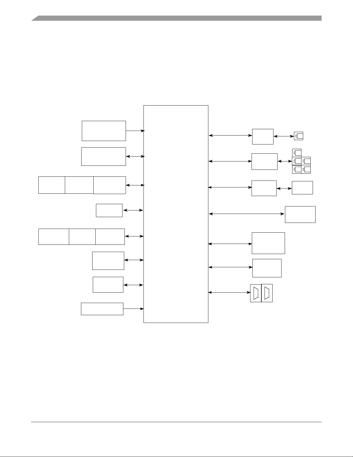
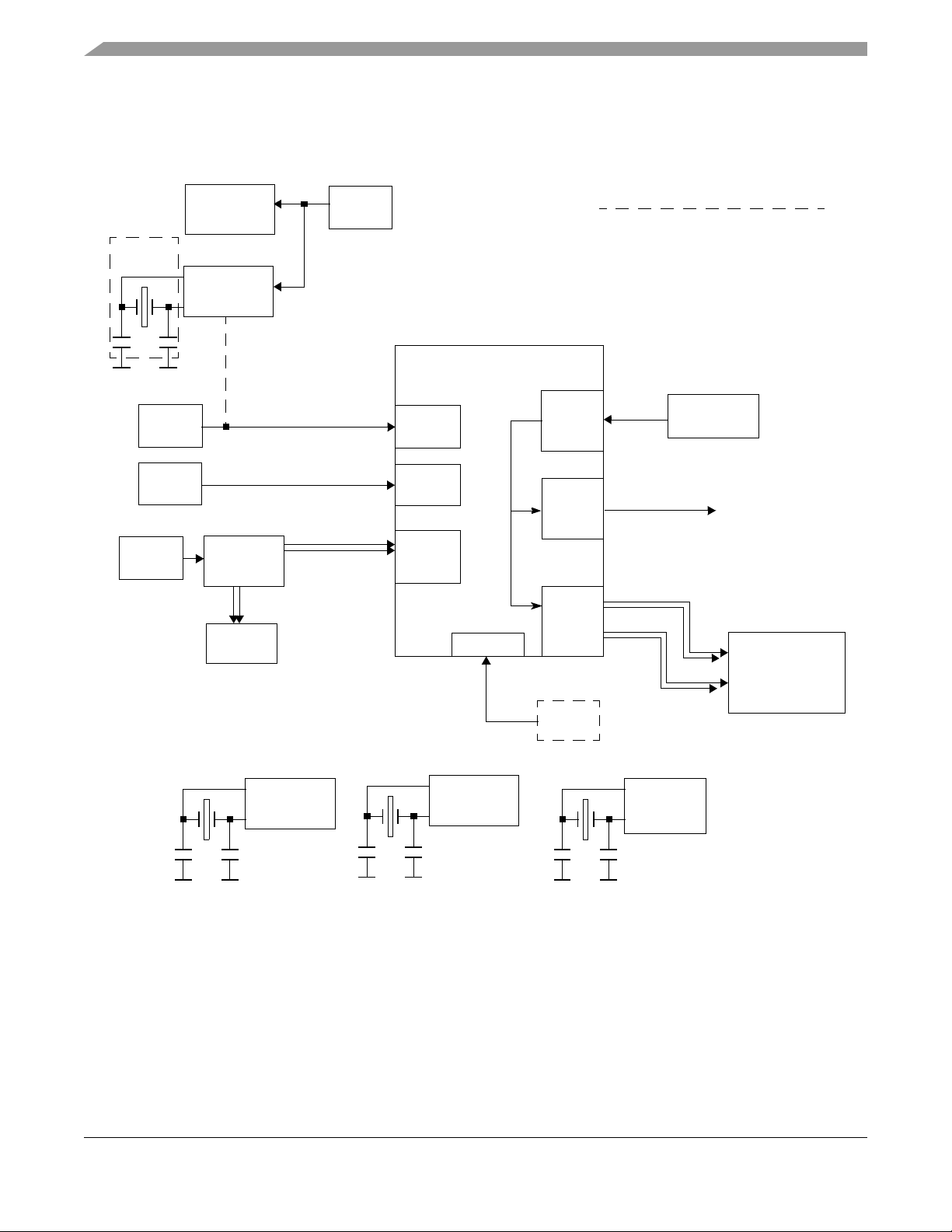
MPC8308
eTSEC2
Vitesse
L2 Switch
RGMII
ULPI
SMSC
USB PHY
IEEE1588
eTSEC1
Realtek
PHY
Clock, pulse, etc.
USB
Dual
UART
USB
mini-AB
eSDHC
SD card
System Clock
and USB Clock
128 Mbyte
DDR2
8 Mbyte
32-Bit DDR2
Bus
32 Mbyte
8/16-Bit Local
Bus
I2C Bus
Real-Time
Clock
Thermal
Sensor
GPIO
Header/
JTAG/COP
Header
JTAG/COP
Power Supply
Header/
EEPROM
RGMII
IEEE1588
Test points
Clocks
PCIe
mini PCI
Express
Connector
Test points
SPI
Header
Vitesse
L2 Switch
NAND Flash
NOR Flash
— Mini-ITX form factor (170 mm x 170 mm, or 6693 mils x 6693 mils)
• 6-layer PCB (4-layer signals, 2-layer power and ground) routing
• Certification
— CE (Class A) / FCC (Class A)
• Lead-Free (RoHS)
Figure 1 shows the MPC8308_RDB block diagram.
Figure 1. MPC8308_RDB Block Diagram
4 Micetek International Inc.
PowerQUICC™ MPC8308_RDB User’s Guide, Rev. 3
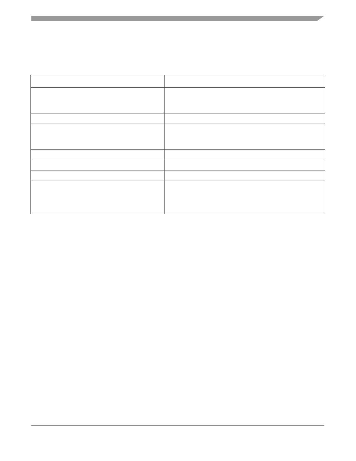
1.2 Specifications
Table 1 lists the specifications of the MPC8308_RDB.
Table 1. MPC8308_RDB Specifications
Characteristics Specifications
Power requirements (without add-on card): Typical Maximum
12 V DC 0.5 A
5.0 V DC 1.5 A
Communication processor MPC8308 running @ 400 MHz
MPC8308_RDB Hardware
Addressing: Total address range
Flash memory (local bus)
DDR2 SDRAM
Operating temperature 0o C to 70o C
Storage temperature –25oC to 85oC
Relative humidity 5% to 90% (noncondensing)
PCB dimensions:
Length
Width
Thickness
4 Gbyte (32 address lines)
8 Mbyte with one chip-select
128 Mbyte DDR2 SDRAM
6693 mil
6693 mil
62 mil
PowerQUICC™ MPC8308_RDB User’s Guide, Rev. 3
Micetek International Inc. 5
MPC8308_RDB Hardware
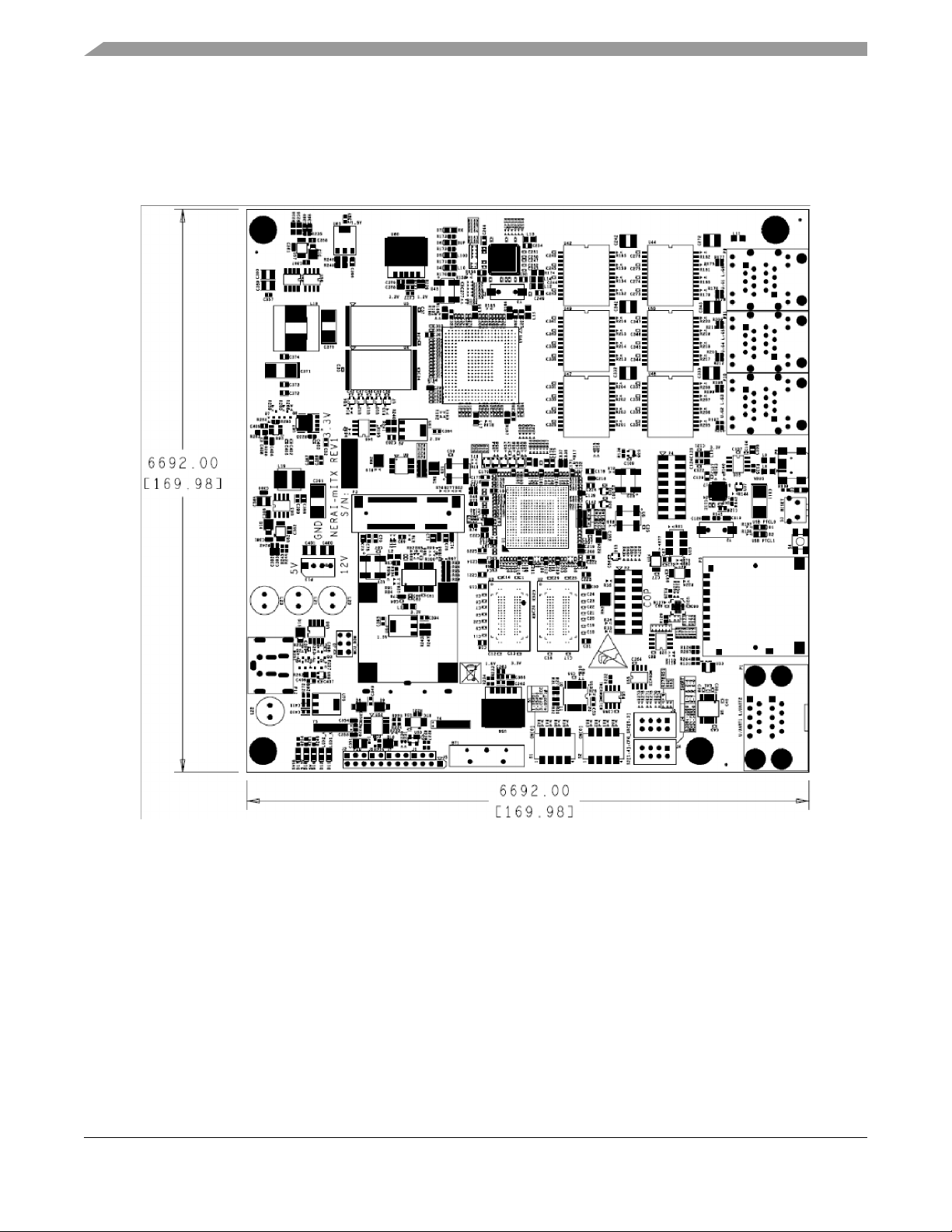
1.3 Mechanical Data
Figure 2 shows the MPC8308_RDB dimensions (in mil and [mm]). The board measures 170 mm × 170
mm (6693 mil × 6693 mil) for integration in a mini-ITX chassis.
Figure 2. Dimensions of the MPC8308_RDB
PowerQUICC™ MPC8308_RDB User’s Guide, Rev. 3
6 Micetek International Inc.

Board-Level Functions
2 Board-Level Functions
The board-level functions includes reset, external interrupts, clock distribution, DDR SDRAM controller,
local bus controller, I2C interfaces, SD memory card interface, USB interface, eTSEC1 and eTSEC2
10/100/1000 BaseT interface, dual RS-232 ports, PCI Express, and COP/JTAG.
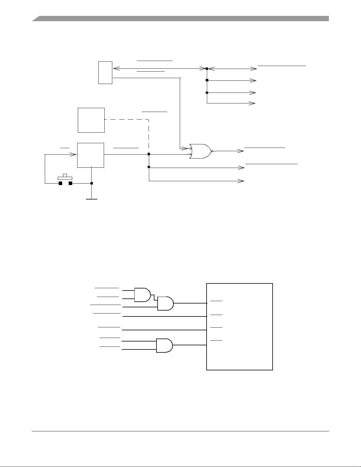
2.1 Reset and Reset Configurations
The MPC8308_RDB reset module generates a single reset to the MPC8308 and other peripherals on the
board. The reset unit provides power-on reset, hard reset, and soft reset signals in compliance with the
MPC8308 hardware specification. Figure 3 shows the reset circuitry. Notice the following:
• PORESET (Power-on reset) is generated by the Micrel MIC811 device. When MR is deasserted
and 3.3 V is ready, the MIC811 internal timeout guarantees a minimum reset active time of 150 ms
before PORESET is deasserted. This circuitry guarantees a 150 ms PORESET pulse width after
3.3 V reaches the right voltage level, and this meets the specification of the PORESET input of
MPC8308. Push button reset interfaces the MR signal with debounce capability to produce a
manual master PORESET
• PORESET (Power-on reset) is optionally generated by the MC9S08 MCU device by monitoring
the 3.3V voltage level
• HRESET (Hard reset) is generated either by the MPC8308 or the COP/JTAG port.
• COP/JTAG port reset provides convenient hard-reset capability for a COP/JTAG controller. The
HRESET line is available at the COP/JTAG port connector. The COP/JTAG controller can directly
generate the hard-reset signal by asserting this line low. The arrangement shown in Figure 3 allows
the COP to independently assert HRESET or TRST, while ensuring that the MPC8308 can drive
HRESET as well.
PowerQUICC™ MPC8308_RDB User’s Guide, Rev. 3
Micetek International Inc. 7
Board-Level Functions
MIC811
MR
Push Button
GND
COP_HRESET
COP_TRST
PORESET
NAND FLASH
mini-PCIe
MPC8308_HRESET
Vitesse VSC7385
MC9S08
Optional MCU PORESET
RTL8211B PHYs
COP
MPC8308_TRST
MPC8308_PORESET
MPC8308
TSEC1_IRQ
(RTC_IRQ)
USB_IRQ
L2_IRQ0
L2_IRQ1
THERM_IRQ
IRQ1
IRQ3
IRQ4
(MCU_IRQ)
IRQ0
Figure 3. Reset Circuitry of the MPC8308
2.2 External Interrupts
Figure 4 shows the external interrupt circuitry to the MPC8308.
Following are descriptions of the interrupt signals shown in Figure 4:
8 Micetek International Inc.
PowerQUICC™ MPC8308_RDB User’s Guide, Rev. 3
Figure 4. MPC8308 Interrupt Circuitry

Board-Level Functions
• All external interrupt signals are pulled up by 4.7 K resistors.
• MCU interrupt (MCU_IRQ), RTC interrupt (RTC_IRQ) and Thermal interrupt (THERM_IRQ).
The MCU and DS1339 RTC interrupts are ANDed the thermal interrupt. However, MCU interrupt
is the main function for this IRQ pin. RTC and thermal interrupt are optional so they are
disconnected from the AND gate by default.
• PHY interrupt (TSEC1_IRQ). The RTL8211B GBE PHY interrupt is connected to IRQ1 of the
MPC8308. Therefore, the system software can detect the status of the Ethernet link and the PHY
internal status.
• USB over current (USB_IRQ). The USB power supply have an over current detection circuit and
generate an interrupt when the current limit reaches (2A) or a thermal shutdown or under voltage
lockout (UVLO) condition occurs. It is connected to IRQ3 of the MPC8308.
• L2 Switch (VSC7385) interrupt (L2_IRQ1, L2_IRQ0). The L2 Switch (VSC7385) has two IRQs
that are ANDed together to generate an interrupt to the MPC8308E via the IRQ4 signal.
PowerQUICC™ MPC8308_RDB User’s Guide, Rev. 3
Micetek International Inc. 9
Board-Level Functions
MPC8308
DDR2 SDRAM
CLK
LCLKx
MCK1
MCK2
133 MHz
local bus
DLL
DDR
DLL
33.333 MHz
OSC
CLKIN
System
PLL
125MHz
OSC
TSEC2_GTX_CLK125
PCIE
CLK GEN
25MHz
OSC
SD_REF_CLK
SD_REF_CLK#
mini PCIe
Slot
PCIe/
Serdes
eTSEC2
ULPI USB
GND GND
24 MHz
Crystal
PHY
RTL8211B
GBE PHY
GND GND
25 MHz
Crystal
VSC7385
50MHz
VCXO
IEEE1588
DS1339
RTC
GND
32.768 kHz
Crystal
MC9S08
MCU
GND GND
32.768 kHz
Crystal
GND
Not use
125MHz
OSC
TSEC1_GTX_CLK125
eTSEC1
dotted line is optional which might not
be available
L2 Switch
25MHz
OSC
2.3 Clock Distribution
Figure 5 and Table 2 show the clock distribution on the MPC8308_RDB.
Figure 5. MPC8308_RDB Clock Scheme
10 Micetek International Inc.
PowerQUICC™ MPC8308_RDB User’s Guide, Rev. 3
Board-Level Functions
Table 2. Clock Distribution
Clock Frequency Module Generated by Description
33.333 MHz MPC8308 CLKIN 33.333 MHz oscillator The MPC8308 uses CLKIN to generate the
internal system PLL. The CSB clock is
generated by the internal PLL and is fed to the
e300 core PLL for generating the e300 core
clock.
133 MHz DDR2 SDRAM MPC8308 The DDR memory controller is configured to use
the 2:1 mode CSB to DDR for the DDR interface
(DDR266). The local bus clock uses 1:1 local to
CSB clock, which is configured by hard reset
configuration or SPMR register.
25 MHz L2 Switch and GBE PHY 25 MHz oscillator The 25 MHz oscillator provides the clock for the
L2 switch and the GBE PHY
125 MHz eTSEC1 clock 125 MHz oscillator
(default)
or RTL8211B (optional)
125 MHz eTSEC2 clock 125 MHz oscillator The eTSEC2 reference clock is provided by a
100 MHz PCIe/SERDES PCIe Clock Generator The PCIe Clock Generator provides differential
50 MHz IEEE1588 Clock (TMR_CLK) 50 MHz oscillator/ 50
MHz VCXO
24 MHz ULPI external USB PHY 24 MHz crystal Clock for ULPI USB PHY USB3300
32.768kHz MCU MC9S08 32.768kHz Crystal Clock for MCU
32.768kHz RTC DS1339 32.768kHz Crystal Clock for RTC
The eTSEC1 reference clock is provided by
a125MHz oscillator or optionally by the gigabit
Ethernet PHY (RTL8211B) on the board.
125MHz oscillator.
clock for PCIe/SERDES module and the PCIe &
mini PCIe slots
50 MHz is used by the IEEE 1588 module. It can
be an ordinary oscillator or VCXO controlled by
SPI DAC.
2.4 DDR2 SDRAM Controller
The MPC8308 processor uses DDR2 SDRAM as the system memory. The DDR2 interface uses the SSTL2
driver/receiver and 1.8 V power. A Vref 1.8 V /2 is needed for all SSTL2 receivers in the DDR2 interface.
For details on DDR2 timing design and termination, refer to the Freescale application note entitled
Hardware and Layout Design Considerations for DDR Memory Interfaces (AN2582). Signal integrity test
results show this design does not require terminating resistors (series resistor (RS) and termination resistor
(RT)) for the discrete DDR2 devices used. DDR2 supports on-die termination; the DDR2 chips and
MPC8308 are connected directly. The interface is 1.8 V provided by an on-board voltage regulator. VREF,
which is half the interface voltage, that is, 0.9 V, is provided by a voltage divider of the 1.8 V for voltage
tracking and low cost. One pair of clock pins is provided by the MPC8308, and they are connected and
shared by the two DDR2 devices. Figure 6 shows the DDR2 SDRAM controller connection.
PowerQUICC™ MPC8308_RDB User’s Guide, Rev. 3
Micetek International Inc. 11
 Loading...