

Page 1

7I43/7I43H MANUAL
V3.0
Page 2

This page intentionally not blank
Page 3

iii
Table of Contents
GENERAL . . . . . . . . . . . . . . . . . . . . . . . . . . . . . . . . . . . . . . . . . . . . . . . . . . . . . . . . . . 1
DESCRIPTION . . . . . . . . . . . . . . . . . . . . . . . . . . . . . . . . . . . . . . . . . . . . . . . . . 1
HARDWARE CONFIGURATION . . . . . . . . . . . . . . . . . . . . . . . . . . . . . . . . . . . . . . . . 2
GENERAL . . . . . . . . . . . . . . . . . . . . . . . . . . . . . . . . . . . . . . . . . . . . . . . . . . . . 2
FPGA CONFIGURATION SOURCE . . . . . . . . . . . . . . . . . . . . . . . . . . . . . . . . . 2
USB POWER . . . . . . . . . . . . . . . . . . . . . . . . . . . . . . . . . . . . . . . . . . . . . . . . . . 2
POWER ENABLE . . . . . . . . . . . . . . . . . . . . . . . . . . . . . . . . . . . . . . . . . . . . . . . 2
CONNECTOR POWER . . . . . . . . . . . . . . . . . . . . . . . . . . . . . . . . . . . . . . . . . . 3
BUS SWITCH MODE . . . . . . . . . . . . . . . . . . . . . . . . . . . . . . . . . . . . . . . . . . . . 3
PRE-CONFIGURATION PULL-UPS . . . . . . . . . . . . . . . . . . . . . . . . . . . . . . . . . 3
CONNECTORS . . . . . . . . . . . . . . . . . . . . . . . . . . . . . . . . . . . . . . . . . . . . . . . . . . . . . . 4
CONNECTOR LOCATIONS AND DEFAULT JUMPER POSITIONS . . . . . . . . 4
I/O CONNECTORS . . . . . . . . . . . . . . . . . . . . . . . . . . . . . . . . . . . . . . . . . . . . . 6
JTAG CONNECTOR . . . . . . . . . . . . . . . . . . . . . . . . . . . . . . . . . . . . . . . . . . . . 8
POWER CONNECTOR . . . . . . . . . . . . . . . . . . . . . . . . . . . . . . . . . . . . . . . . . . 8
EPP INTERFACE CONNECTOR . . . . . . . . . . . . . . . . . . . . . . . . . . . . . . . . . . . 9
OPERATION . . . . . . . . . . . . . . . . . . . . . . . . . . . . . . . . . . . . . . . . . . . . . . . . . . . . . . . 10
FPGA . . . . . . . . . . . . . . . . . . . . . . . . . . . . . . . . . . . . . . . . . . . . . . . . . . . . . . . 10
EPP CONFIGURATION . . . . . . . . . . . . . . . . . . . . . . . . . . . . . . . . . . . . . . . . . 10
USB CONFIGURATION . . . . . . . . . . . . . . . . . . . . . . . . . . . . . . . . . . . . . . . . . 11
EEPROM CONFIGURATION . . . . . . . . . . . . . . . . . . . . . . . . . . . . . . . . . . . . . 12
EXTRA EEPROM SPACE . . . . . . . . . . . . . . . . . . . . . . . . . . . . . . . . . . . . . . . 12
RECONFIGURATION . . . . . . . . . . . . . . . . . . . . . . . . . . . . . . . . . . . . . . . . . . . 13
CONFIGURATION FILE STARTUP OPTIONS . . . . . . . . . . . . . . . . . . . . . . . . 13
SC7I43P and SC7I43W . . . . . . . . . . . . . . . . . . . . . . . . . . . . . . . . . . . . . . . . . 13
CLOCK SIGNALS . . . . . . . . . . . . . . . . . . . . . . . . . . . . . . . . . . . . . . . . . . . . . . 14
EPP-FPGA INTERFACE . . . . . . . . . . . . . . . . . . . . . . . . . . . . . . . . . . . . . . . . 14
USB-FPGA INTERFACE . . . . . . . . . . . . . . . . . . . . . . . . . . . . . . . . . . . . . . . . 15
ADDITIONAL 7I43H INTERFACE PINS . . . . . . . . . . . . . . . . . . . . . . . . . . . . . 16
LEDS . . . . . . . . . . . . . . . . . . . . . . . . . . . . . . . . . . . . . . . . . . . . . . . . . . . . . . . 16
BUS SWITCH MODE . . . . . . . . . . . . . . . . . . . . . . . . . . . . . . . . . . . . . . . . . . . 17
I/O LEVELS . . . . . . . . . . . . . . . . . . . . . . . . . . . . . . . . . . . . . . . . . . . . . . . . . . 17
STARTUP I/O STATE . . . . . . . . . . . . . . . . . . . . . . . . . . . . . . . . . . . . . . . . . . 18
DRIVING 5V REFERRED LOADS . . . . . . . . . . . . . . . . . . . . . . . . . . . . . . . . . 18
TERMINATION . . . . . . . . . . . . . . . . . . . . . . . . . . . . . . . . . . . . . . . . . . . . . . . . 18
Page 4

iv
Table of Contents
SUPPLIED CONFIGURATIONS . . . . . . . . . . . . . . . . . . . . . . . . . . . . . . . . . . . . . . . 19
EPPIOPR8 . . . . . . . . . . . . . . . . . . . . . . . . . . . . . . . . . . . . . . . . . . . . . . . . . . . 19
USBIOPR8 . . . . . . . . . . . . . . . . . . . . . . . . . . . . . . . . . . . . . . . . . . . . . . . . . . . 20
LBP . . . . . . . . . . . . . . . . . . . . . . . . . . . . . . . . . . . . . . . . . . . . . . . . . . . 21
EXAMPLE COMMANDS . . . . . . . . . . . . . . . . . . . . . . . . . . . . . . . . . . . 22
LOCAL LBP COMMANDS . . . . . . . . . . . . . . . . . . . . . . . . . . . . . . . . . . 23
LOCAL LBP READ COMMANDS . . . . . . . . . . . . . . . . . . . . . . . . . . . . . 23
LOCAL LBP WRITE COMMANDS . . . . . . . . . . . . . . . . . . . . . . . . . . . . 25
RPC COMMANDS . . . . . . . . . . . . . . . . . . . . . . . . . . . . . . . . . . . . . . . . 26
EXAMPLE RPC COMMAND LIST . . . . . . . . . . . . . . . . . . . . . . . . . . . . 27
AVAILABLE DAUGHTER CARDS . . . . . . . . . . . . . . . . . . . . . . . . . . . . . . . . . . . . . . 28
REFERENCE INFORMATION . . . . . . . . . . . . . . . . . . . . . . . . . . . . . . . . . . . . . . . 29
SPECIFICATIONS . . . . . . . . . . . . . . . . . . . . . . . . . . . . . . . . . . . . . . . . . . . . . 29
Page 5

7I43 1
GENERAL
DESCRIPTION
The 7I43 is a USB/EPP version of the FPGA based Anything I/O card series. It
provides 48 programmable I/O bits The 7I43H variant is a high speed USB version.
Initial FPGA configurations can be downloaded to the 7I43 via the USB (7I43 and
7I43H) or EPP (7I43 only) port. The 7I43/7I43H also has a serial EEPROM for FPGA
configuration storage when the 7I43/7I43H is used in stand-alone applications.
The 48 I/O bits are available on two 50 pin connectors, 24 bits per connector. The
50 pin connectors have I/O module rack compatible pin-outs. The connector pin-out uses
interleaved grounds for lower crosstalk and controlled impedance.
/Done, /Init and power status LEDs are provided for debugging puposes as are 8
FPGA driven LEDs. Several I/O interface daughter cards are available for the 7I43/7I43H.
These cards include a 4 axis 3A Hbridge, a 2 Axis 3A stepper motor driver, an analog
servo amp. interface, an RS-422/485 interface, and a debug LED card. One daughter card
can plug directly onto the 7I43/7I43H.
Many IO configuration files are provided with the 7I43/7I43H including simple
remote I/O, 4 and 8 axis servo motion control, 4 and 8 axis microstepping stepper motor
control, multiple channel PWM generator, quadrature counters and more. VHDL source
is provided for all configurations.
FPGA system clock is 50MHZ Oscillator. The Spartan3 used can multiply or divide
this frequency to suitable values for application use.
The 7I43 uses a 200K or 400K gate Xilinx SpartanIII FPGA, and the 7I43H uses
a 400K SpartanIII FPGA. Free development tools for the SpartanIII are available (Xilinx
WebPack) from Xilinx’s web site.
Page 6

7I43 2
HARDWARE CONFIGURATION
GENERAL
Hardware setup jumper positions assume that the 7I43 or 7I43H card is oriented in
an upright position, that is, with the USB connector towards the person doing the
configuration, and the power connector on top right. In the following, "7I43" refers to both
the 7I43 and the 7I43H.
FPGA CONFIGURATION SOURCE
The 7I43's FPGA can be configured via the USB port, The EPP port, or the on card
serial EEPROM. Jumpers W4 and W5 select the configuration source. The 7I43H does
not have the EPP configuration option.
W4 W5 MODE
DOWN DOWN EPP (PARALLEL PORT) CONFIG
DOWN UP USB CONFIG
UP DOWN EEPROM CONFIG
USB POWER
The 7I43 can be powered by the USB host. The maximum power that can be
supplied by a USB host is 450 mA. This will be sufficient for most but not all 7I43
applications. For applications that require more than the 450 mA supplied by the host, the
7I43 has provisions for external power. W6 connects host USB power to the 7I43's power
supplies. To use host power, W6 must be set to the "UP" position. If external 5Vpower is
used, W6 must be set to the "DOWN" position.
WARNING: Connecting an external 5V supply to the 7I43 while W6 is in the "UP"
position and a USB cable connects the 7I43 to a host computer is likely to damage
the computer by feeding external power ‘backwards’ into the USB port!
POWER ENABLE
The 7I43 can be set to power-up only after the USB interface is activated. This is
the suggested operational mode when the 7I43 is interfaced via USB. For applications
where the 7I43 must operate without the USB interface, This function must be disabled.
W7 controls the power up enable mode. When W7 is in the "UP" position, the 7I43 power
supplies are always enabled. When W7 is in the "DOWN" position, the 7I43 power
supplies will only be enabled when the USB interface is active.
Page 7

7I43 3
HARDWARE CONFIGURATION
CONNECTOR POWER
The power connection on both I/O connectors (Pin 49) can supply either 3.3V or
5V power. Supplied power should be limited to 400 mA total. W1 selects the power
supplied to both P3 and P4 . When W1 is in the "UP" position, 5V power is supplied to the
connector. When W1 is in the "DOWN" position, 3.3V power is supplied to P3 and P4.
Note that most Mesa I/O adapter cards that connect to Anything I/O cards require 5V.
BUS SWITCH MODE
Jumper W2 determines bus switch mode for all user I/O pins. When jumper W2 is
in the "UP" position, 5V tolerant mode is selected, when ‘down’, 3.3V mode is selected.
Note that 3.3V mode is not 5V tolerant. The FPGA can be damaged by input voltages
greater than 4V in 3.3V mode.
PRE-CONFIGURATION PULL-UPS
The 7I43 has no pull-up resistors on its user I/O pins. This means that before these
pins are configured, they will not have a defined state. If this is not desired, internal pull-up
resistors on all FPGA pins can be enabled via Jumper W3. When W3 is in the "DOWN"
position, user I/O will float until the FPGA is configured. When W3 is in the "UP" position,
all FPGA pins including user I/O pins will have a pull-up resistor to 3.3V so the pins will be
in a "HIGH" state. It is suggested that the internal pull-ups be enabled unless this causes
a problem with connected I/O devices. Note that once the FPGA is configured, each FPGA
input pin can have programmable pull-up or pull-down resistors.
Page 8
7I43 4
CONNECTORS
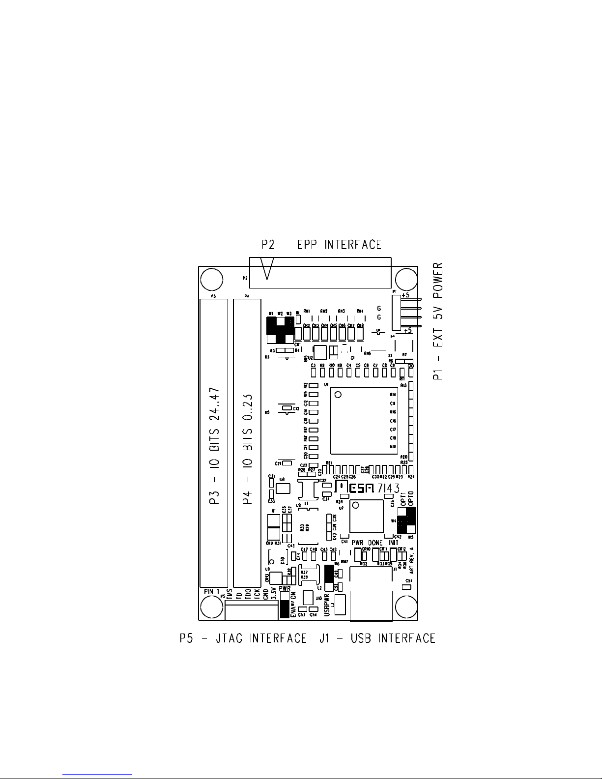
CONNECTOR LOCATIONS AND DEFAULT JUMPER POSITIONS
7I43-U shown -P version has different defaults
Page 9
7I43 5
CONNECTORS
7I43H CONNECTOR LOCATIONS AND DEFAULT JUMPER POSITIONS
Page 10

7I43 6
CONNECTORS
I/O CONNECTORS
P3 and P4 are the 7I43s I/O connectors. These are 50 pin box headers that mate
with standard 50 conductor female IDC connectors. For information on which I/O pin
connects to which FPGA pin, please see the 7I43IO.PIN file on the 7I43 distribution disk.
7I43 IO connector pinouts are as follows:
P4 CONNECTOR PINOUT
PIN FUNC PIN FUNC PIN FUNC PIN FUNC
1 IO0 2 GND 3 IO1 4 GND
5 IO2 6 GND 7 IO3 8 GND
9 IO4 10 GND 11 IO5 12 GND
13 IO6 14 GND 15 IO7 16 GND
17 IO8 18 GND 19 IO9 20 GND
21 IO10 22 GND 23 IO11 24 GND
25 IO12 26 GND 27 IO13 28 GND
29 IO14 30 GND 31 IO15 32 GND
33 IO16 34 GND 35 IO17 36 GND
37 IO18 38 GND 39 IO19 40 GND
41 IO20 42 GND 43 IO21 44 GND
45 IO22 46 GND 47 IO23 48 GND
49 POWER 50 GND
Page 11

7I43 7
CONNECTORS
7I43 I/O CONNECTORS
P3 CONNECTOR PINOUT
PIN FUNC PIN FUNC PIN FUNC PIN FUNC
1 IO24 2 GND 3 IO25 4 GND
5 IO26 6 GND 7 IO27 8 GND
9 IO28 10 GND 11 IO29 12 GND
13 IO30 14 GND 15 IO31 16 GND
17 IO32 18 GND 19 IO33 20 GND
21 IO34 22 GND 23 IO35 24 GND
25 IO36 26 GND 27 IO37 28 GND
29 IO38 30 GND 31 IO39 32 GND
33 IO40 34 GND 35 IO41 36 GND
37 IO42 38 GND 39 IO43 40 GND
41 IO44 42 GND 43 IO45 44 GND
45 IO46 46 GND 47 IO47 48 GND
49 POWER 50 GND
Page 12

7I43 8
CONNECTORS
7I43 JTAG CONNECTOR
P5 is a JTAG programming connector. It is not normally used since the 7I43 can be
programmed via the USB or EPP interface, but can be useful when debugging or
reprogramming the CPLD. 3.3V levels are used for JTAG signals. A single JTAG
connector is used for both the CPLD and the FPGA, with the CPLD being first in the JTAG
chain.
P6 CONNECTOR PINOUT
PIN FUNCTION DIRECTION
1 TMS IN
2 TDI IN
3 TDO OUT
4 TCK IN
5 GND
6 +3.3V
POWER CONNECTOR
The 7I43 has an external 5V power connector, P1. This connector supplies power
to the 7I43 in EPP, standalone, and USB applications where USB host power is not
sufficient to power the 7I43. On 7I43 card with revisions B or less, P1 is a four pin .1"
male header. On 7I43s with revision C or greater or 7I43Hs’, P1 is a 2 pin 3.5MM
pluggable screw terminal block. P1 pin-out is as follows:
P1 PINOUT (REV B and <) P1 PINOUT (7I43 Rev C and >, all 7I43H)
PIN FUNCTION PIN FUNCTION
1 +5V 1 +5V
2 GND 2 GND
3 GND
4 +5V
Page 13

7I43 9
CONNECTORS
EPP INTERFACE CONNECTOR
On the 7I43 (but not the 7I43H), P2 is the EPP printer port interface connector. P2
is a 26 pin header. P2 pin-out matches stands DB25 printer port pin-out, allowing a simple
flat cable with a DB25M IDC connector on one end and a 26 pin female header on the
other end to interface the hosts printer port to the 7I43.
P2 PIN DB25 PIN SIGNAL P2 PIN DB25 PIN SIGNAL
1 1 /STROBE 2 14 /AUTOFD
3 2 PD0 4 15 /FAULT
5 3 PD1 6 16 /INIT
7 4 PD2 8 17 /SELECTIN
9 5 PD3 10 18 GND
11 6 PD4 12 19 GND
13 7 PD5 14 20 GND
15 8 PD6 16 21 GND
17 9 PD7 18 22 GND
19 10 /ACK 20 23 GND
21 11 BUSY 22 24 GND
23 12 PERROR 24 25 GND
25 13 SELECT 26 VCC
Note: All handshake signals are available at the CPLD but only /STROBE,
/AUTOFD,/SELECTIN and BUSY are forwarded to the FPGA with the standard CPLD
configuration.
Page 14

7I43 10
OPERATION
FPGA
The 7I43/7I43H uses a Xilinx Spartan-III FPGA in a 144 pin QFP package, Either
PN XC3S200-5PQ144C or XC3S400-5PQ144C depending on 7I43 model.
HOST INTERFACE
The 7I43 uses either a USB or EPP printer port interface to the host. The 7I43H is
USB only. These interfaces can be used for programming the FPGA and accessing the
FPGA once programmed.
EPP CONFIGURATION
When the7I43 is jumpered so the configuration source is EPP, and the FPGA is not
configured (DONE is low), the on card CPLD implements two EPP registers to allow
configuring the FPGA via the EPP port.
The two EPP registers are the control register and the data register. The control
register is at EPP address 1 and has a single output bit (at D0) that controls FPGA
/PROGRAM, and a single input bit (at D0) that reads the FPGA’s done status. The data
register at EPP address 0, is used for the byte wide configuration data. Reads from the
data register will return the FPGA size in D0, 1 = 400K and 0 = 200K.
EPP CONFIGURATION PROCEDURE
EPPWriteAddress(1) ; Select EPP address 0x01 = control register
EPPWriteData(0) ; Set /PROGRAM low
EPPWriteData(1) ; Set /PROGRAM High
(Wait 100 Usec) ; Wait 100 Usec for FPGA to initialize
EPPWriteAddress(0) ; Select EPP address 0x00 = data register
EPPReadData ; Verify FPGA size
EPPWriteData(FPGAByte0) ; Write first byte of FPGA config data
EPPWriteData(FPGAByte1) ; Write second byte of FPGA config data
(write remaining FPGA config bytes)
Page 15

7I43 11
OPERATION
EPP CONFIGURATION
Once the FPGA is configured, the CPLD EPP registers and EPP handshake logic
are disabled and it is the FPGA’s responsibility to handle the EPP host interface. The
CPLD is still used at this point to forward some of the EPP port handshaking lines through
to the FPGA for 5V tolerance.
USB CONFIGURATION
When the7I43 is jumpered so the configuration source is USB, and the FPGA is not
configured (DONE is low), the on card CPLD implements a simple data handshake so all
data sent to the USB port is written to the FPGAs configuration port.
The CPLD also will echo characters to indicate the FPGA size and DONE status.
If a character is sent to the 7I43 and the characters LSb is ‘1' the DONE status will be
returned in the echoed characters LSb. If a character with a ‘0' LSb is sent, a character will
be echoed indicating the FPGA size. This echoed character will have a ‘0' LSb for 200K
7I43s and a ‘1' LSb for 400K 7I43s. Since it in not desirable to deal with echoed
characters for every configuration byte sent to the 7I43, status character echoing is
disabled after receiving 4 consecutive characters with a ‘0' LSB..
Once the FPGA is configured the CPLD data handshake is disabled and it is the
FPGA’s responsibility to handle the interface to the USB chip.
USB CONFIGURATION PROCEDURE
Flush receive buffer ; Optional
Send "1" character ; Optional
Check echoed character for LSb = 0 (done should be low ; Optional
Send "0" character ; Optional
Check echoed character LSb to determine FPGA size ; Optional
Send 4 more "0" characters ; Disable echo
Send configuration byte 0
Send configuration byte 1
(Send remaining configuration bytes)
Page 16

7I43 12
OPERATION
EEPROM CONFIGURATION
For stand-alone applications and when it is not desired to have to preconfigure the
FPGA via the host interface at power up, the 7I43 can be configured via its serial
EEPROM. Of course the Serial EEPROM must first be programmed with the desired
configuration file. The serial EEPROM used is a ST M25P20 SPI flash serial EEPROM.
All access the serial EEPROM is via the FPGA, so programming the serial
EEPROM is a "bootstrap" process, where the first step is programming the FPGA with a
configuration giving host (EPP or USB) access to the serial EEPROM through the FPGA.
Both the EPP and USB GPIO demo configurations allow this EEPROM access via a
simple SPI interface built into the configuration.
The SCM7I43P program is an example program for writing the serial EEPROM via
the EPP port (DOS only), SCM7I43W is a similar example program for writing the serial
EEPROM via the USB port (windows only) The SCM programs rely on EPPIOPR8 (for
EPP programming or USBIOPR8 (for USB) configuration file being preloaded into the
FPGA before writing the serial EEPROM, as the serial EEPROM can only be accessed
through the FPGA. EPPIOPR8 and USBIOPR8 have a simple SPI interface to allow
EEPROM access.
EXTRA EEPROM SPACE
The serial configuration EEPROM on the 7I43 has a capacity of 256K bytes, but the
configuration bit file for the 400K Spartan 3 chip is only ~208K bytes, leaving 48 K bytes
free for FPGA accessible non volatile storage. The 200K gate Spartan 3 chip uses only
~128K bytes of the serial EEPROM leaving 128K bytes free. This storage can be used for
non-volatile settings or program storage in stand-alone 7I43 applications.
Page 17

7I43 13
OPERATION
RECONFIGURATION
Once the 7I43 is configured, the CPLD loader is disabled. In order to reconfigure
the FPGA, the FPGA must be reset via /PROGRAM. This can be done by having the
FPGA assert its /RECONFIG pin (drive it low). If you wish to have the ability to reconfigure
the FPGA without cycling the power, the FPGA configuration must include some way of
asserting /RECONFIG. /RECONFIG is FPGA pin 52 on the 7I43 and pin 44 on the 7I43H.
Note that pin 52 is also USB2CLK input on the 7I43H. This means that you should
not load a standard 7I43/7I43H to a configuration file to a 7I43H and configure the USB
chip for synchronous operation, not only will it not work, it will cause a bus conflict.
CONFIGURATION FILE STARTUP OPTIONS
Important: Because the 7I43s CPLD stops configuration when DONE is asserted,
the configuration file startup options must be set so that asserting DONE is the last
configuration step. Suggested startup options are as follows:
FPGA STARTUP CLOCK: CCLK
DONE: 6
ENABLE OUTPUTS: 5
RELEASE WRITE ENABLE: 4
RELEASE DLL: NO WAIT
SC7I43P and SC7I43W
Two utility programs, SC7I43P.EXE and SC7I43W are provided to send
configuration files to the 7I43. SC7I43P is a DOS only program and SC7I43W is a windows
only program.
SC7I43P is invoked with the FPGA configuration file and the Hexadecimal EPP port base
address on the command line:
SC7I43P FPGAFILE.BIT 378
SC7I43W is invoked with the FPGA configuration file and the COM port on the command
line:
SC7I43W FPGAFILE.BIT COM6
SC7I43P and SC7I43W use binary FPGA configuration files. These files can
standard Xilinx BIT files or Xilinx PROM format files.
Page 18

7I43 14
OPERATION
CLOCK SIGNALS
The 7I43 has a 50 MHz crystal controlled clock signal routed to pin 53 (GCLK3) on
the FPGA. Four user I/O pins are also GCLK pins:
IO BIT GCLK FPGA PIN IO BIT GCLK FPGA PIN
IOBIT0 GCLK6 127 IOBIT24 GCLK7 128
IOBIT17 GCLK4 124 IOBIT40 GCLK5 125
EPP-FPGA INTERFACE
The interface from host EPP printer port to the FPGA uses 12 FPGA pins. These
consist of an eight bit bidirectional data bus (D0..D7), and four handshake lines. Note that
the handshake lines are fed through the CPLD so depend on the standard CPLD
configuration. The D bus connects to the FPGA through 100 Ohm resistors. These
resistors provide 5V tolerance and series line termination for driving the cable.
P2 PIN EPPNAME SPPNAME FPGA PIN DIRECTION
1 /WRITE /STROBE 84 TO FPGA
2 /DSTROBE /AUTOFD 79 TO FPGA
8 /ASTROBE /SELECTIN 80 TO FPGA
21 WAIT BUSY 82 FROM FPGA
3 D0 D0 68 BIDIR
5 D1 D1 63 BIDIR
7 D2 D2 60 BIDIR
9 D3 D3 59 BIDIR
11 D4 D4 51 BIDIR
13 D5 D5 50 BIDIR
15 D6 D6 47 BIDIR
17 D7 D7 46 BIDIR
Page 19

7I43 15
OPERATION
EPP-FPGA INTERFACE
The EPP interface implements a simple multiplexed 8 bit data/address bus. The
EPPIOPR8 configuration can be used as an example of an EPP interface in the FPGA.
This is a simple GPIO interface organized as six eight bit ports.
USB-FPGA INTERFACE
The USB interface differs between the 7I43 and 7I43H. The 7I43 uses a FTDI USB
interface chip, the FT245R. This is a Full speed interface chip (12 Mbps max). The
FT245R appears as a single endpoint communication device, basically a simple
bidirectional byte-stream with receive and transmit FIFOs. In order to use the USB
configuration and interface you must load the appropriate drivers for you operating system.
These drivers are available at FTDICHIP.COM. The utilities supplied with the 7I43 utilize
the VCP (Virtual COM Port) series drivers.
The 7I43H uses a FT2232H high speed USB interface chip (480 Mbps). Unlike the
FT245R used in the 7I43, the FT2232H appears as two serial ports. Only the first port is
used by the 7I43H. The supplied configurations support the same FIFO interface mode as
the 7I43 and the same pinout, but the 7I43H also has the FPGA connections to support
the high speed synchronous mode that allows host transfer rates up to 25M bytes per
second. The default mode is limited to 10 M bytes per second.
The FPGA interface uses a bidirectional 8 bit data bus that is shared with the EPP
interface on the 7I43). Because of this sharing you cannot operate the USB and EPP
interfaces simultaneously.
SIGNAL NAME FPGA PIN DIRECTION FUNCTION
USBWRITE 56 FROM FPGA XMIT DATA STROBE
/USBRD 55 FROM FPGA RECV DATA STROBE
/USBTXE 83 TO FPGA XMIT FIFO NOT FULL
/USBRXF 69 TO FPGA RECV FIFO HAS DATA
D0 68 BIDIR DATA BUS
D1 63 BIDIR DATA BUS
D2 60 BIDIR DATA BUS
D3 59 BIDIR DATA BUS
Page 20

7I43 16
OPERATION
SIGNAL NAME FPGA PIN DIRECTION FUNCTION
D4 51 BIDIR DATA BUS
D5 50 BIDIR DATA BUS
D6 47 BIDIR DATA BUS
D7 46 BIDIR DATA BUS
ADDITIONAL 7I43H USB INTERFACE PINS
The 7I43H can use the FT2232H’s high speed synchronous FIFO interface mode
and the SPI mode on channel B. These additional pins are connected as follows:
SIGNAL NAME FPGA PIN DIRECTION FUNCTION
USB2CLK 52 TO FPGA SYNC FIFO CLOCK
/USB2OE 82 FROM FPGA SYNC FIFO OUTPUT
ENABLE
UDI 57 FROM FPGA SPI DATA IN
UDO 84 TO FPGA SPI DATA OUT
USK 85 TO FPGA SPI CLOCK
/UCS 79 TO FPGA SPI CHIP SELECT
LEDS
The 7I43 has 8 FPGA driven user LEDS. These green LEDS are located in the top
center of the card. They can be used for any purpose, and can be helpful as a simple
debugging feature. A low output signal from the FPGA lights the LED. See the
7I43MISC.PIN file for FPGA pin locations of the LED signals.
In addition to the user LEDs there are three other LEDS that display board status
information. These status LEDS are on the lower right hand side of the card just above the
USB connector, The LEDS are a yellow PWR LED, a red /DONE LED and a red /INIT
LED. The /DONE and /INIT LED can be used to determine FPGA configuration status. The
/INIT LED will be illuminated when /PROGRAM is asserted or when a CRC error has
occurred during the configuration process. The /DONE LED will be illuminated when the
FPGA is not configured.
Page 21

7I43 17
OPERATION
BUS SWITCH MODE
The 7I43 uses bus switch devices in series with all I/O pins. These devices allow
the 7I43 inputs to be 5V tolerant and allow the I/O pins to be pulled up to 5V. The bus
switch input protection function works by disconnecting the FPGA from the IO pins when
the IO pin voltage rises above a preset threshold. This threshold determines the bus switch
operational mode. We refer to the modes as 5V tolerant mode and 3.3V mode.
When in 5V tolerant mode, the inputs and tri-stated outputs may be pulled up to 5V.
This allows driving 5V referred loads such as I/O module racks and connecting inputs to
5V logic. The disadvantage of 5V mode is that the output impedance is higher in the high
output state (when the FPGA pins are at 3.3V) as the bus switch is off when the FPGA pin
is at 3.3V.
When 3.3V mode is selected, the bus switch is always fully on unless input voltages
>4V are applied, at which point the bus switch disconnects the FPGA from the I/O pin.
3.3V mode is suggested for general use. Note that 3.3V mode is not 5V tolerant. When
the bus switch mode jumper W2 is in the ‘up’ position, 5V mode is selected, when ‘down’,
3.3V bus switch mode is selected.
IO LEVELS
The FPGA used on the 7I43 is a Spartan3. The Spartan3 supports many I/O
standards. The 7I43 does not support use of the I/O standards that require input reference
voltages, also VCCIO is fixed at 3.3V. The available I/O options for are LVTTL,
LVCMOS_33, LVDCI_33, and LVDCI_33_DV2 .
The Spartan3 FPGA chip used on the 7I43 is not 5V tolerant but external bus switch
parts are used on the 7I43 to make the I/O pins 5V tolerant. The bus switch parts
disconnect the FPGA pins from the I/O pins when the I/O pins are driven to positive
voltage levels that would damage the FPGA.
The voltage level that causes disconnect can be selected to be ~4V (3.3V mode)
or ~3.3V (5Vmode). For most applications, the 3.3V mode should be used. The 5V tolerant
mode is useful when driving 5V referred loads or accepting 5V logic levels.
Note that there is no protection against negative input voltages other than the input
clamp diodes in the FPGA and bus switches, so negative input voltages must be limited
to -.5V
Page 22

7I43 18
OPERATION
STARTUP I/O STATE
When the 7I43 is used to control external equipment that is sensitive to the initial
pin states, the pre-configuration pull-ups should be enabled (W3 UP), and for most
configurations, pull-ups resistor should be configured on any I/O pin that is not driven when
configuration is complete (bi-directional pins and pins whose function is assigned by
software). Since the only definable pre-configuration state is with pull-up resistors on the
I/O, this means the proper I/O polarity is active low (so that all outputs are in the in-active
state at power up)
DRIVING +5V REFERRED LOADS
When driving external loads like Solid State Relays (SSRs) with an active low
output, and the +SSR terminal connected to +5V, the 7I43 output should be configured for
5V tolerance, and the output should be driven in open drain mode. This is because the
7I43 outputs only swing to 3.3V in normal mode, leaving 1.7V (5V -3.3V) driving the SSR
when the output is high and the SSR should be off.
TERMINATION
The FPGA used on the 7I43 supports series and parallel termination that can be
programmed on a pin-for-pin basis. This feature is called DCI. The 7I43 supports DCI on
all user I/O pins. The DCI reference resistors are all 100 Ohm 1%.
Page 23

7I43 19
SUPPLIED CONFIGURATIONS
EPPIOPR8
GENERAL
The EPPIOPR8 configuration is a simple six port GPIO configuration with EPP
interface. The GPIO is organized as six eight bit ports, each with an associated Data
Direction Register (DDR).The EPPIOPR8 configuration can be used as a starting point for
more complicated user configurations. There are two EPPIOPR8 configuration files,
EPPIO8-2.BIT for the 200K and EPPIO8-4.BIT for 400K versions of the 7I43.
PORT DATA REG DDR IO BITS CONNECTOR
0 0x10 0x20 0..7 P4
1 0x11 0x21 8..15 P4
2 0x12 0x22 16..23 P4
3 0x13 0x23 24..31 P3
4 0x14 0x24 32..39 P3
5 0x15 0x25 40..47 P3
In addition to the GPIO bits, the EPPIOPR8 configuration has a simple SPI interface
to the configuration EEPROM and a reconfiguration port.. The SPI port allows the utility
program SCM7I43P to write configuration data to the serial EEPROM. These registers are
mapped as follows:
REGISTER ADDRESS FUNCTION
SPICS 0x7D Single I/O bit to control SPI Chip Select (bit 0)
SPIDATA 0x7E Eight bit SPI shift register
RECONFIG 0x7F Reconfig - Writing 0x5A here resets FPGA
The 7I43 is delivered with the EPPIOPR8 configuration installed for factory and
initial user checking.
Page 24

7I43 20
SUPPLIED CONFIGURATIONS
USBIOPR8
GENERAL
The USBIOPR8 configuration is a simple six port GPIO configuration almost
identical to the EPPIOPR configuration. It is different because the USB interface is a
simple bidirectional byte-stream without separate address and data. Because of this a
Little Binary Protocol (LBP) is used to communicate with standard addressable peripherals
in the 7I43 FPGA configuration. The GPIO is organized as six eight bit ports, each with an
associated Data Direction Register (DDR).The USBIOPR8 configuration can be used as
a starting point for more complicated user configurations. There are two USBIOPR8
configuration files, USBIO8-2.BIT for the 200K and USBIO8-4.BIT for 400K versions of the
7I43.
PORT DATA REG DDR IO BITS CONNECTOR
0 0x010 0x020 0..7 P4
1 0x011 0x021 8..15 P4
2 0x012 0x022 16..23 P4
3 0x013 0x023 24..31 P3
4 0x014 0x024 32..39 P3
5 0x015 0x025 40..47 P3
In addition to the GPIO bits, the USBIOPR8 configuration has a simple SPI interface
to the configuration EEPROM, a LED port, and a reconfiguration port.. The SPI port allows
the utility program SCM7I43W to write configuration data to the serial EEPROM. These
registers are mapped as follows:
REGISTER ADDRESS FUNCTION
LED 0x07A 8 Status LEDS (‘1' = on)
SPICS 0x07D Single I/O bit to control SPI Chip Select (bit 0)
SPIDATA 0x07E Eight bit SPI shift register
RECONFIG 0x07F Reconfig - Writing 0x5A here resets FPGA
Page 25

7I43 21
SUPPLIED CONFIGURATIONS
USBIOPR8
LBP
LBP is a simple master slave protocol where the host sends read, write, or RPC
commands to the 7I43, and the 7I43 responds. LBP allows the host (master) to efficiently
access registers on the slave (7I43) via a simple bidirectional byte oriented protocol.
LBP commands always start with a command header byte. This header specifies
whether the command is a read or a write, the number of address bytes(0, or 2), and the
number of data bytes(1 through 8).The 0 address size option indicates that the current
address pointer should be used. This address pointer will be post incremented by the data
size if the auto increment bit is set.
RPC commands allow any of up to 64 stored commands to be executed in response
to the single byte command.
LBP DATA READ/WRITE COMMAND
0 1 WR RID AI AS DS1 DS0
Bit 7.. 6 CommandType: Must be 01b to specify data read/write command
Bit 5 Write: 1 to specify write, 0 to specify read
Bit 4 RPCIncludesData: 0 specifies that data is from stream, 1, that data is from
RPC (RPC only, ignored for non RPC commands)
Bit 3 AutoInc: 0 leaves address unchanged, 1 specifies that address is post
incremented by data size in bytes.
BIT 2 AddressSize: 0 to specify current address, 1 to specify 2 byte address.
Bit 1..0 DataSize: Specifies data size, 00b = 1 bytes, 01b = 2 bytes, 10 b= 4 bytes,
011b = 8 bytes.
When multiple bytes are specified in a read or write command, the bytes are always
written to or read from successive addresses. That is, a 4 byte read at location 0x21 will
read locations 0x21, 0x22, 0x23, 0x24. The address pointer is not modified after the
command unless the AutoInc bit is set.
Page 26

7I43 22
SUPPLIED CONFIGURATIONS
USBIOPR8
EXAMPLE LBP COMMANDS
Write 4 bytes (0xAA, 0xBB,0xCC,0xDD) to addresses 0x010,0x011,0x012,0x013
with AutoInc so that the address pointer will be left at 0x014 when the command is
completed:
COMMAND BITS CT1 CT0 WR RID AI AS DS1 DS0
LBPWrite: 2 add 4 data
0 1 1 0 1 1 1 0
Write Address LSB 0 0 0 1 0 0 0 0
Write Address MSB 0 0 0 0 0 0 0 0
Write data 0 1 0 1 0 1 0 1 0
Write Data 1 1 0 1 1 1 0 1 1
Write Data 2 1 1 0 0 1 1 0 0
Write Data 3 1 1 0 1 1 1 0 1
Write 2 more bytes (0xEE,0xFF) at 0x014 and 0x015:
COMMAND BITS CT1 CT0 WR RID AI AS DS1 DS0
LBPWrite: 0 add 2 data
0 1 1 0 0 0 0 1
Write data 0 1 1 1 0 1 1 1 0
Write data 1 1 1 1 1 1 1 1 1
Read 8 bytes at 0x010,0x011,0x012,0x013,0x014,0x015,0x016,0x017:
COMMAND BITS CT1 CT0 WR RID AI AS DS1 DS0
LBPRead: 2 add 8 data
0 1 0 0 0 1 1 1
Read Address LSB 0 0 0 1 0 0 0 0
Read Address MSB 0 0 0 0 0 0 0 0
Page 27

7I43 23
SUPPLIED CONFIGURATIONS
USBIOPR8
LOCAL LBP COMMANDS
In addition to the basic data access commands there are a set of commands that
access LBP status and control the operation of LBP itself. These are organized as READ
and WRITE commands
LOCAL LBP READ COMMANDS
(HEX), all of these commands return a single byte of data.
0xC0 Get unit address (dont-care for USB devices)
0xC1 Get LBP status
LBP Status bit definitions:
BIT 7 Reserved
BIT 6 Command Timeout Error
BIT 5 Invalid write Error (attempted write to protected area)
BIT 4 Buffer overflow error
BIT 3 Watchdog timeout error
BIT 2 Reserved
BIT 1 Reserved
BIT 0 CRC error
0xC2 Get CRC enable status
0xC3 Get CRC error count
0xC4 .. 0xC9 Reserved
0xCA Get Enable_RPCMEM access flag
0xCB Get Command timeout (in mS for USB and character times/10 for serial)
0xCC Get Non-volatile memory flag
0xCD Get External memory flag
0xCE.. 0xCF Reserved
Page 28

7I43 24
SUPPLIED CONFIGURATIONS
USBIOPR8
LOCAL LBP READ COMMANDS
0xD0 .. 0xD3 4 character card name
0xD5 .. 0xD7 4 character configuration name (only on some configurations)
0xD8 Get low address
0xD9 Get high address
0xDA Get LBP version
0xDB Get LBP Unit ID (Serial only, not used with USB)
0xDC Get RPC Pitch
0xDD Get RPC SizeL (Low byte of RPCSize)
0xDE Get RPC SizeH (High byte of RPCSize)
0xDF Get LBP cookie (returns 0x5A)
Page 29

7I43 25
SUPPLIED CONFIGURATIONS
USBIOPR8
LOCAL LBP WRITE COMMANDS
(HEX), all of these commands except 0xFF expect a single byte of data.
0xE0 Reserved
0xE1 Set LBP status (0 to clear errors)
0xE2 Set CRC check enable (Flag non-zero to enable CRC checking)
0xE3 Set CRC error count
0xE4 .. 0xE9 Reserved
0xEA Set Enable_RPCMEM access flag (non zero to enable access to RPC memory)
0xEB Set Command timeout (in mS for USB and character times for serial)
0xEC Set Non-volatile memory flag
0xED Set External memory flag (non zero for external memory mode)
0xEE .. 0xEF Reserved
0xF0 .. 0xF6 Reserved
0xF7 Write LEDs
0xF8 Set low address
0xF9 Set high address
0xFA Add byte to current address
0xFB .. 0xFC Reserved
0xFD Set unit ID (serial only)
0xFE Reset LBP processor if followed by 0x5A
0xFF Reset LBP parser (no data follows this command)
Page 30

7I43 26
SUPPLIED CONFIGURATIONS
USBIOPR8
RPC COMMANDS
RPC commands allow previously stored sequences of read/write commands to be
executed with a single byte command. Up to 64 RPC’s may be stored. RPC write
commands may include data if desired, or the data may come from the USB serial data
stream. RPCs allow significant command compression which improves communication
bandwidth.
LBP RPC COMMAND
1 0 RPC5 RPC4 RPC3 RPC2 RPC1 RPC0
Bit 7..6 CommandType: must be 10b to specify RPC
Bit 5..0 RPCNumber: Specifies RPC 0 through 63
In the USBIOPR8 configuration, RPCPitch is 0x10 bytes so each RPC command
has native size of 0x10 bytes and start 0x10 byte boundaries in the RPC table area. RPCs
can cross RPCPitch boundaries if larger than RPCPitch RPCs are needed. The stored
RPC commands consist of LBP headers and addresses, and possibly data if the command
header has the RID bit set. RPC command lists are terminated by a 0 byte.
The RPC table is accessed at addresses 0 through RPCSize-1 This means with a
RPCPitch of 0x10 bytes, RPC0 starts at 0x0000, RPC1 starts at 0x0010, RPC2 starts at
0x0020 and so on.
Before RPC commands can be written to the RPC table, the RPCMEM access flag
must be set. The RPCMEM access flag must be clear for normal operation.
Page 31

7I43 27
SUPPLIED CONFIGURATIONS
USBIOPR8
EXAMPLE RPC COMMAND LIST
This is an example stored RPC command list. Note RPC command lists must start
at a RPCPitch boundary in the RPC table but an individual RPC list can extend until the
end of the table. This particular RPC example contains 3 LBP commands and uses 11
bytes starting at 0x0050 (RPC5 for 0x10 pitch RPC table)
Command1. Writes two data bytes to port 0x10, 0x11 with 2 data bytes supplied by host
Command2. Reads two data bytes from port 0x12,0x13
Command3. Writes a single byte (0xAA) to port 0x14, data contained in RPC table
COMMAND BITS CT1 CT0 WR RID I AS DS1 DS0
LBPWrite: 2 add 2 data
0 1 1 0 0 1 0 1
Write Address LSB 0 0 0 1 0 0 0 0
Write Address MSB 0 0 0 0 0 0 0 0
LBPRead: 2 add 2 data
0 1 0 0 0 1 0 1
Read Address LSB 0 0 0 1 0 0 1 0
Read Address MSB 0 0 0 0 0 0 0 0
LBPWrite 2 add 1 data
1 0 1 1 0 1 0 0
Write Address LSB 0 0 0 1 0 1 0 0
Write Address MSB 0 0 0 0 0 0 0 0
Write Data 1 0 1 0 1 0 1 0
Terminator
0 0 0 0 0 0 0 0
The data stream for this RPC would consist of these 3 bytes:
COMMAND BITS CT1 CT0 R5 R4 R3 R2 R1 R0
RPC 5
1 0 0 0 0 1 0 1
Data 0 for Command 1 0 1 0 1 0 1 0 1
Data 1 for Command 1 1 1 0 0 1 1 0 0
Page 32

7I43 28
AVAILABLE DAUGHTER CARDS
PART NUMBER FUNCTION
7I29 Dual 20A 165V HBridge
7I30 Quad 3A 36V HBridge
7I31 Debug LED card
7I32 Dual stepper driver (microstepping)
7I33,7I33T Quad analog servo interface
7I34 8 TX + 8 RX pair RS-422 interface
7I34-R 16 RX pair RS-422 interface
7I37,7I37T 8 output 16 input isolated I/O
7I39 Dual 3 phase H-Bridge
7I40 Dual H-Bridge
7I42 I/O protector
7I44 8 Channel RS-422 to RJ45 breakout
7I46 6 channel SPI breakout
7I47 12 channel encoder oriented RS-422 interface
7I47S 12 channel encoder interface with isolated spindle analog out
7I48 6 channel analog servo interface
7I49 6 channel resolver interface
7I50 SPI I/O expander
7I64 24 input, 24 output isolated I/O
7I65 Octal16 bit A-D analog servo interface
7I66-8 16 input 8 output isolated I/O
7I66-24 24 output isolated I/O
Page 33

7I43 29
REFERENCE INFORMATION
SPECIFICATIONS
MIN MAX NOTES
SUPPLY VOLTAGE 4.5V 5.25V
3.3V CURRENT TO P2,P3,P4,P5 ---- 800mA T y p i c a l l y
limited to
~200 mA in
USB powered
case.
5V CURRENTTO P3,P4 ---- 2A Typically limited to
~150 mA in USB
powered case.
1.2V CORE POWER CURRENT ---- 1A 1A = ~300 mA of 5V
draw. Depends on
FPGA configuration
MAXIMUM I/O I SINK OR I SOURCE ---- 24mA
MAXIMUM I/O INPUT VOLTAGE -.5V 5.5V 5V Tolerant mode.
I/O 0..47, EPP I/O
MAXIMUM I/O INPUT VOLTAGE -.5V 4V 3.3V mode. I/O 0..47
TEMPERATURE -C VERSION 0oC 70oC
TEMPERATURE -I VERSION -40oC 85oC
 Loading...