

Page 1

7I37/7I37T/7I37TA MANUAL
Isolated Anything-IO adapter
V2.1
Page 2

This page intentionally almost blank
Page 3

iii
Table of Contents
GENERAL . . . . . . . . . . . . . . . . . . . . . . . . . . . . . . . . . . . . . . . . . . . . . . . . . . . . . . . . . . 1
DESCRIPTION . . . . . . . . . . . . . . . . . . . . . . . . . . . . . . . . . . . . . . . . . . . . . . . . . 1
OPTION JUMPERS . . . . . . . . . . . . . . . . . . . . . . . . . . . . . . . . . . . . . . . . 1
CONNECTORS . . . . . . . . . . . . . . . . . . . . . . . . . . . . . . . . . . . . . . . . . . . . . . . . . . . . . . 2
CONNECTOR LOCATIONS . . . . . . . . . . . . . . . . . . . . . . . . . . . . . . . . . . . . . . . 2
CONTROLLER CONNECTOR . . . . . . . . . . . . . . . . . . . . . . . . . . . . . . . . . . . . . 4
50 PIN ISOLATED I/O CONNECTOR . . . . . . . . . . . . . . . . . . . . . . . . . . . . . . . 5
TERMINAL BLOCK ISOLATED I/O CONNECTOR . . . . . . . . . . . . . . . . . . . . . 7
OPERATION . . . . . . . . . . . . . . . . . . . . . . . . . . . . . . . . . . . . . . . . . . . . . . . . . . . . . . . . 9
CONTROLLER REQUIREMENTS . . . . . . . . . . . . . . . . . . . . . . . . . . . . . . . . . . 9
PINOUT . . . . . . . . . . . . . . . . . . . . . . . . . . . . . . . . . . . . . . . . . . . . . . . . . 9
POLARITY . . . . . . . . . . . . . . . . . . . . . . . . . . . . . . . . . . . . . . . . . . . . . . . 9
I/O VOLTAGES . . . . . . . . . . . . . . . . . . . . . . . . . . . . . . . . . . . . . . . . . . . 9
INPUT CHARACTERISTICS . . . . . . . . . . . . . . . . . . . . . . . . . . . . . . . . . . . . . . 9
OUTPUT CHARACTERISTICS . . . . . . . . . . . . . . . . . . . . . . . . . . . . . . . . . . . . 9
OUTPUT TRANSISTORS . . . . . . . . . . . . . . . . . . . . . . . . . . . . . . . . . . . 9
INDUCTIVE LOADS . . . . . . . . . . . . . . . . . . . . . . . . . . . . . . . . . . . . . . . . 9
AC LOADS . . . . . . . . . . . . . . . . . . . . . . . . . . . . . . . . . . . . . . . . . . . . . . 10
SPECIFICATIONS . . . . . . . . . . . . . . . . . . . . . . . . . . . . . . . . . . . . . . . . . . . . . . . . . . 11
DRAWINGS . . . . . . . . . . . . . . . . . . . . . . . . . . . . . . . . . . . . . . . . . . . . . . . . . . . . . . . 12
Page 4

7I37 1
GENERAL
DESCRIPTION
This manual applies to the 7I37, 7I37T and 7I37TA. They will referred to as 7I37
unless a distinction is required. The 7I37 is an 8 output, 16 input isolated I/O interface
card. The 7I37 provides 8 Isolated 48VDC 1A output drivers and 16 Opto-isolated inputs.
All output drivers are low saturation voltage MOSFETS for low power dissipation. Each of
the 8 output switches is isolated from the others, allowing high side, low side, push-pull
and other output switch configurations. The 16 opto-isolated inputs will operate with input
voltages from 4 to 24 V. Reverse protection diodes are provided to allow use with AC
inputs. The 7I37 is compatible with the all Mesa 50 pin parallel I/O and FPGA cards.
OPTION JUMPERS
The 7I37 has a single option jumper: W1. W1 determines if the 7I37 card gets its
power from pin 49 of the controller connector. When W1 is in the up position (default),
the 7I37 cards gets its power from pin 49. When W1 is in the down position, The 7I37 is
disconnected from pin 49 and must be supplied with 5V power on P1.
Page 5
7I37 2
CONNECTORS
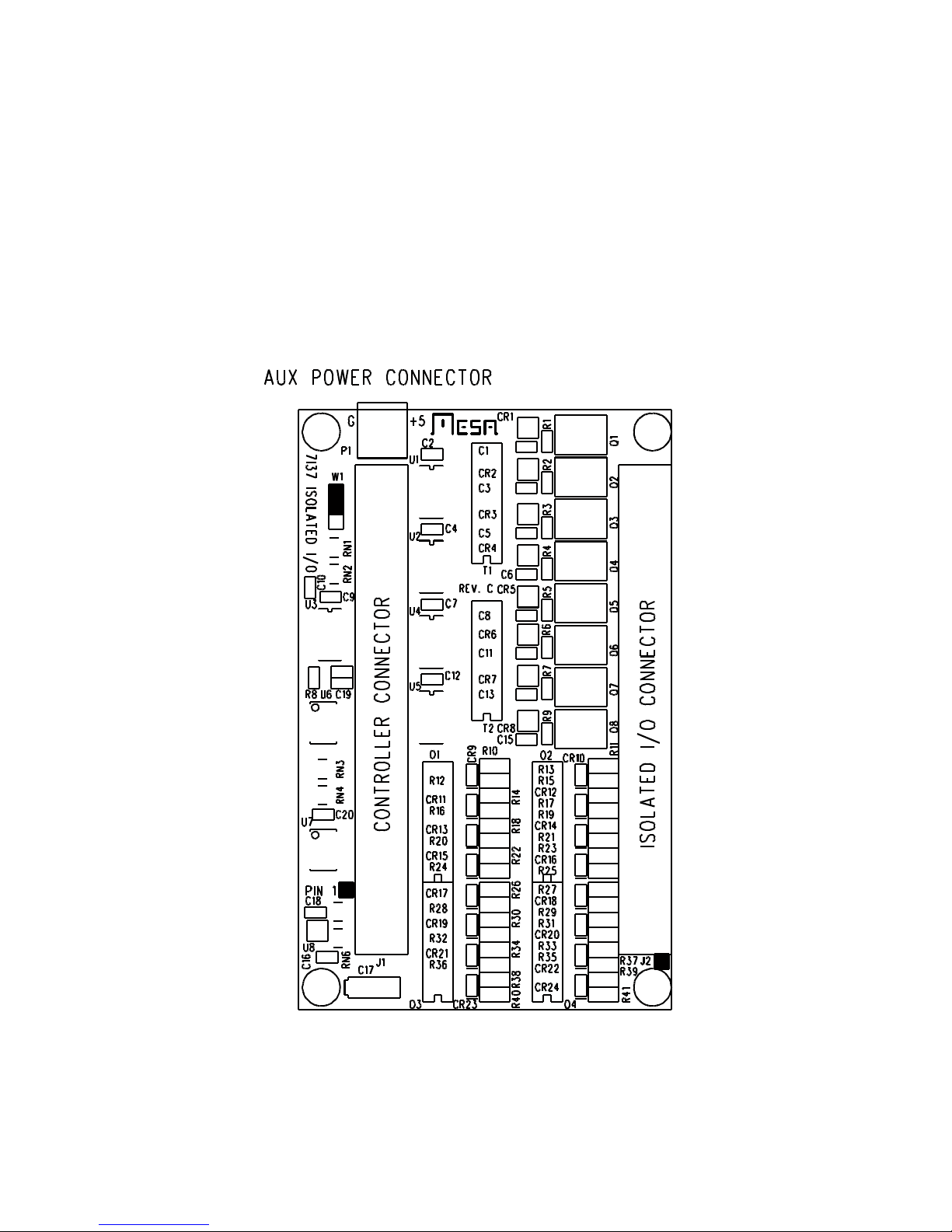
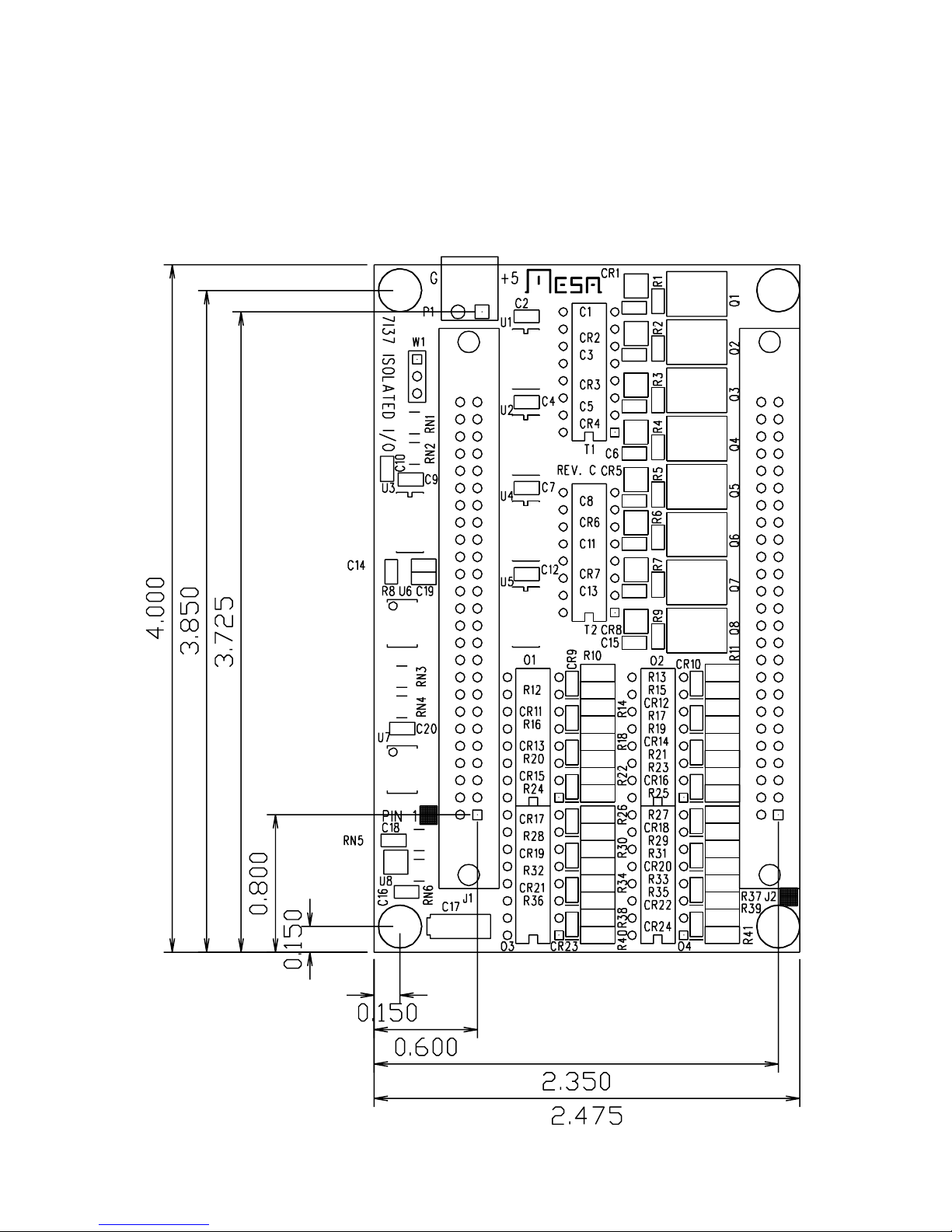
7I37 CONNECTOR LOCATIONS
Page 6
7I37 3
CONNECTORS
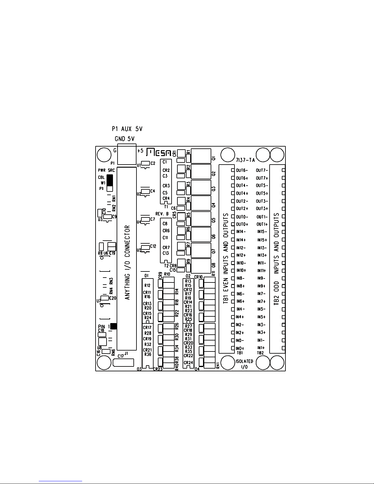
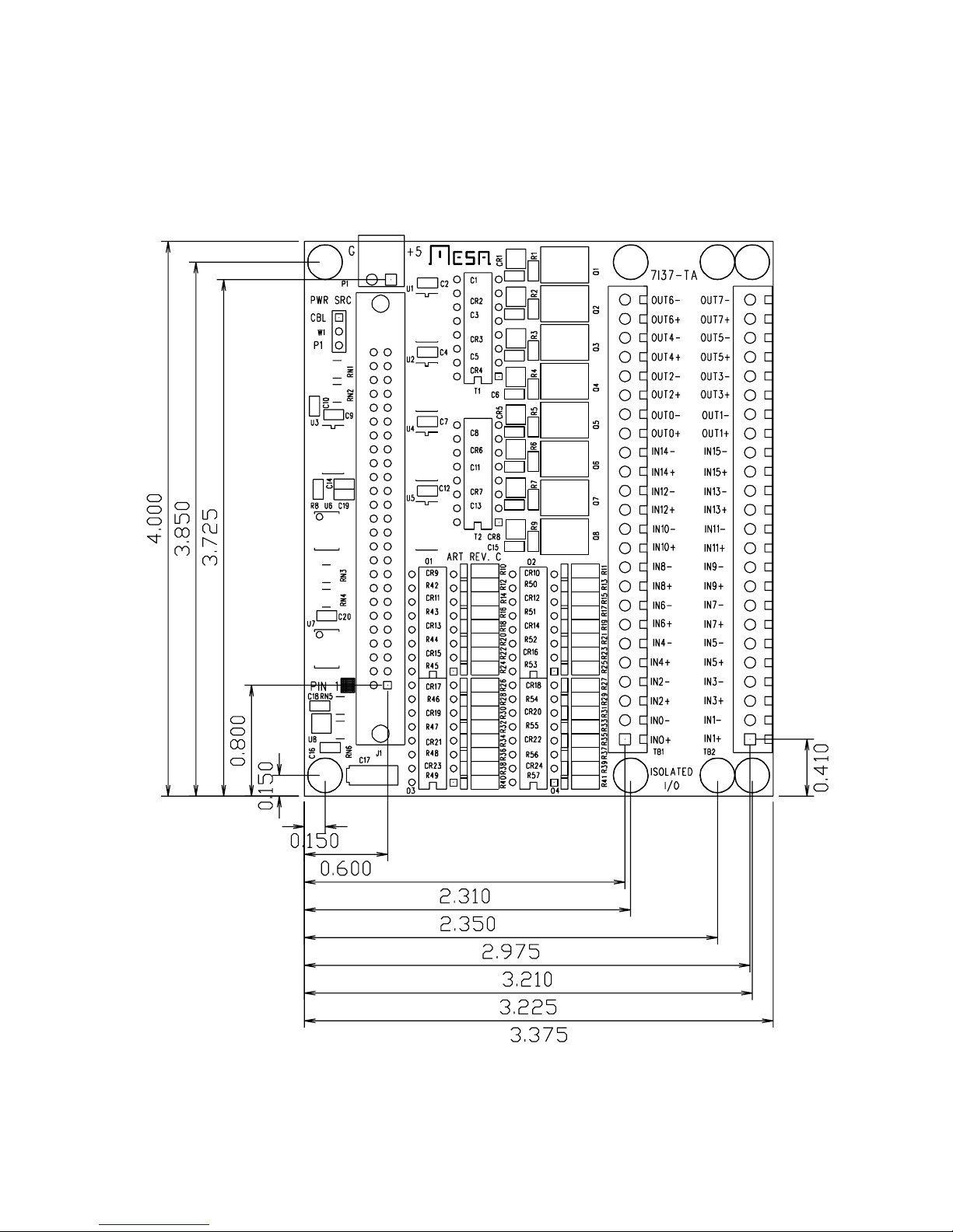
7I37TA CONNECTOR LOCATIONS
Page 7

7I37 4
CONNECTORS
CONTROLLER CONNECTOR
50 pin header connector J1 connects to the IO card that controls the 7I37 isolated
I/O card. This can be a male 50 pin header on the top of the 7I37 card or a female 50
conductor header on the bottom side of the 7I37 depending on 7I37 model:
PIN FUNCTION DIRECTION PIN FUNCTION DIRECTION
1 IN0 FROM 7I37 25 IN12 FROM 7I37
3 IN1 FROM 7I37 27 IN13 FROM 7I37
5 IN2 FROM 7I37 29 IN14 FROM 7I37
7 IN3 FROM 7I37 31 IN15 FROM 7I37
9 IN4 FROM 7I37 33 OUT0 TO 7I37
11 IN5 FROM 7I37 35 OUT1 TO 7I37
13 IN6 FROM 7I37 37 OUT2 TO 7I37
15 IN7 FROM 7I37 39 OUT3 TO 7I37
17 IN8 FROM 7I37 41 OUT4 TO 7I37
19 IN9 FROM 7I37 43 OUT5 TO 7I37
21 IN10 FROM 7I37 45 OUT6 TO 7I37
23 IN11 FROM 7I37 47 OUT7 TO 7I37
Note: all even pins are grounded. 49 +5V PWR TO 7I37
AUX 5V POWER
4 pin header P1 or 2 pin terminal block P1 can be used to supply 5V power to the
7I37 if the controller cable is too long and voltage drop too high. P1 has the following
pinout:
PIN FUNCTION PIN FUNCTION
1 5V 1 5V (Square pad)
2 GND 2 GND
3 GND
4 5V
Four pin header is used on 7I37T, 7I37TA rev. D and earlier and 7I37 rev. B and
earlier. Two pin terminal block is used on 7I37TA rev. E and later and 7I37 rev. C and later.
Page 8

7I37 5
CONNECTORS
50 PIN ISOLATED I/O CONNECTOR
The 7I37 uses 50 pin header J2 for isolated I/O header J2 pinout is as follows:
PIN FUNCTION DIRECTION PIN FUNCTION DIRECTION
1 IBIT0+ TO 7I37 2 IBIT0- TO 7I37
3 IBIT1+ TO 7I37 4 IBIT1- TO 7I37
5 IBIT2+ TO 7I37 6 IBIT2- TO 7I37
7 IBIT3+ TO 7I37 8 IBIT3- TO 7I37
9 IBIT4+ TO 7I37 10 IBIT4- TO 7I37
11 IBIT5+ TO 7I37 12 IBIT5- TO 7I37
13 IBIT6+ TO 7I37 14 IBIT6- TO 7I37
15 IBIT7+ TO 7I37 16 IBIT7- TO 7I37
17 IBIT8+ TO 7I37 18 IBIT8- TO 7I37
19 IBIT9+ TO 7I37 20 IBIT9- TO 7I37
21 IBIT10+ TO 7I37 22 IBIT10- TO 7I37
23 IBIT11+ TO 7I37 24 IBIT11- TO 7I37
25 IBIT12+ TO 7I37 26 IBIT12- TO 7I37
27 IBIT13+ TO 7I37 28 IBIT13- TO 7I37
29 IBIT14+ TO 7I37 30 IBIT14- TO 7I37
31 IBIT15+ TO 7I37 32 IBIT15- TO 7I37
Page 9

7I37 6
CONNECTORS
50 PIN ISOLATED I/O CONNECTOR
PIN FUNCTION DIRECTION PIN FUNCTION DIRECTION
33 OBIT0+ FROM 7I37 34 OBIT0- FROM 7I37
35 OBIT1+ FROM 7I37 36 OBIT1- FROM 7I37
37 OBIT2+ FROM 7I37 38 OBIT2- FROM 7I37
39 OBIT3+ FROM 7I37 40 OBIT3- FROM 7I37
41 OBIT4+ FROM 7I37 42 OBIT4- FROM 7I37
43 OBIT5+ FROM 7I37 44 OBIT5- FROM 7I37
45 OBIT6+ FROM 7I37 46 OBIT6- FROM 7I37
47 OBIT7+ FROM 7I37 48 OBIT7- FROM 7I37
Pins 49 and 50 of J2 are unused.
Page 10

7I37 7
CONNECTORS
TERMINAL BLOCK ISOLATED I/O CONNECTORS
The 7I37TA uses 3.5 mm pluggable screw terminal blocks TB1 and TB2 for isolated I/O.
TB1 pinout is as follows:
TB1
PIN FUNCTION DIRECTION PIN FUNCTION DIRECTION
1 IBIT0+ TO 7I37 2 IBIT0- TO 7I37
3 IBIT2+ TO 7I37 4 IBIT2- TO 7I37
5 IBIT4+ TO 7I37 6 IBIT4- TO 7I37
7 IBIT6+ TO 7I37 8 IBIT5- TO 7I37
9 IBIT8+ TO 7I37 10 IBIT8- TO 7I37
11 IBIT10+ TO 7I37 12 IBIT10- TO 7I37
13 IBIT12+ TO 7I37 14 IBIT12- TO 7I37
15 IBIT14+ TO 7I37 16 IBIT14- TO 7I37
17 OBIT0+ FROM 7I37 18 0BIT0- FROM 7I37
19 OBIT2+ FROM 7I37 20 OBIT2- FROM 7I37
21 OBIT4+ FROM 7I37 22 OBIT4- FROM 7I37
23 OBIT6+ FROM 7I37 24 OBIT6- FROM 7I37
Page 11

7I37 8
CONNECTORS
TERMINAL BLOCK ISOLATED I/O CONNECTORS
TB2
PIN FUNCTION DIRECTION PIN FUNCTION DIRECTION
1 IBIT1+ TO 7I37 2 IBIT1- TO 7I37
3 IBIT3+ TO 7I37 4 IBIT3- TO 7I37
5 IBIT5+ TO 7I37 6 IBIT5- TO 7I37
7 IBIT7+ TO 7I37 8 IBIT7- TO 7I37
9 IBIT9+ TO 7I37 10 IBIT9- TO 7I37
11 IBIT11+ TO 7I37 12 IBIT11- TO 7I37
13 IBIT13+ TO 7I37 14 IBIT13- TO 7I37
15 IBIT15+ TO 7I37 16 IBIT15- TO 7I37
17 OBIT1+ FROM 7I37 18 0BIT1- FROM 7I37
19 OBIT3+ FROM 7I37 20 OBIT3- FROM 7I37
21 OBIT5+ FROM 7I37 22 OBIT5- FROM 7I37
23 OBIT7+ FROM 7I37 24 OBIT7- FROM 7I37
TERMINAL BLOCK KEYING
The I/O terminal blocks on the 7I37TA are supplied with three 8 pin screw terminal
plugs. To prevent accidental misconnection if wired plugs are removed and replaced. It
may be desirable to key the plugs so they can only be inserted in their proper receptacle
location. The screw terminal plugs are keyed by clipping certain of the small green
polarizing tabs on the screw terminal plugs and installing blocking plugs (these are thin
orange plastic pieces) in the corresponding slot in the receptacle. A suggested keying
pattern for TB1 is keys at pins 2, 8, 12, 16, 21, 24 and for TB2 is keys at pins 1, 4, 9, 13,
17, 22.
Page 12

7I37 9
OPERATION
CONTROLLER REQUIREMENTS
PINOUT
The 7I37 is intended to operate with I/O cards that have 24 I/O bits and IO module
rack type connector pinouts (50 pin connector, all even pins grounded, +5 power on pin
49).
POLARITY
All controller interface pins are active low. This means a low controller output
indicates power applied to an opto-isolated input. A low output activates the corresponding
output MOSFET.
I/O VOLTAGES
The 7I37 accepts 3.3V or 5V signals and drives the FPGA card with 3.3V signals
so is compatible with 5V and 3.3V FPGA cards.
TIMING
MOSFET outputs turn on in ~3 uSec and off in ~7 uSec. Opto-isolated inputs turn
on on ~5 uSec and off in ~25 uSec.
INPUT CHARACTERISTICS
The opto-isolated inputs have 4.4K Ohm series resistors and reverse input
protection diodes across the opto-isolator LEDS. Input current an the maximum 24V input
is approximately 5mA. The isolated inputs will work with input voltages from 4 to 24V.
Note: The reverse input protection diodes are red LEDs. If you see a red LED
illuminated, this means you have reverse polarity DC or AC voltage applied to an
input.
OUTPUT CHARACTERISTICS
OUTPUT TRANSISTORS
The 7I37 outputs are small MOSFET power transistors with an on resistance of
approximately 0.25 Ohms, giving a saturation voltage of ~0.25V at full (1A) load. The
OBITx+ pins are the MOSFET drain connections and the OBITx- pins are the MOSFET
source connections. The MOSFETs have a built in drain-source diode.
INDUCTIVE LOADS
If the 7I37 outputs are used to switch inductive loads such as relays, some provision
for limiting the turn-off spike must be provided, such as a free wheeling diode across the
load or a R/C snubber.
Page 13

7I37 10
OPERATION
OUTPUT CHARACTERISTICS
AC LOADS
The 7I37 can drive low voltage (up to 24VAC) AC loads by series connecting two
outputs. For example a 24V AC switch could be created by connecting OBIT0+ to OBIT1+
and using OBIT0- and OBIT1- as the output leads. An output snubber circuits should be
used across inductive loads. For AC switching, both output bits should change at the same
time
Page 14

7I37 11
SPECIFICATIONS
MIN MAX UNITS
5V POWER SUPPLY 4.5V 5.5V VDC
5V POWER CONSUMPTION --- 50 mA
INPUT RANGE 4V 28V VDC
INPUT CURRENT --- 5 mA
OUTPUT VOLTAGE --- 48V VDC
OUTPUT CURRENT --- 1A A
ISOLATION VOLTAGE1 --- 500 VDC
(Between controller and any isolated I/O)
ISOLATION VOLTAGE2 --- 100 VDC
(Between any isolated input or output)
OPERATING TEMP. 0 +70
o
C
OPERATING TEMP. (-I version) -40 +85
o
C
OPERATION HUMIDITY 0 95% NON-COND
Page 15
7I37 12
DRAWINGS
Page 16
7I37 13
DRAWINGS
 Loading...