

Page 1

7I33 / 7I33TA MANUAL
Quad analog servo amp interface
V1.9
Page 2

This page intentionally almost blank
Page 3

iii
Table of Contents
GENERAL . . . . . . . . . . . . . . . . . . . . . . . . . . . . . . . . . . . . . . . . . . . . . . . . . . . . . . . . . . 1
DESCRIPTION . . . . . . . . . . . . . . . . . . . . . . . . . . . . . . . . . . . . . . . . . . . . . . . . . 1
HARDWARE CONFIGURATION . . . . . . . . . . . . . . . . . . . . . . . . . . . . . . . . . . . . . . . . 2
DEFAULT JUMPER LOCATIONS . . . . . . . . . . . . . . . . . . . . . . . . . . . . . . . . . . 2
TTL/RS-422 ENCODER SELECTION . . . . . . . . . . . . . . . . . . . . . . . . . . . . . . . 2
CONNECTORS . . . . . . . . . . . . . . . . . . . . . . . . . . . . . . . . . . . . . . . . . . . . . . . . . . . . . . 3
7I33 CONNECTOR LOCATIONS AND DEFAULT JUMPERS . . . . . . . . . . . . . 3
7I33 CONNECTOR LOCATIONS AND DEFAULT JUMPERS . . . . . . . . . . . . . 4
CONTROLLER CONNECTOR . . . . . . . . . . . . . . . . . . . . . . . . . . . . . . . . . . . . . 5
AUX 5V POWER . . . . . . . . . . . . . . . . . . . . . . . . . . . . . . . . . . . . . . . . . . . . . . . 5
50 PIN SERVO AMP/ENCODER CONNECTOR . . . . . . . . . . . . . . . . . . . . . . . 6
TERMINAL BLOCK SERVO AMP/ENCODER CONNECTORS . . . . . . . . . . . . 7
OPERATION . . . . . . . . . . . . . . . . . . . . . . . . . . . . . . . . . . . . . . . . . . . . . . . . . . . . . . . . 9
PWM RATE . . . . . . . . . . . . . . . . . . . . . . . . . . . . . . . . . . . . . . . . . . . . . . . . . . . 9
STEP RESPONSE . . . . . . . . . . . . . . . . . . . . . . . . . . . . . . . . . . . . . . . . . . . . . . 9
ENCODER INPUT CIRCUIT . . . . . . . . . . . . . . . . . . . . . . . . . . . . . . . . . . . . . . . 9
MAXIMUM COUNT RATE . . . . . . . . . . . . . . . . . . . . . . . . . . . . . . . . . . . . . . . . 9
5V POWER . . . . . . . . . . . . . . . . . . . . . . . . . . . . . . . . . . . . . . . . . . . . . . . . . . 10
ENABLE INPUT . . . . . . . . . . . . . . . . . . . . . . . . . . . . . . . . . . . . . . . . . . . . . . . 10
ENABLE OUTPUT . . . . . . . . . . . . . . . . . . . . . . . . . . . . . . . . . . . . . . . . . . . . . 10
ANALOG OUTPUT . . . . . . . . . . . . . . . . . . . . . . . . . . . . . . . . . . . . . . . . . . . . . 10
ANALOG CONNECTIONS . . . . . . . . . . . . . . . . . . . . . . . . . . . . . . . . . . . . . . . 10
SPECIFICATIONS . . . . . . . . . . . . . . . . . . . . . . . . . . . . . . . . . . . . . . . . . . . . . . . . . . 11
DRAWINGS . . . . . . . . . . . . . . . . . . . . . . . . . . . . . . . . . . . . . . . . . . . . . . . . . . . . . . . 12
Page 4

7I33 1
GENERAL
DESCRIPTION
The 7I33 and 7I33TA are 4 axis analog servo interfaces intended for operation with
MESA’s Anything I/O cards when used for motion control applications. All 7I33 models
take the PWM and direction signals from the Anything I/O card and converts them to +10V analog output voltages for direct connection to analog input servo amplifiers.
The 7I33 also conditions the encoder input signals with input filters for TTL inputs
or a RS-422 receivers for differential encoder inputs.
The controller connection is a 50 pin header that matches the pinout of the Mesa
4I27 motion controller (2 axis only) or the FPGA based Anything I/O cards. The 7I33 uses
another 50 pin header for servo amp/encoder connections, while the 7I33TA uses Phoenix
compatible 3.5 mm headers and comes with supplied pluggable terminal blocks.
Page 5

7I33 2
HARDWARE CONFIGURATION
GENERAL
Hardware setup jumper positions assume that the 7I33 card is oriented in an upright
position, that is, with the 50 pin controller connector is on the left hand side,
DEFAULT CONFIGURATION
JUMPER FUNCTION DEFAULT SETTING
W4 CH0 TTL/RS-422 SELECT DOWN = TTL
W3 CH1 TTL/RS-422 SELECT DOWN = TTL
W2 CH2 TTL/RS-422 SELECT DOWN = TTL
W1 CH3 TTL/RS-422 SELECT DOWN = TTL
TTL/RS-422 ENCODER SELECTION
Each 7I33 channel has a selectable TTL or RS-422 (differential) encoder input
conditioning. W1,W2,W3,and W4 determine the encoder input mode. When the jumpers
are in the "DOWN" position, TTL inputs are selected, When the jumpers are in the "UP"
position, RS-422 inputs are selected. W1 selects the input mode for channel 3 , W2 for
channel 2, W3 for channel 1 and W4 for channel 0.
AUX POWER ROUTING
On the 7I33TA an additional jumper allows the AUX POWER connector to supply
power to the whole card or just to the encoder power connections. This jumper is W5.
When W5 is in the ‘UP’ position, encoder power is connected to main 7I33TA 5V. If flat
cable power is sufficient for running the 7I33TA and encoders, this is the suggested
position. If flat cable power is not sufficient for running the encoders, it is suggested that
5V be applied to the AUX power connector and W5 be placed in the "DOWN" position.
IMPORTANT NOTE:
In TTL mode, 7I33 cards previous to revision D have series resistors in the output
pins driving the controller card. FPGA card inputs with 3.3K pull-ups will result in poor
noise immunity of the quadrature signals from the 7I33. If you are using TTL encoder
inputs on a pre-rev D 7I33 card with a FPGA card having 3.3K pull-up resistors, it is best
to remove the pull-up resistor SIP packages connected to the 7I33 from the FPGA card.
This only affects TTL encoder inputs, not differential inputs.
Page 6
7I33 3
CONNECTORS
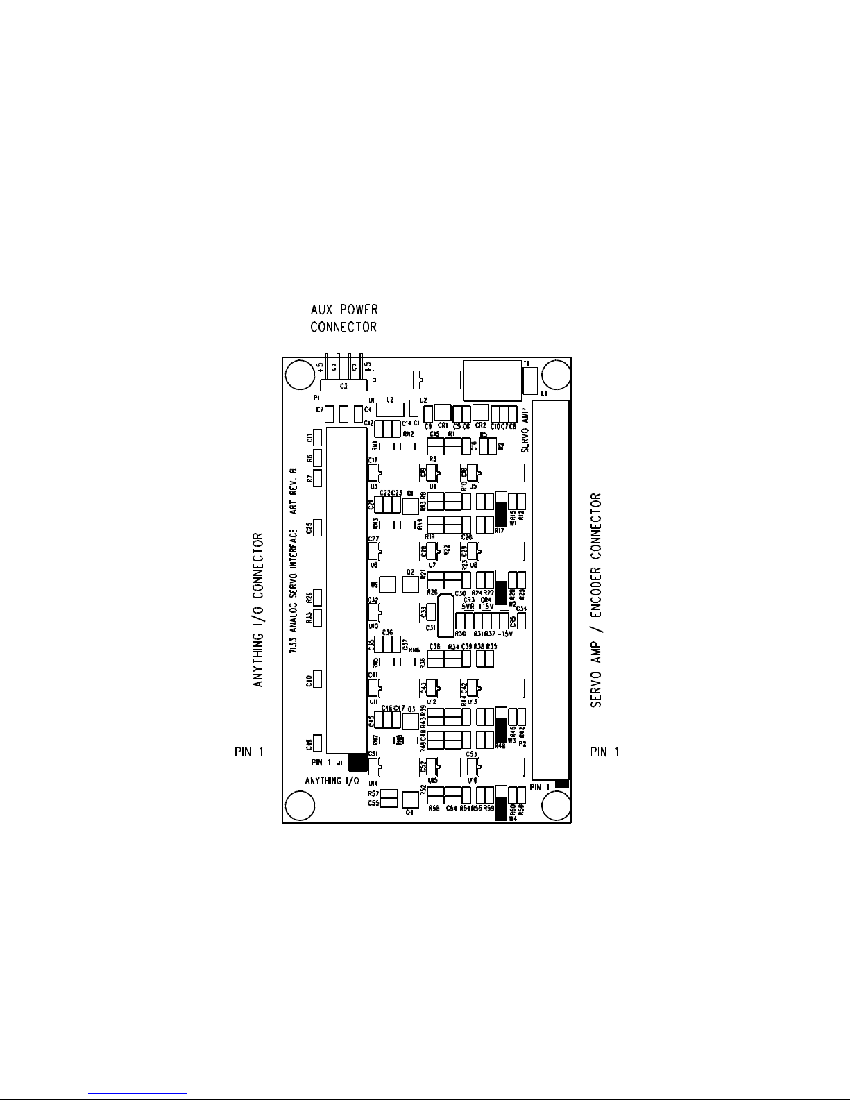
7I33 CONNECTOR LOCATIONS AND DEFAULT JUMPER POSITIONS
Page 7
7I33 4
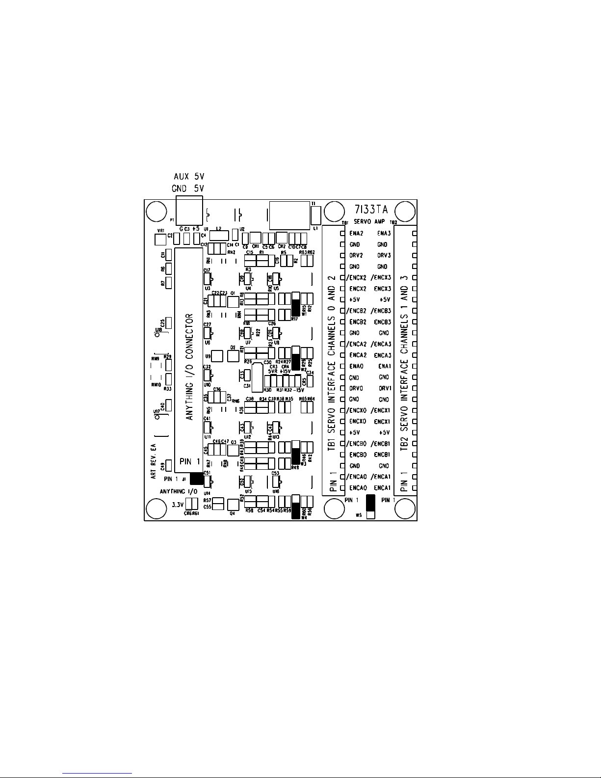
7I33TA CONNECTOR LOCATIONS AND DEFAULT JUMPER POSITIONS
Page 8

7I33 5
CONNECTORS
CONTROLLER CONNECTOR
50 pin header connector J1 connects to the anything I/O card/motion controller. This
can be a male 50 pin header on the top of the 7I33 card or a female 50 conductor header
on the bottom side of the 7I33 depending on 7I33 model. The controller connector pin-out
matches the 4I34M, 4I65, 4I68, 7I43, 7I60, 5I20, 5I22, 5I23 (4 axis) pinouts. Controller
connector pin-out is as follows:
PIN FUNCTION DIRECTION PIN FUNCTION DIRECTION
1 QB1 FROM 7I33 25 QB3 FROM 7I33
3 QA1 FROM 7I33 27 QA3 FROM 7I33
5 QB0 FROM 7I33 29 QB2 FROM 7I33
7 QA0 FROM 7I33 31 QA2 FROM 7I33
9 QX1 FROM 7I33 33 QX3 FROM 7I33
11 QX0 FROM 7I33 35 QX2 FROM 7I33
13 PWM1 TO 7I33 37 PWM3 TO 7I33
15 PWM0 TO 7I33 39 PWM2 TO 7I33
17 DIR1 TO 7I33 41 DIR3 TO 7I33
19 DIR0 TO 7I33 43 DIR2 TO 7I33
21 /ENA1 TO 7I33 45 /ENA3 TO 7I33
23 /ENA0 TO 7I33 47 /ENA2 TO 7I33
49 +5V PWR TO 7I33
Note: all even pins are grounded.
AUX 5V POWER
4 pin header P1 or 2 pin terminal block P1 can be used to supply 5V power to the 7I33 if
the controller cable is too long and voltage drop too high. P1 has the following pinout:
PIN FUNCTION (Rev. D and earlier) PIN FUNCTION (Rev. E and later)
1 5V 1 5V (Square pad)
2 GND 2 GND
3 GND
4 5V
Page 9

7I33 6
CONNECTORS
50 PIN SERVO AMP/ENCODER CONNECTOR
The 7I33s servo amplifier / encoder connector (P2) is a 50 pin latching header. P2 has the
following pinout:
PIN FUNCTION DIRECTION PIN FUNCTION DIRECTION
1 GND 26 ENCA2 TO 7I33
2 ENCA0 TO 7I33 27 /ENCA2 TO 7I33
3 /ENCA0 TO 7I33 28 GND
4 GND 29 ENCB2 TO 7I33
5 ENCB0 TO 7I33 30 /ENCB2 TO 7I33
6 /ENCB0 TO 7I33 31 VCC FROM 7I33
7 VCC FROM 7I33 32 IDX2 TO 7I33
8 ENCX0 TO 7I33 33 /IDX2 TO 7I33
9 /ENCX0 TO 7I33 34 GND
10 GND 35 DRV2 FROM 7I33
11 DRV0 FROM 7I33 36 GND
12 GND 37 ENA2 FROM 7I33
13 ENA0 FROM 7I33 38 ENCA3 TO 7I33
14 ENCA1 TO 7I33 39 /ENCA3 TO 7I33
15 /ENCA1 TO 7I33 40 GND
16 GND 41 ENCB3 TO 7I33
17 ENCB1 TO 7I33 42 /ENCB3 TO 7I33
18 /ENCB1 TO 7I33 43 VCC FROM 7I33
19 VCC 44 ENCX3 TO 7I33
20 ENCX1 TO 7I33 45 /ENCX3 TO 7I33
21 /ENCX1 TO 7I33 46 GND
22 GND 47 DRV3 FROM 7I33
23 DRV1 FROM 7I33 48 GND
24 GND 49 ENA3 FROM 7I33
25 ENA1 FROM 7I33 50 GND
Page 10

7I33 7
CONNECTORS
TERMINAL BLOCK SERVO AMP/ENCODER CONNECTORS
The 7I33TAs servo amplifier / encoder connectors (TB1 and TB2) are 3.5MM 24 pin
headers compatible with Phoenix pluggable terminal blocks (supplied with 7I33TA). TB1
(inner terminal block) pinout is as follows:
TB1 PIN SIGNAL DIRECTION FUNCTION
1 ENCA0 TO 7I33TA ENCODER 0 QUAD A
2 /ENCA0 TO 7I33TA ENCODER 0 INVERTED QUAD A
3 GND FROM 7I33TA ENCODER 0 GROUND
4 ENCB0 TO 7I33TA ENCODER 0 QUAD B
5 /ENCB0 TO 7I33TA ENCODER 0 INVERTED QUAD B
6 +5V FROM 7I33TA ENCODER 0 5V POWER
7 ENCX0 TO 7I33TA ENCODER 0 INDEX
8 /ENCX0 TO 7I33TA ENCODER 0 INVERTED INDEX
9 GND FROM 7I33TA ANALOG 0 GROUND
10 DRV0 FROM 7I33TA ANALOG 0 OUT
11 GND FROM 7I33TA SHIELD GND
12 ENA0 FROM 7I33TA ENABLE 0 OUT
13 ENCA2 TO 7I33TA ENCODER 2 QUAD A
14 /ENCA2 TO 7I33TA ENCODER 2 INVERTED QUAD A
15 GND FROM 7I33TA ENCODER 2 GROUND
16 ENCB2 TO 7I33TA ENCODER 2 QUAD B
17 /ENCB2 TO 7I33TA ENCODER 2 INVERTED QUAD B
18 +5V FROM 7I33TA ENCODER 2 5V POWER
19 ENCX2 TO 7I33TA ENCODER 2 INDEX
20 /ENCX2 TO 7I33TA ENCODER 2 INVERTED INDEX
21 GND FROM 7I33TA ANALOG 2 GROUND
22 DRV2 FROM 7I33TA ANALOG 2 OUT
23 GND FROM 7I33TA SHIELD GND
24 ENA2 FROM 7I33TA ENABLE 2 OUT
Page 11

7I33 8
CONNECTORS
TERMINAL BLOCK SERVO AMP/ENCODER CONNECTORS
TB2 (outer terminal block) pinout is as follows:
TB2 PIN SIGNAL DIRECTION FUNCTION
1 ENCA1 TO 7I33TA ENCODER 1 QUAD A
2 /ENCA1 TO 7I33TA ENCODER 1 INVERTED QUAD A
3 GND FROM 7I33TA ENCODER 1 GROUND
4 ENCB1 TO 7I33TA ENCODER 1 QUAD B
5 /ENCB1 TO 7I33TA ENCODER 1 INVERTED QUAD B
6 +5V FROM 7I33TA ENCODER 1 5V POWER
7 ENCX1 TO 7I33TA ENCODER 1 INDEX
8 /ENCX1 TO 7I33TA ENCODER 1 INVERTED INDEX
9 GND FROM 7I33TA ANALOG 1 GROUND
10 DRV1 FROM 7I33TA ANALOG 1 OUT
11 GND FROM 7I33TA SHIELD GND
12 ENA1 FROM 7I33TA ENABLE 1 OUT
13 ENCA3 TO 7I33TA ENCODER 3 QUAD A
14 /ENCA3 TO 7I33TA ENCODER 3 INVERTED QUAD A
15 GND FROM 7I33TA ENCODER 3 GROUND
16 ENCB3 TO 7I33TA ENCODER 3 QUAD B
17 /ENCB3 TO 7I33TA ENCODER 3 INVERTED QUAD B
18 +5V FROM 7I33TA ENCODER 3 5V POWER
19 ENCX3 TO 7I33TA ENCODER 3 INDEX
20 /ENCX3 TO 7I33TA ENCODER 3 INVERTED INDEX
21 GND FROM 7I33TA ANALOG 3 GROUND
22 DRV3 FROM 7I33TA ANALOG 3 OUT
23 GND FROM 7I33TA SHIELD GND
24 ENA3 FROM 7I33TA ENABLE 3 OUT
Page 12

7I33 9
OPERATION
PWM RATE
The 7I33 is meant to operate with PWM rates from 100 KHz to 10 MHz. Operation
at lower PWM rates will result in excessive output ripple . When used with SOFTDMC
firmware, it is best to set the PWM rate to the maximum (192 KHz). If the motion control
firmware is capable of generating interleaved PWM, that option should be enabled to
minimize output ripple. When used with HostMot2 firmware, the PWM generators PDM
option should be chosen with a frequency of 6 MHz. This will result in the best ripple and
linearity.
STEP RESPONSE
The 7I33 PWM filter has an approximate 150 uSec time constant. This value is
selected as a compromise between output ripple and settling time. This is much faster than
most controlled devices and will not normally have any effect on loop stability or
performance. The 7I33 can be assembled with different components if necessary to change
this time constant.
ENCODER INPUT CIRCUIT
The 7I33 input circuit is different depending on whether TTL or RS-422 encoder
types have been selected.
In TTL mode the input circuit on the encoder A,B, and Index inputs (ENCA, ENCB
and ENCX) consists of a RC filter followed by a Schmitt trigger. This helps to reject spike
noise on the encoder lines. The input circuit inverts the signals, so, for example, an active
high index signal will be active low at the controller interface.
In RS-422 mode, the input consists of true and inverted signals for each A,B and
index signal (ENCA, /ENCA, for A, ENCB, /ENCB for B and ENCX,/ENCX for index). The
RS-422 inputs have a 132 Ohm termination resistor across each true/inverted signal pair
and a 26LS32 RS-422 differential receiver.
MAXIMUM COUNT RATE
In TTL mode, the input RC filter limits the maximum encoder input frequency to
approximately 1 MHz. This corresponds to 4 million counts per second with most
quadrature counters (4X mode). The maximum input frequency may be lower with encoders
that have high value (>1K Ohm) pull-up resistors on open collector outputs.
In RS-422 mode, maximum encoder input frequency is 10 MHz, giving a maximum
count rate of 40 million counts per second. Maximum count rate may be further limited by
encoder counter limitations or rate filters.
Page 13

7I33 10
OPERATION
5V POWER
The 7I33 requires ~150 mA of 5V power for operation. Encoder power can also be
supplied from the 7I33's 5V source. Power for the 7I33 is normally supplied from pin 49 of
the 50 conductor controller cable, but can also be supplied via P1.
ENABLE INPUT
Each 7I33 channel has an active low TTL level enable input. When this input is high,
the corresponding AOUT is forced to 0V regardless of the state of the PWM and direction
inputs. A pullup resistor keeps the enable input high if the controller connection is lost.
ENABLE OUTPUT
Each 7I33 channel has an 5V CMOS active high enable output available on the
SERVO AMP / ENCODER connector. These signals are the logical inversion of the Enable
inputs.
ANALOG OUTPUT
The analog outputs (DRV 0 through 3) of the 7I33 swing from -10 v to +10V. Positive
outputs are generated when the DIR input is high, and negative outputs when DIR is low.
A 50 % duty cycle PWM signal will generate a 5V output. This mode of operation is often
referred to as sign-magnitude.
Due to power supply limitations, The 7I33 has limited DC output drive capability and
should not have loads of less than 5K Ohms on its analog outputs.
ANALOG DRIVE CONNECTIONS
Normally motor drives have differential inputs to reduce noise on their analog inputs.
To make the best use of this feature, the 7I33 should be wired to the drive with shielded
twisted pair wiring. Different drives have different input signal names, but typical
connections are 7I33 DRV to drive INPUT+, 7I33 GND (adjacent to DRV) to drive INPUT(these two signals are the twisted pair). The twisted pair shield should be terminated at the
7I33 ground and left un-terminated at the drive end. The drives input ground should be
returned to the same ground as the controller or PC,
Page 14

7I33 11
SPECIFICATIONS
MIN MAX UNITS
5V POWER SUPPLY 4.75 5.25 VDC
5V POWER CONSUMPTION --- 100 mA
(no external load)
ANALOG OUTPUT VOLTAGE +-9.7 +-10.3 V
MINIMUM AOUT LOAD RESISTANCE 5K --- Ohm
OUTPUT RIPPLE @ 100 KHZ PWM --- 2 % FS
OUTPUT RIPPLE @ 6 MHz PDM --- .2% % FS
LINEARITY (PWM or PDM) --- .2% % FS
ENCODER FREQUENCY (TTL) DC 1 MHz
ENCODER FREQUENCY (RS-422) DC 10 MHz
OPERATING TEMP. 0 +70
o
C
OPERATING TEMP. (-I version) -40 +85
o
C
OPERATION HUMIDITY 0 95% NON-COND
Page 15
7I33 12
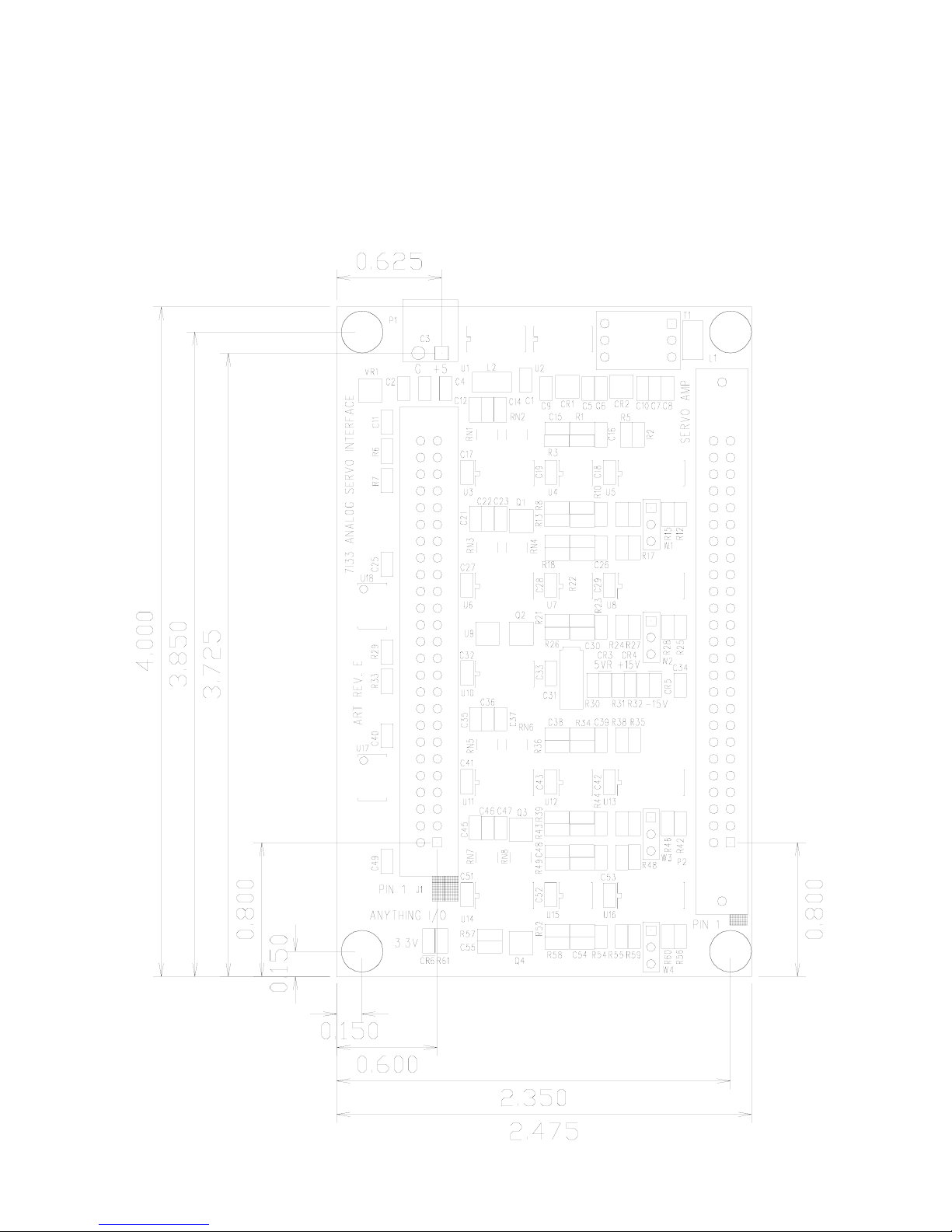
DRAWINGS
Page 16

7I33 13
DRAWINGS
 Loading...