

Page 1

4C81 MANUAL
Version 2.1
Page 2

Page 3

Table of Contents
GENERAL . . . . . . . . . . . . . . . . . . . . . . . . . . . . . . . . . . . . . . . . . . . . . . . . . . . . . . . . . . 1
DESCRIPTION . . . . . . . . . . . . . . . . . . . . . . . . . . . . . . . . . . . . . . . . . . . . . . . . . 1
HARDWARE CONFIGURATION . . . . . . . . . . . . . . . . . . . . . . . . . . . . . . . . . . . . . . . . . 2
GENERAL . . . . . . . . . . . . . . . . . . . . . . . . . . . . . . . . . . . . . . . . . . . . . . . . . . . . . 2
BOOT OPTION . . . . . . . . . . . . . . . . . . . . . . . . . . . . . . . . . . . . . . . . . . . . . . . . . 2
FPGA/CPLD LVTTL CONNECTOR POWER . . . . . . . . . . . . . . . . . . . . . . . . . . 2
FPGA/CPLD LVTTL OUTPUT VCC . . . . . . . . . . . . . . . . . . . . . . . . . . . . . . . . . . 2
NAND FLASH WRITE PROTECT . . . . . . . . . . . . . . . . . . . . . . . . . . . . . . . . . . . 2
CONNECTORS . . . . . . . . . . . . . . . . . . . . . . . . . . . . . . . . . . . . . . . . . . . . . . . . . . . . . . 3
CONNECTOR AND DEFAULT JUMPER LOCATIONS . . . . . . . . . . . . . . . . . . . 3
POWER/SERIAL CONSOLE CONNECTOR . . . . . . . . . . . . . . . . . . . . . . . . . . 4
4C81 SERIAL ADAPTER . . . . . . . . . . . . . . . . . . . . . . . . . . . . . . . . . . . . . . . . . . 4
FPGA/CPLD LVTTL CONNECTOR . . . . . . . . . . . . . . . . . . . . . . . . . . . . . . . . . . 5
FPGA/CPLD LVDS CONNECTOR . . . . . . . . . . . . . . . . . . . . . . . . . . . . . . . . . . 6
ETHERNET CONNECTORS . . . . . . . . . . . . . . . . . . . . . . . . . . . . . . . . . . . . . . . 6
JTAG CONNECTOR . . . . . . . . . . . . . . . . . . . . . . . . . . . . . . . . . . . . . . . . . . . . . 7
CPU OPERATION . . . . . . . . . . . . . . . . . . . . . . . . . . . . . . . . . . . . . . . . . . . . . . . . . . . . 8
POWER . . . . . . . . . . . . . . . . . . . . . . . . . . . . . . . . . . . . . . . . . . . . . . . . . . . . . . . 8
SERIAL CONSOLE . . . . . . . . . . . . . . . . . . . . . . . . . . . . . . . . . . . . . . . . . . . . . . 8
PC/104-PCI EXPANSION . . . . . . . . . . . . . . . . . . . . . . . . . . . . . . . . . . . . . . . . . 8
MINI PCI EXPANSION . . . . . . . . . . . . . . . . . . . . . . . . . . . . . . . . . . . . . . . . . . . 8
ETHERNET PORTS . . . . . . . . . . . . . . . . . . . . . . . . . . . . . . . . . . . . . . . . . . . . . 8
GPIO BITS . . . . . . . . . . . . . . . . . . . . . . . . . . . . . . . . . . . . . . . . . . . . . . . . . . . . . 9
FPGA OPTION . . . . . . . . . . . . . . . . . . . . . . . . . . . . . . . . . . . . . . . . . . . . . . . . 10
FPGA/CPU CONNECTIONS . . . . . . . . . . . . . . . . . . . . . . . . . . . . . . . . . . . . . . 10
FPGA CONFIGURATION . . . . . . . . . . . . . . . . . . . . . . . . . . . . . . . . . . . . . . . . 11
EXAMPLE FPGA CONFIG FILE . . . . . . . . . . . . . . . . . . . . . . . . . . . . . . . . . . . 12
P4 PINOUT WITH EXAMPLE FPGA CONFIGURATION . . . . . . . . . . . . . . . . 12
P3 PINOUT WITH EXAMPLE FPGA CONFIGURATION . . . . . . . . . . . . . . . . 13
FPGAPOKE UTILITY . . . . . . . . . . . . . . . . . . . . . . . . . . . . . . . . . . . . . . . . . . . . 13
CPLD I/O . . . . . . . . . . . . . . . . . . . . . . . . . . . . . . . . . . . . . . . . . . . . . . . . . . . . . 14
CPLD CPU INTERFACE . . . . . . . . . . . . . . . . . . . . . . . . . . . . . . . . . . . . . . . . . 14
STANDARD CPLD CONFIGURATION . . . . . . . . . . . . . . . . . . . . . . . . . . . . . . 15
P4 PINOUT WITH STANDARD CPLD CONFIGURATION . . . . . . . . . . . . . . . 15
P3 PINOUT WITH STANDARD CPLD CONFIGURATION . . . . . . . . . . . . . . . 16
CPLD JTAG PINOUT . . . . . . . . . . . . . . . . . . . . . . . . . . . . . . . . . . . . . . . . . . . . 16
iii
Page 4

Table of Contents
SOFTWARE
GENERAL . . . . . . . . . . . . . . . . . . . . . . . . . . . . . . . . . . . . . . . . . . . . . . . . . . . . . 17
BOOTLOADER . . . . . . . . . . . . . . . . . . . . . . . . . . . . . . . . . . . . . . . . . . . . . . . . . 17
NET BOOT REQUIREMENTS . . . . . . . . . . . . . . . . . . . . . . . . . . . . . . . . . . . . . . 18
NETBSD SOFTWARE
GENERAL . . . . . . . . . . . . . . . . . . . . . . . . . . . . . . . . . . . . . . . . . . . . . . . . . . . . . 19
REMOTE FILE ACCESS . . . . . . . . . . . . . . . . . . . . . . . . . . . . . . . . . . . . . . . . . . 19
BOOT ROM UPDATING . . . . . . . . . . . . . . . . . . . . . . . . . . . . . . . . . . . . . . . . . . 19
NAND FLASH UPDATING . . . . . . . . . . . . . . . . . . . . . . . . . . . . . . . . . . . . . . . . . 20
NETBSD NAND FLASH IMAGE . . . . . . . . . . . . . . . . . . . . . . . . . . . . . . . . . . . . 21
CHANGING NAND FLASH FILESYSTEM MODE . . . . . . . . . . . . . . . . . . . . . . . 21
CHANGING PASSWORDS . . . . . . . . . . . . . . . . . . . . . . . . . . . . . . . . . . . . . . . . 21
ENABLING SSHD . . . . . . . . . . . . . . . . . . . . . . . . . . . . . . . . . . . . . . . . . . . . . . . 22
CHANGING PASSWORDS . . . . . . . . . . . . . . . . . . . . . . . . . . . . . . . . . . . . . . . . 22
NETBSD NET BOOT BINARY DISTRIBUTION . . . . . . . . . . . . . . . . . . . . . . . . 22
NETBSD TOOLCHAIN . . . . . . . . . . . . . . . . . . . . . . . . . . . . . . . . . . . . . . . . . . . 23
LINUX SOFTWARE . . . . . . . . . . . . . . . . . . . . . . . . . . . . . . . . . . . . . . . . . . . . . . . . . . . 24
GENERAL . . . . . . . . . . . . . . . . . . . . . . . . . . . . . . . . . . . . . . . . . . . . . . . . . . . . . 24
KERNEL BOOT OPTIONS . . . . . . . . . . . . . . . . . . . . . . . . . . . . . . . . . . . . . . . . 24
SEEPROM . . . . . . . . . . . . . . . . . . . . . . . . . . . . . . . . . . . . . . . . . . . . . . . . . . . . . 24
KCMD/NETKCMD . . . . . . . . . . . . . . . . . . . . . . . . . . . . . . . . . . . . . . . . . . . . . . . 24
SPECIFICATIONS . . . . . . . . . . . . . . . . . . . . . . . . . . . . . . . . . . . . . . . . . . . . . . . . . . . . 26
iv
Page 5

GENERAL
DESCRIPTION
The 4C81 is a low cost, low power ARM based PC104-PCI CPU. Designed for
networked applications, the 4C81 has two 10/100 baseT Ethernet interfaces and a slot for
a WI-FI card or other Mini-PCI device. The 166 MHz CPU card consumes less than 2 watts
total from a single 5V supply, making Solar powered applications practical.
System resources include 32M or 64M of RAM and 32M or more of NAND Flash
memory, 36 I/O bits provided by either a CPLD or an FPGA and an RS-232 serial port.
PC/104-PCI expansion is provided for up to 2 external bus master cards. The Ethernet
interfaces generates hardware TCP checksums allowing close to wire speed routing
through the 4C81.
An optional on card 200K or 400K gate Spartan3 FPGA with 32 bit local bus
connection provides flexible user I/O or a custom processing accelerator. The FPGA has
36 User I/O pins available, 24 single ended LVTTL I/O bits on a standard 50 pin header with
interleaved grounds, and 12 I/O bits on a 20 pin 2MM header organized as 6 LVDS pairs
with grounds between pairs.
The 4C81 can run Linux or NetBSD and has a jumper selectable netboot option with
NFS support to allow simple system debug and software development.
4C81 MANUAL 1
Page 6

HARDWARE CONFIGURATION
GENERAL
Jumper positions are specified with an upright card orientation. The 4C81 is upright
when the top of the card (connector side) faces you, the PC/104-PLUS connector is away
from you and the Ethernet connectors are on the right hand side.
NETBOOT OPTION
The 4C81 can boot from its on card NAND flash or can netboot from a remote NFS
server. This is useful in case the NAND flash becomes corrupted and for initial setup. W8
determines whether the 4C81 boots from the on card NAND flash chip or attempts a
network boot. When W8 is in the right hand position, the 4C81 will boot from NAND flash.
When W8 is in the left hand position the 4C81 will attempt a net boot. Network boot is
always from Ethernet port 0.
FPGA LVTTL VCC
The I/O voltage for the FPGA pins that connect to the LVTTL connector can be user
selected. Jumper W7 selects the I/O voltage. When W7 is in the right hand position, the I/O
voltage is 2.5V. When W7 is in the left hand position, the I/O voltage is 3.3V.
FPGA LVTTL CONNECTOR POWER
The LVTTL connector can supply power to connected daughter cards. This power
can be either 3.3V or 5V. When jumper W9 is in the left hand position, 5V is supplied on pin
49 of the LVTTL I/O connector. When W9 is in the right hand position, 3.3V is supplied on
pin 49.
NAND FLASH WRITE PROTECT
The on card NAND flash can be protected against writes by removing jumper W3.
This will prevent any change of NAND flash contents.
4C81 MANUAL 2
Page 7
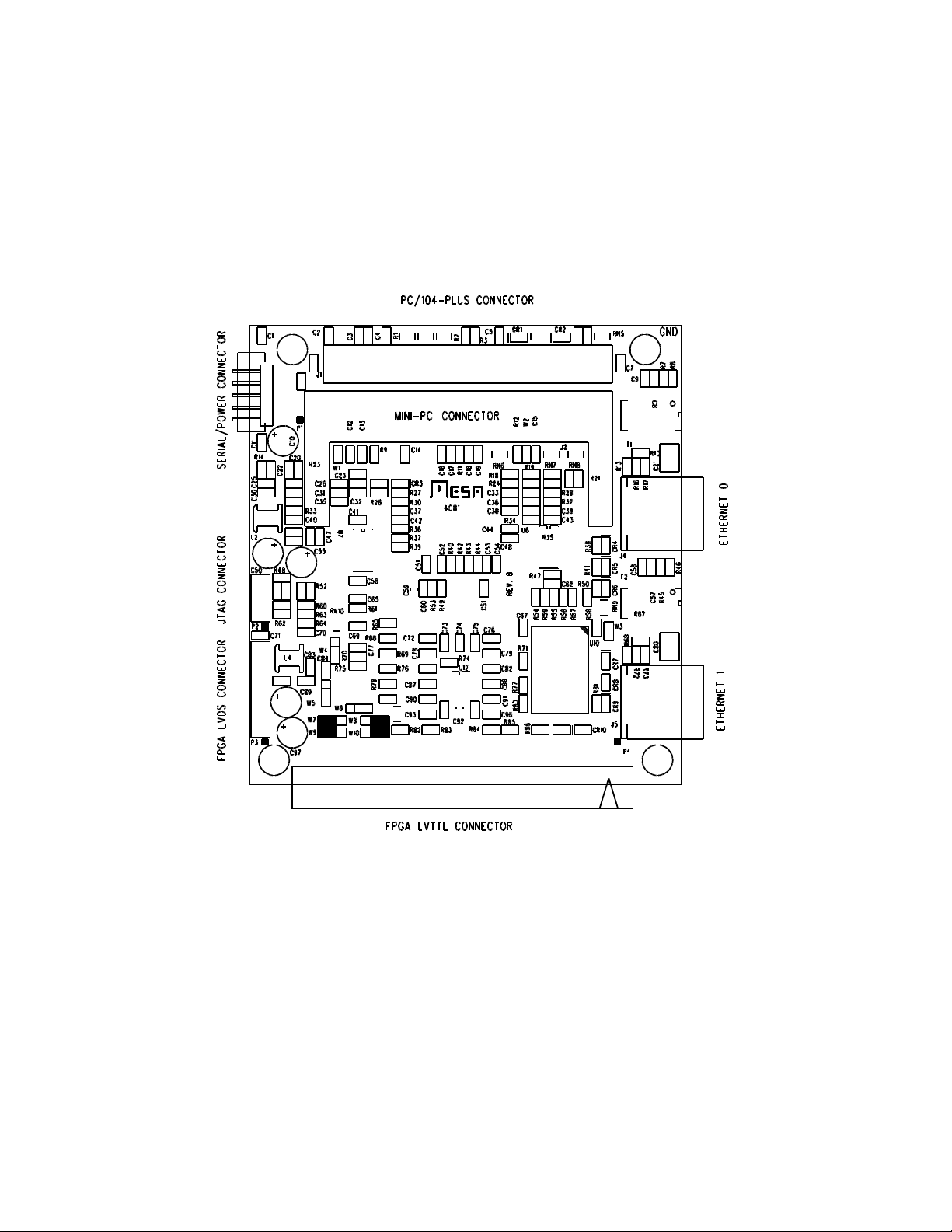
CONNECTORS
CONNECTOR AND DEFAULT JUMPER LOCATIONS
4C81 MANUAL 3
Page 8

CONNECTORS
SERIAL/POWER CONNECTOR
P1 is the serial console and power connector. Note that the first 6 pins match the
standard DE9 pin male (DTE) serial port pinout used on PC serial ports.
PIN FUNCTION DIRECTION
1 CD TO 4C81
2 DSR TO 4C81
3 RXD TO 4C81
4 RTS FROM 4C81
5 TXD FROM 4C81
6 CTS TO 4C81
7 +5V TO 4C81
8 GND TO 4C81
9 GND TO 4C81
10 +5V TO 4C81
4C81 SERIAL ADAPTER
The 4C81 serial adapter converts the DTE pinout of the 4C81 to DCE for direct
connection to PC type 9 pin serial ports, and also has a 4 pin .1" 5V power connector. The
5V connector on the serial adapter is pinned out as follows:
1 +5V
2 GND
3 GND
4 +5V
4C81 MANUAL 4
Page 9

CONNECTORS
FPGA/CPLD LVTTL CONNECTOR
P4 is the FPGA/CPLD LVTTL connector. P4 is a 50 pin .1" header. P4 is compatible
with Mesa’s Anything-I/O daughter cards with the restriction that FPGA I/O signals are not
5V tolerant. The CPLD I/O is 5V tolerant.
P4 CONNECTOR PINOUT
P4 PIN FUNC FPGA PIN P4 PIN FUNC FPGA PIN
1 IO0 77 3 IO1 78
5 IO2 79 7 IO3 80
9 IO4 82 11 IO5 83
13 IO6 84 15 IO7 85
17 IO8 86 19 IO9 87
21 IO10 89 23 IO11 90
25 IO12 92 27 IO13 93
29 IO14 95 31 IO15 96
33 IO16 97 35 IO17 98
37 IO18 99 39 IO19 100
41 IO20 102 43 IO21 103
45 IO22 104 47 IO23 105
49 POWER
All even pins are connected to ground.
The POWER pin can be connected to either 3.3V or 5V power depending on the
position of W7.
4C81 MANUAL 5
Page 10

CONNECTORS
FPGA/CPLD LVDS CONNECTOR
P3 is a 20 pin 2mm header that connects to 12 FPGA I/O pins intended for use as
a LVDS signals. P3 pinout is as follows:
P3 PIN FUNC FPGA PIN P3 PIN FUNC FPGA PIN
1 GND XX 11 LVDS3+ 127
2 LVDS0+ 118 12 LVDS3- 128
3 LVDS0- 119 13 GND XX
4 GND XX 14 LVDS4+ 129
5 LVDS1+ 122 15 LVDS4- 130
6 LVDS1- 123 16 GND XX
7 GND XX 17 LVDS5+ 131
8 LVDS2+ 124 18 LVDS5- 132
9 LVDS2- 125 19 GND XX
10 GND XX 20 +3.3V XX
Note that The DCI (internal termination) feature does not work properly on Rev.A
cards so if the LVDS feature is used, External termination must be supplied. This is fixed
on card rev. B and above. CPLD versions of the 4C81 provide 12 I/O bits on the LVDS pins.
ETHERNET CONNECTORS
The 4C81 has 2 Ethernet ports. Port 0 and Port 1. Port 0 is the port closest to the
PC/104-PLUS connector. Both ports are standard RJ45 jacks. Low profile unshielded jacks
are used in order to meet the PC/104 component height specifications.
4C81 MANUAL 6
Page 11

CONNECTORS
JTAG CONNECTOR
P2 is a 10 pin 2mm connector that gives access to the JTAG boundary scan chain
on the 4C81s CPU and FPGA.. P2 connector pinout is as follows:
PIN FUNCTION DIR
1 TMS TO 4C81
2 TDI TO 4C81
3 TDO FROM 4C81
4 TCK TO 4C81
5 /RST TO 4C81
6 GND
7 2.5V
8 /ROMCS TO 4C81 (test mode only)
9 /ROMOE TO 4C81 (test mode only)
10 /ROMWE TO 4C81 (test mode only)
4C81 MANUAL 7
Page 12

CPU OPERATION
POWER
Power is supplied to the 4C81 via the serial console/power connector or the PC/104PLUS bus. The 4C81 requires 5V power only. If 5V is not required for the PC/104-PLUS bus
or a Mini-PCI card, the 5V supply can vary from 4V to 5V, as no 5V power is used on the
4C81 itself. If +12V and or -12V power are required by a PC/104-PLUS card, these must
be supplied via the PC/104-PLUS bus.
SERIAL CONSOLE
The 4C81 has a single serial port that is used as console I/O by the boot ROM and
Linux or NetBSD. The default communication parameters are: 38400 baud, 8 bits, no parity.
Note that the serial console pinout is DTE so that a null modem is required to connect the
4C81s console to A PC terminal emulator. A Null modem adapter is available from Mesa
(NullModemX). This adapter also has the 5V power tap to simplify powering the 4C81.
PC/104-PCI EXPANSION
The 4C81 is a PC/104-PCI card and can accept PC/104-PCI expansion cards. The
4C81 has a 3.3V PCI bus and will only work properly with 3.3V or universal PC/104-PCI
cards. 5V cards are not supported and may damage the 4C81. Two bus master cards
are supported: slots 1, and 2. Slot 0 is reserved for the Mini-PCI card. A non bus master
card can be accommodated in slot 3.
The 4C81 on card regulator can supply up to 1.5A of 3.3V power to the PC/104-PCI bus.
MINI-PCI EXPANSION
A single Mini-PCI type 3A socket is provided for wireless and other Mini-PCI
cards. This socket is slot 0 of the PCI expansion bus.
ETHERNET PORTS
Two 10/100 BaseT Ethernet ports are provided. These ports support full duplex
for high performance and auto-MDX for wiring simplicity. Three surface mount LEDS are
provided on each port to monitor link status.
4C81 MANUAL 8
Page 13

CPU OPERATION
CPU GPIO BITS
The 4C81 CPU chip has 16 GPIO bits that are used for various on card functions.
The bit definitions are as follows:
GPIO-0 INPUT PCI INTERRUPT
GPIO-1 INPUT WLAN RFON SENSE
GPIO-2 INPUT FPGA/CPLD IRQ
GPIO-3 OUTPUT KSE0 ACTIVITY
GPIO-4 OUTPUT KSE1 ACTIVITY
GPIO-5 OUTPUT SERIAL EEPROM CHIP SELECT
GPIO-6 OUTPUT GREEN LED CR3
GPIO-7 OUTPUT FPGA /PWREN
GPIO-8 OUTPUT NOR FLASH A22 (4M PAGE BIT)
GPIO-9 INPUT NAND FLASH RDY/BUSY
GPIO-10 OUTPUT FPGA /PROGRAM
GPIO-11 INPUT FPGA /DONE SENSE
GPIO-12 OUTPUT NAND FLASH CE
GPIO-13 I/O EEPROM CLK C W8 SENSE
GPIO-14 I/O EEPROM DI C W10 SENSE
GPIO-15 I/O EEPROM DO B W6,W11 SENSE
4C81 MANUAL 9
Page 14

CPU OPERATION
FPGA OPTION
The 4C81 can be provided with an on card Spartan3 FPGA with 200K or 400K gates.
This FPGA can be used for custom I/O or a co-processor. 36 uncommitted FPGA I/O bits
are available for user applications. 24 of these I/O bits are designed for single ended 3.3V
or 2.5V LVTTL applications and 12 are designed for differential 2.5V LVDS applications.
FPGA CPU INTERFACE
The FPGA connects to the 4C81 CPUs 32 bit data bus. 9 addresses are connected
to the FPGA giving a address span of 512 32 bit words. In addition the FPGA connects to
CPU /ECS0 and read and write strobes.
CPU SIG FPGA PIN DIR CPU SIG FPGA PIN DIR
MD0 65 BIDIR MD13 7 BIDIR
MD1 63 BIDIR MD14 8 BIDIR
MD2 60 BIDIR MD15 10 BIDIR
MD3 59 BIDIR MD16 11 BIDIR
MD4 51 BIDIR MD17 12 BIDIR
MD5 50 BIDIR MD18 13 BIDIR
MD6 47 BIDIR MD19 14 BIDIR
MD7 46 BIDIR MD20 15 BIDIR
MD8 1 BIDIR MD21 17 BIDIR
MD9 2 BIDIR MD22 18 BIDIR
MD10 4 BIDIR MD23 20 BIDIR
MD11 5 BIDIR MD24 21 BIDIR
MD12 6 BIDIR MD25 23 BIDIR
4C81 MANUAL 10
Page 15

CPU OPERATION
FPGA CPU INTERFACE
CPU SIG FPGA PIN DIR CPU SIG FPGA PIN DIR
MD26 24 BIDIR MA6 36 TO FPGA
MD27 25 BIDIR MA7 44 TO FPGA
MD28 26 BIDIR MA8 56 TO FPGA
MD29 27 BIDIR MA9 57 TO FPGA
MD30 28 BIDIR MA10 68 TO FPGA
MD31 30 BIDIR ECSN0 40 TO FPGA
MA2 31 TO FPGA EROEN 53 TO FPGA
MA3 32 TO FPGA ERWEN0 52 TO FPGA
MA4 33 TO FPGA CLK 55 TO FPGA
MA5 35 TO FPGA LED 58 FROM FPGA
Notes: FPGA clock is normally the same as the SDRAM clock = 125 MHz.
LED is green LED CR10 on the bottom right hand side of the 4C81 card
FPGA CONFIGURATION
The FPGA is configured by writing the bit file to the memory region defined for
ECSN0. The address is unimportant as long as it is word aligned and in the FPGAMEM
region.
Two processor GPIO bits are used by the FPGA interface, GPIO10 and GPIO11.
GPIO10 is programmed as an output bit and controls the /PROGRAM pin of the FPGA
GPIO10 must be set low and then high again to prepare the FPGA to receive the
configuration file. GPIO11 is programmed as an input and read backs the FPGAs done bit.
The DONE bit will read high when the FPGA has been successfully configured.
The included FPGAUTIL will configure the 4C81's FPGA from a bit or PROM format
file:
FPGAUTIL fourc81io.bit
4C81 MANUAL 11
Page 16

CPU OPERATION
EXAMPLE FPGA CONFIGURATION FILE
An example FPGA configuration file (fourc81io.bit) is provided that includes 4 timers and
36 bits of I/O. The I/O is divided into two ports, a 24 bit port connected to P4 and a 12 bit
port connected to P3. Each I/O bit can be individually programmed as an input or output.
The timers are 32 bit down counters that can be read on-the-fly. The count rate is
determined by a 32 bit DDS oscillator running at 125 MHz, allowing precise count rate
settability. Each counter can generate an interrupt. The counters can operate in free running
or one shot mode. In one shot mode, the counters can be programmed to drive an I/O pin.
VHDL source and .UCF files for the example are provided with the software
distribution image for the 4C81. A detailed register map of the example configuration is
provided in the file 4c81ioregisters.
P4 PINOUT WITH EXAMPLE FPGA CONFIGURATION
P1 PORTA0/TIMER0 OUT P3 PORTA1/TIMER 1 OUT
P5 PORTA2/TIMER 2 OUT P7 PORTA3/TIMER 3 OUT
P9 PORTA4 P11 PORTA5
P13 PORTA6 P15 PORTA7
P17 PORTA8 P19 PORTA9
P21 PORTA10 P23 PORTA11
P25 PORTA12 P27 PORTA13
P29 PORTA14 P31 PORTA15
P33 PORTA16 P35 PORTA17
P37 PORTA18 P39 PORTA19
P41 PORTA20 P43 PORTA21
P45 PORTA22 P47 PORTA23
P49 5V OR 3.3V ALL EVEN PINS GROUNDED
4C81 MANUAL 12
Page 17

CPU OPERATION
EXAMPLE FPGA CONFIGURATION
P3 PINOUT WITH EXAMPLE FPGA CONFIGURATION:
P1 GND P2 PORTB0
P3 PORTB1 P4 GND
P5 PORTB2 P6 PORTB3
P7 GND P8 PORTB4
P9 PORTB5 P10 GND
P11 PORTB6 P12 PORTB7
P13 GND P14 PORTB8
P15 PORTB9 P16 GND
P17 PORTB10 P18 PORTB11
P19 GND P20 +3.3V
FPGAPOKE UTILITY
The FPGAPOKE utililty allows direct access to FPGA registers for debugging.
FPGAPOKE must be run as root. For example, using the example FPGA configuration
provided:
FPGAPOKE -R 0x00 -g
Would read the FPGA configuration ID register (0x4c810001 for the example configuration)
FPGAPOKE -R 0x24 0x00ffffff -s
Would set 24 bit IO PORTA’s DDR register so that all I/O pins were programmed as
outputs.
FPGAPOKE -R 0x20 0x00aaaaaa -s
Would set the 24 output bits to alternate 1's and 0's
4C81 MANUAL 13
Page 18

CPU OPERATION
CPLD I/O
The 4C81-N (without FPGA option) has a simple CPLD to provide 36 GPIO bits or
other custom IO pins on connectors P3 and P4.
CPLD CPU INTERFACE
The CPLD connects the low 16 bit half of the 4C81's 32 bit data bus. 6 addresses
are connected to the CPLD giving a address span of 64 16 bit words. In addition the CPLD
connects to CPU /ECS0, 125 MHz bus clock and read and write strobes, reset and CPU
GPIO2 which can be used as an interrupt.
CPU SIG CPLD PIN DIR CPU SIG CPLD PIN DIR
MD0 41 BIDIR MD1 40 BIDIR
MD2 39 BIDIR MD3 37 BIDIR
MD4 30 BIDIR MD5 32 BIDIR
MD6 33 BIDIR MD7 35 BIDIR
MD8 1 BIDIR MD9 3 BIDIR
MD10 4 BIDIR MD11 6 BIDIR
MD12 8 BIDIR MD13 9 BIDIR
MD14 10 BIDIR MD15 11 BIDIR
MA2 13 TO CPLD MA3 14 TO CPLD
MA4 15 TO CPLD MA5 16 TO CPLD
MA6 17 TO CPLD MA7 18 TO CPLD
/CS0 28 TO CPLD /OE0 29 TO CPLD
/WE0 27 TO CPLD CLK 22 TO CPLD
/RST 12 TO CPLD
4C81 MANUAL 14
Page 19

CPU OPERATION
STANDARD CPLD CONFIGURATION
The 4C81-N (without FPGA option) has a simple CPLD (Xilinx 9572XL-PQ100) to
provide 36 GPIO bits on connector P3 and P4. The standard CPLD configuration provides
36 I/O pins, 24 on P4, and 12 on P3. The 24 I/O bits on P4 can be individually programmed
as inputs or outputs. The I/O on P3 is more limited. The lower 6 bits are input only while
the top 6 bits can be programmed as all inputs or all output as a group.
P4 PINOUT WITH STANDARD CPLD CONFIGURATION
P1 PORTA0 P3 PORTA1
P5 PORTA2 P7 PORTA3
P9 PORTA4 P11 PORTA5
P13 PORTA6 P15 PORTA7
P17 PORTA8 P19 PORTA9
P21 PORTA10 P23 PORTA11
P25 PORTB0 P27 PORTB1
P29 PORTB2 P31 PORTB3
P33 PORTB4 P35 PORTB5
P37 PORTB6 P39 PORTB7
P41 PORTB8 P43 PORTB9
P45 PORTB10 P47 PORTB11
P49 5V OR 3.3V ALL EVEN PINS GROUNDED
4C81 MANUAL 15
Page 20

CPU OPERATION
P3 PINOUT WITH STANDARD CPLD CONFIGURATION:
P1 GND P2 PORTC0
P3 PORTC1 P4 GND
P5 PORTC2 P6 PORTC3
P7 GND P8 PORTC4
P9 PORTC5 P10 GND
P11 PORTC6 P12 PORTC7
P13 GND P14 PORTC8
P15 PORTC9 P16 GND
P17 PORTC10 P18 PORTC11
P19 GND P20 +3.3V
Note CPLD I/O pins use 3.3V levels (VOH ~= 3.3V) and are 5V tolerant.
CPLD JTAG CONNECTOR
The CPLD on the 4C81N can be re-programmed externally via JTAG connector P5.
P5 is a 6 pin inline .1" header. P5 pinout is as follows:
PIN SIGNAL PIN SIGNAL PIN SIGNAL
1 TMS 2 TDI 3 TDO
4 TCK 5 GND 6 3.3V
Note, to allow in circuit programming of the CPLD via the CPU, the CPLD’s JTAG
pins also connect to GPIO pins on the CPU. To avoid interference from the CPU while
externally programming the CPLD, the CPU should be held reset. This is easily done by
placing a 2mm jumper on pins 5 and 6 of CPU JTAG connector P2.
4C81 MANUAL 16
Page 21

SOFTWARE
GENERAL
The 4C81 can run NetBSD or Linux. The on card 32M byte NAND flash chip can
accommodate a small distribution of either operating system. The 4C81 can also be ordered
with either operating system pre-loaded on the NAND flash.
BOOTLOADER
The 4C81 bootloader ROM loads the NetBSD or Linux Kernel from either NAND
flash or from a server (NetBoot option). The netboot option is useful during software
development as it does not require re-writing the NAND flash when updating the kernel.
The netboot option can also be used to initialize the NAND flash on a 4C81 with a blank or
corrupted NAND flash image. Jumpers W8 and W10 determine the low level boot options:
W8 W10 FUNCTION
LEFT LEFT NET BOOT - IGNORE SERIAL EEPROM SETTINGS
This is for Factory setup (Uses default MAC addresses
and console baud rate etc) Default MAC address is:
00:60:1b:81:00:01 for KSE0 and 00:60:1b:81:00:02 for
KSE1
LEFT RIGHT NORMAL NET BOOT
Net boot with normal Ethernet MAC addresses
RIGHT LEFT DEBUG FLASH BOOT
RIGHT RIGHT NORMAL USER FLASH BOOT
4C81 MANUAL 17
Page 22

SOFTWARE
NETBOOT REQUIREMENTS
In order for the 4C81 to boot from the network, a NFS and a DHCP server must
present and properly configured. The DHCP server must be configured with boot options
in dhcpd.conf for the hardware address or address range of the 4C81(s)
For example:
host 4c81 {
hardware ethernet 00:60:1B:00:4C:81;
fixed-address 192.168.1.10;
server-name "myserver.mydomain.com";
option root-path "/mybootdir/4c81";
option host-name "4c81"; }
The netboot option uses NFS to fetch the kernel so the root path in the example
above must be exported, for example the following line in the exports file:
/mybootdir -alldirs -network 192.168.1 -mask 255.255.255.0
Would make the kernel available to the 4c81 as long as the kernel was readable and
located in /mybootdir/4c81/.
4C81 MANUAL 18
Page 23

NETBSD SOFTWARE
GENERAL
The NetBSD distribution for the 4C81 is a complete Unix with support for Atheros
Wireless cards, Ethernet, Local FPGA, and serial console.
REMOTE FILE ACCESS
In order to update the BOOT ROM or NAND flash image, the 4C81 needs access
to the new image files. For small files like the boot ROM, it is possible to FTP the new image
to a location in RAM disk (in /var for example) and then program the new image from there.
This will not work for NAND filesystem images since there is not enough free space in the
RAM disk to store the image. In order to write new NAND filesystem images you must have
either a NFS server or Windows file share (Samba) available. To mount the files system you
issue a command like:
mount -t nfs yourserver:/yourpath /mnt1 For NFS
or
mount -t smbfs //yourserver/yourpath /mnt1 For Windows share/SMBFS
BOOT ROM UPDATING
The 4C81 boot ROM is a NOR flash device. A utility (flashutil) is provided to update
the NOR flash boot ROM. Flashutil is invoked like this
flashutil bootfilename -W
Only root can run flashutil. Be careful that you update the flash with a legitimate
boot image, as a update with the wrong file will make an unbootable 4C81 that will
need to be returned to MESA for repair. All 4C81 boot images have a file name like
boot81.xxxk where xxx is the boot file image size.
4C81 MANUAL 19
Page 24

NETBSD SOFTWARE
NAND FLASH UPDATING
The NAND flash on the 4C81 is used as a live read-only file system. It contains the
operating system and utility programs. New NAND flash images can be written to the 4C81
with the nandstore utility. Nandstore should only be run when the 4C81 is net booted or
running in single user mode. To write a new NAND flash image, nandstore is invoked like
this:
/mesa/nandstore build=nandfilsystemimage
Only root can run nandstore.
To modify an existing NAND file system image, the image must first be mounted
using the vnd driver:
vnconfig /dev/vnd0 nandsfilesystemimage
mount /dev/vnd0c /mnt
Then the desired modification are made to the file system on /mnt. Next the file
system must flush any pending file writes with a sync command and then the file system
cam be unmounted:
sync
umount /mnt
Finally the updated file system image can be written to the NAND flash with
nandstore:
nandstore build=nandfilsystemimage
4C81 MANUAL 20
Page 25

NETBSD SOFTWARE
NETBSD NAND FLASH IMAGE
The 32MB NAND flash image uses approximately 22 MB of the flash chip, leaving
~10 MB free for user applications. The 64MB NAND flash image has approximately 40 MB
free. The images include a useful subset of full Unix system utilities. The kernel and NAND
flash support DHCP, IPV6, SSH, NFS ,SMBFS, Bridging interfaces, SH and KSH. The
NAND flash file system is read-only by default so any changes need to be made by
temporarily changing to RW mode or using the method described above for NAND FLASH
UPDATING.
CHANGING NAND FLASH FILESYSTEM MODE
In order to permanently change any program, script or file on the 4C81 NetBSD
NAND flash distribution, the filesystem must be temporarily be placed into R/W mode. There
are 2 scripts in the /mesa directory of the distribution that change the mode of the filesystem
to Read/Write and to Read/Only:
/mesa/nandfsrw Changes NAND filesystem mode to Read/Write (R/W)
/mesa/nandfsro Changes NAND filesystem mode to Read/Only (R/O)
These scripts should be run in single user mode.
Caution: If the NAND filesystem is set to R/W mode when in multi-user mode, log
files, resolve.conf and other dynamic files may be created on the NAND flash drive. These
files will cause problems when the file system is set back into R/O mode.
CHANGING PASSWORDS
An example of using the nand_rw and nand_ro scripts is changing a password:
/mesa/nandfsrw Change NAND filesystem to R/W mode
passwd Change passwd
/mesa/nandfsro Change NAND filesystem back to R/O mode
4C81 MANUAL 21
Page 26

NETBSD SOFTWARE
ENABLING SSHD
This can be done conveniently by running /mesa/activatesshd. This shell script will:
1. Set NAND file system into read/write mode if not already set
2. Generate the various keys needed by sshd (this will take a while)
3. Installs the sshd=YES line in rc.conf (if not already there)
4. Restores original NAND file system read/write state
DEFAULT PASSWORDS
The 32MB NAND FLASH image has Default Passwords for root and one remote
user:
USER PASSWORD NOTE
root Mesa4C81 Only local logins allowd
remote KS8695P Remote ssh logins allowed
These passwords must be changed before the 4C81 is deployed in a real
application.
NETBSD NET BOOT BINARY DISTRIBUTION
To net boot the 4C81, you must install the following file sets in the NFS exported
directory:
4C81NetBSD.tgz Base distribution including compiler plus NAND image and flash
utilities.
4C81 MANUAL 22
Page 27

NETBSD SOFTWARE
NETBSD BUILD ENVIRONMENTS
The NFS base distribution mentioned above can be used to compile applications
directly on the 4C81. It’s no speed demon but may be acceptable for small projects. NFS
swap may need to be configured for larger projects. Its also possible to cross compile
applications and kernels on NetBSD 386, Linux-X86 or Windows (Using Cygwin). Contact
Mesa for the latest cross build tool chain information.
4C81 MANUAL 23
Page 28

LINUX SOFTWARE
GENERAL
The 4C81 can be supplied with a version 2.6 Linux system. Linux operation is
somewhat different from NetBSD because a different NAND file system is used. This file
system is YAFFS. Since the boot loader does not yet support YAFFS, the Linux kernel is
first loaded from NOR flash and then launched. The kernel then has access to the NAND
file system.
KERNEL BOOT OPTIONS
Since the Linux kernel is booted from NOR flash, which normally should not be rewritten except for major upgrades, kernel boot parameters are stored in the on card serial
EEPROM. These are the normal command line type boot parameters. These boot
parameters are changed by running the SEEPROM utility.
SEEPROM
The seeprom utility allows reading and writing the serial EEPROM on the 4C81. All
data in the EEPROM is stored as strings so that the contents of the serial EEPROM can be
changed with the seeprom utility and any standard text editor.
SEEPROM always reads the entire EEPROM or writes the entire EEPROM, so to
avoid deleting existing serial EEPROM options, the serial EEPROM should be dumped to
a file, the file edited, and then written back to the serial EEPROM:
seeprom dump=aneepromfile
vi aneepromfile (make your changes, additions)
seeprom store=aneepromfile
Note that since the Ethernet MAC addresses are stored in the serial EEPROM, be
careful that you do not accidentally delete or change these addresses when editing the text
file dump of the serial EEPROM.
4C81 MANUAL 24
Page 29

LINUX SOFTWARE
NETKCMD/KCMD
These variables are use to pass the Linux kcmd line to the booting kernel. For example the
line:
netkcmd=root=/dev/nfs ip=dhcp
in the serial EEPROM when NFS booting would set Linux’s root file system location
and IP address source, while the line:
kcmd=root=/dev/mtdblock2 ip=dhcp
in the serial EEPROM when booting from NOR would set Linux’s root file system
location and IP address source.
If the netkcmd variable is not present,the default "root=/dev/nfs ip=dhcp" kcmd string
is passed to the NFS booting Linux kernel. If the kcmd variable is not present., the default
"root=/dev/mtdblock0,ro" string is passed to the NOR booting kernel.
A left-positioned W10 jumper makes the bootloader to ignore SEEPROM contents
and use the defaults for both kcmd and netkcmd.
4C81 MANUAL 25
Page 30

SPECIFICATIONS
POWER SUPPLY 4.5V 5V 5.5V
POWER CONSUMPTION:
ACTIVE 166MHz No FPGA ---- 350 mA 450 mA
ACTIVE 166 MHz FPGA TIMER ---- 450 mA 550 mA
AVAILABLE BUS POWER:
3.3V POWER FOR PC104+MiniPCI ---- ---- 1.5 A
(3.3V power supplied to PC/104-PLUS bus and MiniPCI card by 4C81s on card 3.3V
regulator)
MIN TYP MAX
5V POWER for PC104+MiniPCI ---- ---- 1 A
(5V power is feed-through, there is no 5V regulator on 4C81)
ENVIRONMENT:
OPERATING TEMP. 0oC +70oC
OPERATING TEMP. (-I version) -40oC +85oC
OPERATING HUMIDITY 0 95%
(NON-CONDENSING)
4C81 MANUAL 26
 Loading...