

Page 1

1
Page 2

2
Page 3

Table of Contents
Chapter 1: Product Specification ................................................................................................................................................. 5
Chapter 2: Power Supply...............................................................................................................................................................11
Chapter 3: DMA, Timer/Counter................................................................................................................................................25
Chapter 4: Interrupts...................................................................................................................................................................27
Chapter 5: Memory Address Mapping .....................................................................................................................................29
Chapter 6: I/O Address Mapping ................................................................................................................................................31
Chapter 7: Connector and Pin Assignment..............................................................................................................................33
Chapter 8: INT Function ...............................................................................................................................................................37
Chapter 9: BIOS Setup..................................................................................................................................................................43
Chapter 10: Post Code & Error Handling..................................................................................................................................47
Chapter 11: Replacing the Battery ..............................................................................................................................................56
Chapter 12: Upgrading your System.........................................................................................................................................58
Chapter 13: Jumper Setting........................................................................................................................................................63
Chapter 14: Schematic .................................................................................................................................................................65
Chapter 15: System Block Diagram ...........................................................................................................................................67
Chapter 16: Main Board Layout Placement ..............................................................................................................................69
Chapter 17: System & Modular Parts Assembly and Disassembly Diagram...................................................................... 71
3
Page 4

4
Page 5

1
Product
Specification
5
Page 6

GGeenneerraall SSppeecciiffiiccaattiioonn
This document describes the product specification of G320 Notebook Computer. G320 targets cost effective mobile market
incorporating up to 14.1” TFT- LCD display and VIA C3 Nehemiah processor into a compact design, CD-ROM/DVD-ROM/Combo Drive,
FAX/MODEM and built-in LAN, to meet diversified demands on powerful computing, 3D A/V entertainment, communication, as well as
road warrior portability.
CPU
• VIA C3 Nehemiah 1GHZ CPU, 64KB L2 cache on die, CPU front-side bus up to 133MHz
• 376 pin EBGA
Core Logic
• North bridge VIA CLE266(VT8623) South bridge VT8235
• 4X AGP bus interface
• Supports host bus at 66 MHz
• AGP v2.0 compliant
• 3.3V PCI version 2.2 compliance
• ACPI v1.0
• USB 2.0 compatible
• PS/2 keyboard/mouse support
Memory
Main Memory
• 0MB on board, expandable up to 512MB
• 128/ 256/ 512 MB memory options
• One 200 pin SO DIMM type memory slot
• 2.5V TSOP DRAM
• Supports DDR266 Synchronous DRAM
ROM
• 4MB ISA Flash ROM
• Boot block protection
Mass Storage
HDD
• Support Enhanced IDE (PIO mode 4) and bus master (Ultra DMA 33/66/100 mode)
• Easily upgradable 2.5” 9.5mm HDD
Module Bay
• Supports CD-ROM/ DVD-ROM/ Combo Drive; 5.25” 12.7mm height
• Fast IDE and ATAPI interface CD-ROM/ DVD-ROM/ Combo Drive
Graphic and Video
6
Page 7

Controller
Features
Graphic Memory
LCD Display
Audio
Controller
Codec
• VIA8623 integrated
• High performance 3D graphics engine (floating triangle setup/ rendering)
• Accelerated Graphic Port (AGP) 2.0 interface, 4X
• Share DDR memory up to 64MB
• Supports 14.1” TFT XGA
• Models: 14.1" XGA TFT --- QDI : 141X1LH03
• Built-in chipset
• Realtek ALC202A
Features
• Dual full-duplex Direct Sound Channels
• 18-bit ADC & DAC resolution
• AC’97 2.2 & PC2001 compliant
I / O Ports
KBC controller
• WINBOND W83L950D LQFP80
I / O controller
• ITE8705
Standard Ports
• One parallel port supported EPP / ECP (25-pin female D-connector)
• One 16550A UART RS-232 serial port (9-pin mail D-connector)
• One DC input port for External AC adapter (2-pin DC jack)
• One video port for external analog VGA monitor (15-pin female D-connector)
• USB 2.0 port x 4 , Win2000/ Win XP support USB2.0
• MIC-in, Line-out
• RJ-11 jack for Fax/Modem
• RJ-45 jack for LAN
• One PS/2 keyboard/mouse connector (6-pin-Mini DIN connector)
User Interface
7
Page 8

Keyboard
• US/Europe, DOS/V keyboard for Japan, full size keyboard alike pitch
• 300 mm keyboard with key stroke 3.0 mm
• Twelve function keys and Windows Function key
• Internal keyboard works a standard 101/102 desktop keyboard
Pointing Device
• Synaptics touch pad
• Support four- way scrolling feature
Short-cut key
• 4 programmable short-cut keys(factory option)
System Software
System BIOS
• AMI BIOS
VGA BIOS
• VIA 8623
Operating system
• Optional Windows XP Home/Professional or above version
• Optional Windows ME or above version
• Optional Windows 2000 or above version
Device Drivers and Utilities
• VIA 4in1 Software pack, VGA driver, Audio driver, Touch-Pad driver, Modem driver, LAN driver, USB20 driver
CMOS Setup:
• Display system information
• Password protection
• Boot block protection
• Block mode IDE support
Power Management System
• PC 2001 and ACPI compliance
• Suspend / Resume button
• Timer, Modem Ring trigger resume
• Smart Battery System support
• Warning beep on low battery
• Suspend to HDD on critical low battery
8
Page 9

Power Subsystem
AC Adapter
• External universal type AC adapter, output maximum 90W
Smart Battery
• 12 x 18650 Lithium-Ion battery pack @ 87.02 Whrs or 8 x 18650 Lithium-Ion battery pack @59.2Whrs
• User interchangeable
• Removable and rechargeable
• Charging time for one battery pack : 5 hours(12 cell)to full charge when system off or in suspend. (8cell:4hrs)
• More than 2.0 hours battery life time under Ziff-Davis Inc. BatteryMark 4.0.1 Test with Intel 478pin Northwood 2.4GHz CPU and
15.0” TFT LCD installed at 25
Dimension
• 315mm(W) x 255mm(D) x 35.5mm(H)
• 12.4”(W) x 10.04”(D) x 1.51”(H)
Weight
o
C, (8 cell: 1hr 10min, under Celeron 1.8GHz at 25oC)
• 2.7kg (5.9 lbs) with 14.1” panel, Battery and DVD-ROM Drive installed
Optional Items
• Spare Li-Ion Battery Pack
• FDD
• Module bay : CD-ROM/ DVD-ROM/ Combo(DVD-ROM+CD-RW) Drive
Accessories
• User‘s Manual & Driver CD title
• AC Adapter
• Power Cord
• CD-ROM/DVD-ROM/CD-RW Driver CD
Environment:
Temperature
• Operating: 5℃ ~ 35℃
• Non - Operating: -20℃ ~ 60℃
Humidity
• Operating: 30% ~ 90% (non-condensing)
• Non - Operating: 10% ~ 90% (non-condensing)
Altitude
• Operating: -200 ~ 10000ft
• Non - Operating: -200 ~ 30000ft
9
Page 10

Shock
• Operating: 10G, 11ms
• Non - Operating: 50G, 11ms
Vibration
• Operating: 10 ~ 27Hz, 0.01"
• Non - Operating: 5 ~ 62Hz, 0.02"
Packaged Drop
• 900 mm
Acoustic
• 50 dB (max.) at 1 meter
• 45 dB (max.) while HDD/CD-ROM/DVD-ROM/Combo Drive access
ESD
• Follows IEC 61000-4-2/1995, Air +/- 8KV, Contact +/- 4KV
Regulation
Safety
MTBF
• cUL, TUV
EMI
• FCC, CE, BSMI
Logo
• PC2001 Certified
• 25K hrs, 90% confidence level
** Note: ECS reserves the right to change Specification in order to improve performance without notice. **
10
Page 11

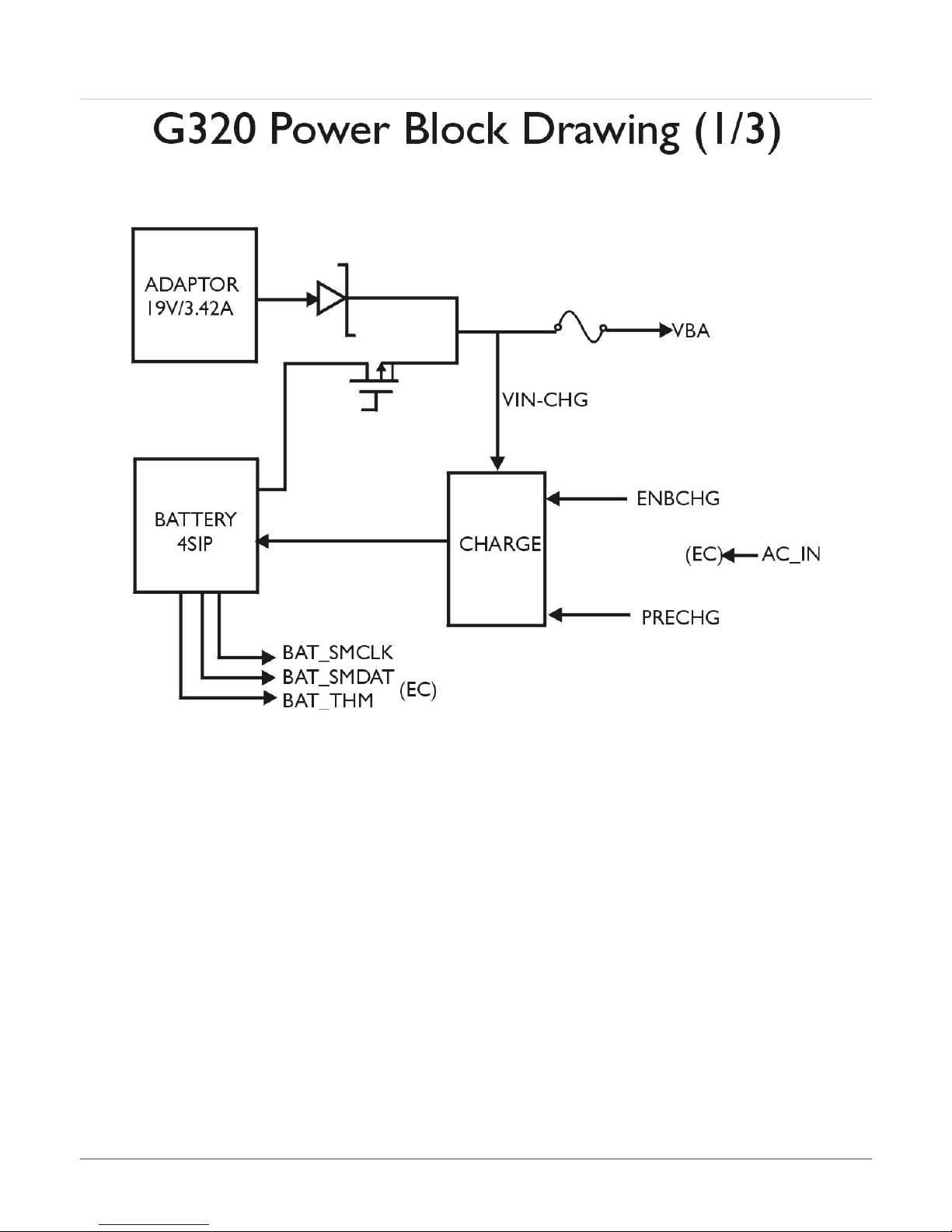
2
Power Supply
11
Page 12
PPoowweerr SSuupppplliieess
G320 can be powered from the following sources:
• Internal, removable, rechargeable LI-ION Battery pack
• International AC adapter (external)
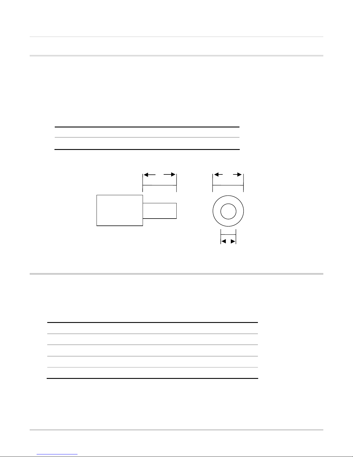
The external power sources connect via the DC-IN port, which has the following characteristics.
Current working range 3.42A
Voltage 19VDC - (8.5V-21.0V)
The adapter is used following connector (all dimensions are millimeters).
Table 9: DC-IN Port characteristics
10 5.5
BBaatttteerryy PPaacckkss
With power management enabled, the LI-ION battery pack gives 1.0 hours typical battery life (at C3 1G / 25 °C) with a TFT screen. The
battery pack has following specification
Capacity 32.56Wh (18650 4 cell 4S1P)
Weight
Charge/Discharge 300cycles(min.)
Remark Smart Battery (SMBUS 1.0)
AC Adapter
The international adapter has a separate AC cable, so that it can be used in different countries by changing the AC cable. The adapter
has the characteristics shown as the following table.
2.5
Table: Main battery pack specification
Li-Ion
260 ± 20 g
12
Page 13

Table : AC Adapter Characteristics(external)
AC cable 6 feet (1.8 meters)
DC cable 5 feet (1.5 meters)
Input 100V to 240VAC, 47 to 63 Hz
Output 19VDC / 3.42A
Size
width
height
length
Weight TBD
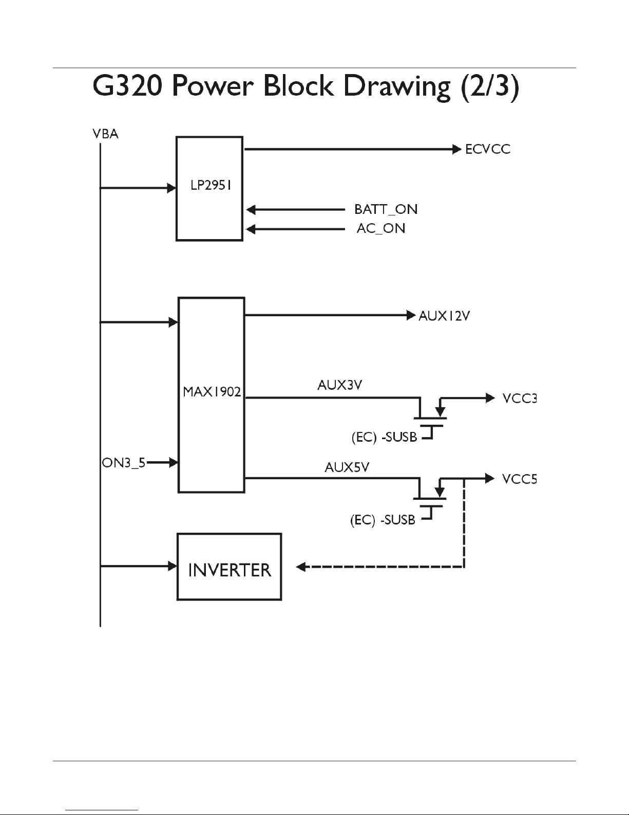
DC/DC POWER Description:
High efficiency, low profile DC/DC converter for notebook computer.
These specifications define the battery charger characteristics and DC/DC converter outputs level.
All of the DC/DC output powers are on the Mother Board system.
Input Characteristics:
Input voltage range: 12.0〜21.0VDC (From AC/DC Adapter or Battery pack )
From adapter: 3.5A max (include charger)
DC/DC Output power description
TYPE SIGNAL DESCRIPTION
1 AUX5V Converter from VBA by buck converter.
TBD
TBD
TBD
Control by signal “ON3_5”.
Provided USB devices power.
Provided INVERTER and periphery device when system turn-on.
2 AUX3V Converter from VBA by buck converter.
Control by signal “ON3_5”.
Provided for remote wake-up function.
Provided for main power when system turn-on..
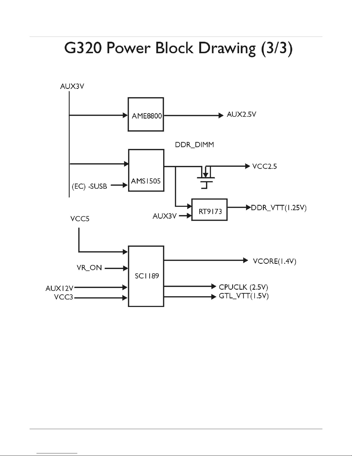
4 VCORE Converter from VCC5 by buck converter
Control by signal “VR_ON”
Provided for CPU CORE/IO power
It can be adjust by signal ‘VID0 – VID4”, and output voltage range is from 1.4V.
5 DDR_DIMM Converter from AUX3V by LDO
Provided DIMM main power when system turn-on.
6 DDR_VTT Converter from VCC_DIMM by LDO. Provided for DDR RAM termination resistor.
13
Page 14

AUX5V
TYPE SIGNAL DESCRIPTION
Converter from VCC_DIMM by LDO Provided.
7 AUX2.5 Converter from AUX3V by LDO
2. Provided for CHIPSET
Scope:
• This voltage is USB devices power supply for wake-up function.
• This voltage is the system’s VCC5 main power (INVERTER/HDD/CD-ROM ..) supply when system is turn on.
• This is a step-down circuit with out of phase technique.
The power supply converts 19.0Vdc from the AC adapter or main battery pack power source to +5Vdc.
•
General characteristics:
Input voltage range Load/Line regulation Ripple
Voltage
12 to 20Vdc +5% ~ -5% 50mV 8.0A 85%
• Over current protection (OCP): Shutdown latch.
• Under Voltage lockout and startup.
• Short circuit protection: Yes. Shutdown latch
• Power on/off sequencing with soft-start.
• Turn on time: 100ms.
• Dynamic response: The voltage keeps 5% regulation when the load changing from 10% to 90%
• Operating temperature: 5°C to 35°C.
• Test condition and instruments:
9 Ripple & Noise: Measuring with bypass capacitors 0.1uf/10uf at output terminal and oscilloscope time-base set at
20MHz. (Tested by the oscilloscope and refer to figure 1)
9 Input voltage set at 12.0V. (DC Power supply)
9 Electronic load: Chroma 63030 or Equivalent
9 Multimeter: FLUKE 87 or Equivalent
9 All measuring refer to figure 2.
Maximum
load current
AUX3V
Efficiency
Scope:
• This voltage is for remove wake-up function.
• This voltage is the system’s VCC3 main power supply when system be turn on..
• This is a step-down circuit with out of phase technique.
• The power supply converts 19Vdc from the AC adapter or Main battery pack power source to +3.3Vdc.
General characteristics:
Input voltage range Load/Line regulation Ripple
14
Voltage
Maximum
load current
Efficiency
Page 15

12 to 20Vdc +5% ~ -5% 50mV 6.0A 85%
• Over current protection (OCP): Shutdown latch.
• Under Voltage lockout and startup.
• Short circuit protection: Yes. Shutdown latch
• Power on/off sequencing with soft-start.
• Turn on time: 100ms.
• Dynamic response: The voltage keeps 5% regulation when the load changing from 10% to 90%
• Operating temperature: 5°C to 35°C.
• Test condition and instruments:
9 Ripple & Noise: Measuring with bypass capacitors 0.1uf/10uf at output terminal and oscilloscope time-base set at
20MHz. (Tested by the oscilloscope and refer to figure 1)
9 Input voltage set at 12.0V. (DC Power supply)
9 Electronic load: Chroma 63030 or Equivalent
9 Multimeter: FLUKE 87 or Equivalent
9 All measuring refer to figure 2.
VCORE
Scope:
• This voltage is for the CPU CORE/CPU IO power.
• The output voltage can be setting from 1.4V by signal “VID0 – VID4”
• This is a step-down circuit output voltage,
General characteristics:
Input voltage range Load/Line regulation Ripple
voltage
5V +2% ~ -2% 10mV 15A 75%
• Over current protection (OCP): Hiccup.
• Short circuit protection: Hiccup.
• Turn on time: 20ms.
• Dynamic response: The voltage keeps 2% regulation when the load changing from 10% to 90%
• Operating temperature: 5°C to 35°C.
• Test condition and instruments:
9 Ripple & Noise: Measuring with by pass capacitors 0.1uf/10uf at output terminal and oscilloscope time-base set at
20MHz. (Tested by the oscilloscope and refer to figure 1)
9 Input voltage set at 5V. (DC Power supply)
9 Electronic load: Chroma 63030 or Equivalent
Maximum
load current
Efficiency
9 Multimeter: FLUKE 87 or Equivalent
9 All measuring refer to figure 2.
AUX2.5V
Scope:
15
Page 16

• Provided for CHIPSET AUX power
• This is a LDO Regulator convert AUX3V to 2.5V.
General characteristics:
Input voltage range Load/Line regulation Ripple voltage Maximum load current
3.3V +5% ~ -5% 50mV 300mA
• Over current protection (OCP): YES.
• Over temperature protection: YES
• Short circuit protection: YES.
• Turn on time: 20ms.
• Dynamic response: The voltage keeps 5% regulation when the load changing from 10% to 90%
• Operating temperature: 5°C to 35°C.
• Test condition and instruments:
9 Ripple & Noise: Measuring with bypass capacitors 0.1uf/10uf at output terminal and oscilloscope time-base set at
20MHz. (Tested by the oscilloscope and refer to figure 1.)
9 Input voltage set at 3.3V. (DC Power supply)
9 Electronic load: Chroma 63030 or Equivalent
9 Multimeter: FLUKE 87 or Equivalent
9 All measuring refer to figure 2.
VCC_DIMM
Scope:
• Provided for DDR_RAM main power when system turn-on
• This is a LDO Regulator convert AUX3.3V to 2.5V.
General characteristics:
Input voltage range Load/Line regulation Ripple Voltage Maximum load current
3.3v +5% ~ -5% 50mV 5A
• Over current protection (OCP): YES.
• Short circuit protection: YES.
• Turn on time: 20ms.
• Dynamic response: The voltage keeps 5% regulation when the load changing from 10% to 90%
• Operating temperature: 5°C to 35°C.
• Test condition and instruments:
9 Ripple & Noise: Measuring with bypass capacitors 0.1uf/10uf at output terminal and oscilloscope time-base set at
20MHz. (Tested by the oscilloscope and refer to figure 1.)
9 Input voltage set at 3.3V. (DC Power supply)
9 Electronic load: Chroma 63030 or Equivalent
9 Multimeter: FLUKE 87 or Equivalent
9 All measuring refer to figure 2.
16
Page 17
DDR_VTT
Scope:
• This voltage is for the DDR DIMM Voltage for termination resistor
• This is convert DDR_DIMM to 1.25V by LDO.
General characteristics:
Input voltage range Load/Line regulation Ripple
voltage
Maximum
load current
Efficiency
2.5V +5% ~ -5% 50mV 1.5 A 50%
• Over current protection (OCP): NO.
• Thermal protect: YES.
• Short circuit protection: YES.
• Turn on time: 100ms.
• Dynamic response: The voltage keeps 5% regulation when the load changing from 10% to 90%
• Operating temperature: 5°C to 35°C.
• Test condition and instruments:
9 Ripple & Noise: Measuring with bypass capacitors 0.1uf/10uf at output terminal and oscilloscope time-base set at
20MHz. (Tested by the oscilloscope and refer to figure 1.)
9 Input voltage set at 2.5V. (DC Power supply)
9 Electronic load: Chroma 63030 or Equivalent
9 Multimeter: FLUKE 87 or Equivalent
9 All measuring refer to figure 2.
+
PROBE
DC
POWER
SUPPLY
GND
0.1U
10U
GND
Figure 1.
A
V
DC/DC
CONVERTER
GND
A
V
ELE.
LOAD
Figure 2.
17
Page 18

BBaatttteerryy CChhaarrggeerr
Scope:
• This is a constant power circuit controlled by using a EC to implement LI-ION Battery charging control.
General characteristics:
• 1 hours to fully charge when system off or in suspend
Charging method:
• Constant -voltage mode and constant-power mode or total power for Li-Ion battery
Charger Cut Off Method for Li-ION Battery:
Current sense:
• When charge mode at CC/CV, and charging current is sensed below 0.1C/cell, then charger cut off.
Li-Ion charge protection:
• Max T: Cut off the charge when the battery temperature exceed 60°C.
• OPT: Operating temperature, check the battery temperature at 0°C to 50°C, then charging the battery.
• Max V: Depend on inside battery pack protection unit spec.
Environment:
Temperature
The G320 temperature specification:
Operating (Non-condensing)
Non-operating (Non-condensing)
Humidity
The G320 humidity specification:
Operating (Non-condensing) 30% ~ 90%RH 10% per hour
Non-operating (Non-condensing) 10% ~ 90%RH 10% per hour
Inverter
General description and features:
The inverter is applied to 14” LCD PANEL notebook computer, and low cost, high performance.
Operating Temperature Range Max. Rate of Change
5° to 35°C 15°C per hour
-20° to 60°C 20°C per hour
Operating Temperature Range Max. Rate of Change
18
Page 19

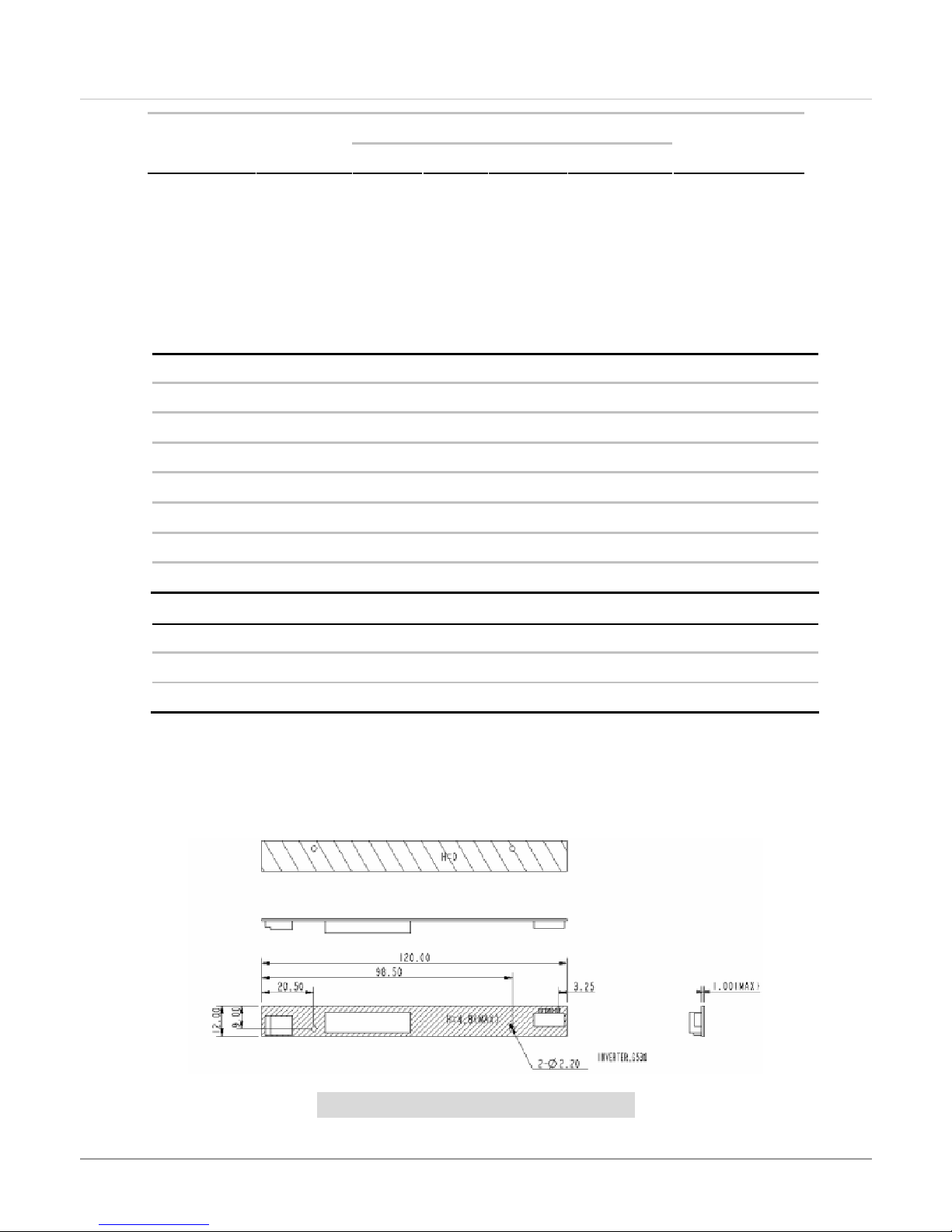
14" LCD PANEL SPEC
Vender DQ DQ
Type DQ141X1LH03 DQ141X11H/2
Min Typ Max Min Typ Max
Lamp Voltage (V) 660 660
Lamp Current (mA) 2.0 4.0 6.0 2.0 4.0 6.0
p Frequency (KHz) 30 60 70 30 60 70
Start Voltage at 0℃ (V)
Start Voltage at 25℃(V)
Power Consumption 2.7 2.7
Connector JST BHSR-02VS-01 JST BHSR-02VS-01
• This inverter’s input voltage is +5V±5% or +19V±5%.
• The inverter can be turned ON /OFF by the signal ‘FPVDDEN‘.
•
The brightness duty can be control by the signal ‘BR_ADJ’.
• The inverter has to follow the following EMI and Safety testing standards.
9 Safety standard: IEC 950, UL1950, CSA 950
9 EMI standard: ANSI C63.4, CISPR 22
1500 1500
1500 1500
Input section:
• Efficiency: 80% (minimum) at full load.
Output section:
Max. output current
ITEM SYMBOL MIN TYP MAX UNIT REMARK
VIN
4.5 5 5.25 V Input voltage
8 21 V
Load is lamp
Input current IIN 780 1000 mArms
Frequency F 48 55 59 KHz
Min. output current
ITEM SYMBOL MIN TYP MAX UNIT REMARK
Input current IIN 340 400 mArms
Frequency F 48 55 59 KHz
5.0 5.5 6.0 mArms Lamp current IL
5.2 5.6 6.0 mArms
4.5 5 5.25 V Input voltage VIN
8 21 V
19
Load is lamp
Page 20
2.0 2.3 2.6 mArms Lamp current IL
The V
lamp must within 100mS
voltage is between 1400V (1500V) and max. output voltage spec of transformer and it must hold over 1 sec. And fully start
OPEN
2.2 2.5 2.8 mArms
Inrush Current
• Make sure fuse can not break at inrush current
Pin Definition & Description
CN1(HRS DF13-7P-1.25H) Pin Definition
PIN SYMBOL COMMENT
1 GND Ground
2 GND Ground
3 LCD Bright Brightness control signal input (0~3.3)
4 Enable Voltage 5Vdc Input
5 Vin 5Vdc Input
6 Vin 5Vdc Input
7 Main Power DC Input 8V~21V
CN2(JST SM02B-BHSS-1-TB) Pin Definition
PIN SYMBOL DESCRIPTION
1 AC+ Positive CCFL terminal
2 AC- Negative CCFL terminal
Protection:
• SCP (Short Circuit Protection): There is no damage when short H.V. to GND.
• Open Lamp Protection: There is no damage when H.V. is open
Dimension:
Input screw hole add a circle pad, pad wide=1mm.
20
Page 21

Burn-in Testing
Environment:
• Burn-in condition:
9 Ambient Temperature: 35 – 45 °C
9 Percentage of Load : Full Load
• Burn-in Time:
9 Initial Burn-in Time is 24Hr.
9 If the failure rate is less than 1%, then the Burn-in time can be changed to 4Hr.
Item Range Condition Remark
0 – 45 °C
Operation
Temperature
-20 – 60 °C
Storage
10 – 90 % Operation
Humidity
5 – 95 % Storage Noncondensing
Other:
• Add a resistor 0 ohm between GND and PTH HOLE.
• Add a no masked area of GND PLANE on solder side, under CN1 connector.
• The input voltage can not cross talk when use dimming control
21
Page 22
22
Page 23
23
Page 24
24
Page 25

3
DMA,
Timer/Counter
25
Page 26

DDMMAA CChhaannnneell
DMA Channel Number Function
Channel 0 Available
Channel 1 Available
Channel 2 Floppy disk
Channel 3 ECP Support
Channel 4 [ Cascade ]
Channel 5 Available
Channel 6 Available
Channel 7 Available
PPrrooggrraammmmaabbllee TTiimmeerr//CCoouunntteerrss
Channel Number Function
Channel 0 Supports system timer
Channel 1 Supports refresh cycles
Channel 2 Supports the audio speaker
26
Page 27

4
Interrupts
27
Page 28

IInntteerrrruupptt
Interrupt Function
IRQ 0 System Timer
IRQ 1 Keyboard
IRQ 2 Cascade from PIC
IRQ 3 Available
IRQ 4 COM1
IRQ 5 Reserved
IRQ 6 FDC
IRQ 7 LPT 1
IRQ 8 Clock/Calendar
IRQ 9 ACPI SCI IRQ
IRQ 10 USB/LAN/VGA
IRQ 11 Audio/Modem
IRQ 12 Touch pad
IRQ 13 Coprocessor
IRQ 14 Fixed disk controller
IRQ 15 IDE CD-ROM
28
Page 29

5
Memory Address
Mapping
29
Page 30

MMeemmoorryy AAddddrreessss MMaappppiinngg
30
Page 31

6
I/O Address
Mapping
31
Page 32

II//OO AAddddrreessss MMaappppiinngg
Hexadecimal Range Devices Usage
00-01F Master DMA Controller System
20-03F Master interrupt controller System
40-05F Timer/Counter System
60,064 Keyboard controller System
(60h) KBC data System
(61h) System speaker System
(64h) KBC command/status System
70-77 RTC/CMOS/NMI-disable System
78-7F -available for system use- System
80 -reserved- (debug port) System
81-8F DMA page registers System
90-91 -available for system use- System
92 System control System
93-9F -available for system use- System
A0-BF Slave interrupt controller System
C0-DF Slave DMA controller System
E0-FF -available for system use- System
100-CF7 -available for system use* System
CF8-CFB PCI configuration address System
CFC-CFF PCI configuration data System
D00-FFFF -available for system use- System
378-37F Parallel port (standard & EPP) I/O
3F0-3F1 Configuration index/data I/O
3F0-3F7 Floppy controller I/O
778-77A Parallel port (ECP extensions) (port 378+400) I/O
32
Page 33

Connector and Pin
Assignment
7
33
Page 34

TThhee PPiinn AAssssiiggnnmmeenntt ooff VViiddeeoo PPoorrtt
Pin Signal Pin Signal
1 Red 9 NC
2 Green 10 Ground
3 Blue 11 MSO
4 NC 12 MS1
5 Ground 13 Horizontal Sync
6 Ground 14 Vertical Sync
7 Ground 15 NC
8 Ground
TThhee PPiinn AAssssiiggnnmmeenntt ooff PPaarraalllleell PPoorrtt
Pin Signal Pin Signal
1 -STROBE 14 -AUTO FEED
2 D0 15 -ERROR
3 D1 16 -INIT
4 D2 17 -SLCT IN
5 D3 18 GND
6 D4 19 GND
7 D5 20 GND
8 D6 21 GND
9 D7 22 GND
10 -ACK 23 GND
11 BUSY 24 GND
34
Page 35

Pin Signal Pin Signal
12 PE 25 GND
13 SLCT
35
Page 36

36
Page 37

8
INT Function
37
Page 38

The following lists the available interrupt services made through the system BIOS. For detailed information about each function,
refer to any one of the many books on interrupts.
INT Type Function
02 Logical Non-maskable Interrupt
05h Software Print Screen
08h Hardware System Timer
09h Hardware Keyboard
0Ah Hardware Slave PIC Redirect
0Eh Hardware Diskette
10h Software Video
AH Value Function
00h Set video mode
01h Set cursor type
02h Set cursor position
03h Read current cursor position
04h Not supported
05h Select new video page
06h Scroll current page up
07h Scroll current page down
08h Read character/Attribute to screen
09h Write character/attribute from screen
0Ah Write character only to screen
0Bh Set color palette
0Ch Write pixel
0Dh Read pixel
0Eh Write teletype to active page
0Fh Return video status
10h-12h not supported
13h Write String
14h-ffh reserved
11h Software Equipment List
12h Software Memory Size
13h Software Diskette Service (Interrupt 40h)
AH Value Function
00h Reset diskette system
38
Page 39

01h Read diskette status
02h Read diskette sectors
03h Write diskette sectors
04h Verify diskette sectors
05h Format diskette track
06h,07h Reserved
08h Read drive parameters
09h-14h reserved
15h Read drive type
16h Detect media change
17h Set diskette type
18h Set media type for format
19h-FFh reserved
13h Software Hard disk services
AH Value Function
00h Reset disk system
01h Read disk status
02h Read disk sectors
03h Write disk sectors
04h Verify disk sectors
05h Format disk cylinder
06h,07h Reserved
08h Read drive parameters
09h Initialize drive parameters
0Ah Read long disk sectors
0Bh write long disk sectors
0Ch Seek to cylinder
0Dh Alternate reset fixed disk
0Eh Diagnostics 1, read test buffer
0Fh Diagnostics 2, write test buffer`
10h Test for drive ready
11h Recalibrate drive
12h-14h reserved
15h Read disk type
16h-18h reserved
39
Page 40

19h, 1Ah Not supported
1Bh-FFh Reserved
14h Software Serial Communication
AH Value Function
00h Initialize serial communication port
01h Send character
02h Receive character
03h Read serial port status
04h-FFh reserved
15h Software System Services
AH Value Function
00h-4Eh reserved
4Fh Keyboard intercept
50h-7Fh reserved
80h Device open
81h Device close
82h Program termination
83h Set event wait interval
84h Joystick support
85h System request key
86h Wait
87h Move block
88h Read extended memory size
89h Switch processor to protected mode
8Ah-8Fh Reserved
90h Device busy loop
91h Interrupt complete
92h-BFh Reserved
C0h Return system configuration parameters
C1h Return extended BIOS data area segment address
C2h Pointing device interface
C3h-FFh Reserved
16h Software Keyboard
AH Value Function
00h Read keyboard input
40
Page 41

01h Return keyboard status
02h Return shift flag status
03h Set typematic rate and delay
04h Reserved
05h Store key data
06h-0Fh reserved
10h Read extended key input
11h Return extended keyboard status
12h Return extended shift flags status
13h-FFh reserved
17h Software Parallel Printer
AH Value Function
00h Print character
01h Initialize printer
02h Read printer status
03h-FFh reserved
18h Software Load ROM BASIC
19h Software Bootstrap Loader
1Ah Software System Timer and Real-Time Clock
AH Value Function
00h Read system timer time counter
01h Set system timer time counter
02h Read real time clock time
03h Set real time clock time
04h Read real time clock date
05h Set real time clock date
06h Reserved
07h Set real time clock alarm
08h Read day of week from real time clock(SystmeSoft only)
09h Write day of week to real time clock(SystemSoft only)
0Ah-FFh Reserved
1Bh Software Keyboard Break
1Ch User User timer tick
1Dh BIOS table Video parameters table
1Eh BIOS table Diskette parameters table
41
Page 42

1Fh User Video graphics characters
40h Software diskette BIOS receptor
41h BIOS table Fixed disk parameter table
46h BIOS table Fixed disk parameter table
70h Hardware Real time clock
71h Hardware Redirect cascade
74h Hardware Pointing device(Mouse)
76h Hardware fixed disk
Any 80386 and/or coprocessor exception interrupts normally handled by the operating system are vectored by default to the BIOS
at system power-on.
42
Page 43

9
BIOS Setup
43
Page 44

44
Page 45

45
Page 46

46
Page 47

Post Code & Error
Handling
10
47
Page 48

AAMMIIBBIIOOSS EErrrroorr MMeessssaaggeess aanndd BBeeeepp CCooddeess
Beep Codes
Errors can occur during POST (Power On Self Test), which is performed every time the computer is powered on. Fatal errors (see
below) are communicated through a series of audible beeps. All errors except Beep Code 8 are fatal errors. Fatal errors do not
allow the computer to continue the boot process. Most displayed errors allow the computer to continue the boot process.
Beeps Error message Description
1 Refresh Failure The memory refresh circuitry on the motherboard is faulty.
2 Parity Error Parity error in the first 64 KB of memory.
3 Base 64 KB Memory
Failure
4 Timer Not Operational Memory failure in the first 64 KB of memory, or Timer 1 on the motherboard is not
5 Processor Error The CPU (Central Processing Unit) on the motherboard generated an error.
6 8042 – Gate A20 Failure The keyboard controller (8042) may be bad. The BIOS cannot switch to protected
7 Processor Exception
Interrupt Error
Memory failure in first 64 KB.
functioning.
mode.
The CPU generated an exception interrupt.
8 Display Memory
Read/Write Error
9 ROM Checksum Error The ROM checksum value does not match the value encoded in the BIOS.
10 CMOS Shutdown Register
Read/Write Error
11 Cache Error/
External Cache Bad
Displayed Fatal Error Messages
The computer halts after the following messages and cannot be rebooted until a physical change is made.
• CMOS not operational
• 8042-Gate A20 error
• DMA error
• DMA #1 error
• DMA #2 error
• FDD Controller failure
• HDD Controller failure
• INTR #1 error
• INTR #2 error
• On Board parity error
• On Board Parity error
The system video adapter is either missing or its memory is faulty. This is not a fatal
error.
The shutdown register for CMOS RAM failed.
The external cache is faulty.
48
Page 49

AMIBIOS POST Error Message Format
• ERROR Message Line 1
• ERROR Message Line 2
• Press <F1> to RESUME
The <F1> prompt message is not displayed if
error messages, there is only one message. If a second message appears, it is Run Setup
Press <F1> to run AMIBIOS Setup.
Error Message Explanation
8042 Gate – A20 Error Gate A20 on the keyboard controller (8042) is not working. Replace the 8042.
Address Line Short! Error in the address decoding circuitry on the motherboard.
C: Drive Error Hard disk drive C: does not respond. Run AMIDiag to correct this problem. Also, check the C: hard
disk type in Standard Setup to make sure that the hard disk drive type is correct.
C: Drive Failure Hard disk drive C: does not respond. Replace the hard disk drive.
Cache Memory Bad, Do Not
Enable Cache!
CH-2 Timer Error Most ISA computers include two timers. There is an error in timer 2.
CMOS Battery State Low CMOS RAM is powered by a battery. The battery power is low. Replace the battery.
CMOS Checksum Failure After CMOS RAM values are saved, a checksum value is generated for error checking. The
CMOS System Options Not
Set
Cache memory is defective. Replace it.
previous value is different from the current value. Run AMIBIOS Setup.
The values stored in CMOS RAM are either corrupt or nonexistent. Run AMIBIOS Setup.
Wait for <F1> If Any Error
in Advanced Setup has been set to
Disabled.
For most displayed
CMOS Display Type
Mismatch
CMOS Memory Size
Mismatch
CMOS Time and Date Not
Set
D: Drive Error Hard disk drive D: does not respond. Run AMIDiag. Also check the D: hard disk type in Standard
D: drive failure Hard disk drive D: does not respond. Replace the hard disk drive.
Diskette Boot Failure The boot disk in floppy drive A: is corrupt. It cannot be used to boot the computer. Use another
Display Switch Not Proper Some computers require a video switch on the motherboard be set to either color or
DMA Error Error in the DMA controller.
DMA #1 Error Error in the first DMA channel.
DMA #2 Error Error in the second DMA channel.
The video type in CMOS RAM does not match the type detected by the BIOS. Run AMIBIOS Setup.
The amount of memory on the motherboard is different than the amount in CMOS RAM. Run
AMIBIOS Setup.
Run Standard Setup to set the date and time.
Setup to make sure that the hard disk drive type is correct.
boot disk and follow the screen instructions.
monochrome. Turn the computer off, set the switch, then power on.
49
Page 50

FDD Controller Failure The BIOS cannot communicate with the floppy disk drive controller. Check all appropriate
connections after the computer is powered down.
HDD Controller Failure The BIOS cannot communicate with the hard disk drive controller. Check all appropriate
connections after the computer is powered down.
INTR #1 Error Interrupt channel 1 failed POST.
INTR #2 Error Interrupt channel 2 failed POST.
Invalid Boot Diskette The BIOS can read the disk in floppy drive A:, but cannot boot the computer. Use another boot disk.
Keyboard Is
Locked...Unlock It
Keyboard Error Keyboard timing problem. Set the Keyboard option in Standard Setup to Not Installed to skip the
KB/Interface Error There is an error in the keyboard connector.
No ROM BASIC Cannot find a bootable sector on either disk drive A: or hard disk drive C:. The BIOS calls INT 18h
Off Board Parity Error Parity error in memory installed in an expansion slot. The format is:
On Board Parity Error Parity error in motherboard memory. The format is:
Parity Error ???? Parity error in system memory at an unknown address. Run AMIDiag to find and correct memory
The keyboard lock on the computer is engaged. The computer must be unlocked to continue.
keyboard POST routines.
which generates this message. Use a bootable disk.
OFF BOARD PARITY ERROR ADDR (HEX) = (XXXX)
XXXX is the hex address where the error occurred. Run AMIDiag to find and correct memory
problems.
ON BOARD PARITY ERROR ADDR (HEX) = (XXXX)
XXXX is the hex address where the error occurred. Run AMIDiag to find and correct memory
problems.
problems.
POST Checkpoint Codes
POST is performed by the BIOS when the computer is reset or rebooted. POST tests and initializes key components. When a POST
routine completes, a code is written to I/O port address 80h. Display this code by attaching diagnostic equipment to I/O port
address 0080h. The following POST checkpoint codes are valid for all AMIBIOS with a core BIOS date of 7/15/95 and a version
number of 6.14 or later.
Uncompressed Initialization Codes The uncompressed initialization checkpoint codes (in order of execution) are:
Code Description
D0h The NMI is disabled. Power on delay is starting. Next, the initialization code checksum will be verified.
D1h Initializing the DMA controller, performing the keyboard controller BAT test, starting memory refresh, and entering 4
GB flat mode next.
D3h Starting memory sizing next.
D4h Returning to real mode. Executing any OEM patches and setting the stack next.
D5h Passing control to the uncompressed code in shadow RAM at E000:0000h.The initialization code is copied to segment
0 and control will be transferred to segment 0.
50
Page 51

Code Description
D6h Control is in segment 0. Next, checking if <Ctrl> <Home> was pressed and verifying the system BIOS checksum. If
either <Ctrl> <Home> was pressed or the system BIOS checksum is bad, next will go to checkpoint code E0h.
Otherwise, going to checkpoint code D7h.
D7h Passing control to the interface module next.
D8h The main system BIOS runtime code will be decompressed next.
D9h Passing control to the main system BIOS in shadow RAM next.
Bootblock Recovery Codes The bootblock recovery checkpoint codes are (in order of execution):
Code Description
E0h The onboard floppy controller if available is initialized. Next, beginning the base 512 KB memory test.
E1h Initializing the interrupt vector table next.
E2h Initializing the DMA and Interrupt controllers next.
E6h Enabling the floppy drive controller and Timer IRQs. Enabling internal cache memory.
EDh Initializing the floppy drive.
EEh Looking for a floppy diskette in drive A:. Reading the first sector of the diskette.
EFh A read error occurred while reading the floppy drive in drive A:.
F0h Next, searching for the AMIBOOT.ROM file in the root directory.
F1h The AMIBOOT.ROM file is not in the root directory.
F2h Next, reading and analyzing the floppy diskette FAT to find the clusters occupied by the AMIBOOT.ROM file.
F3h Next, reading the AMIBOOT.ROM file, cluster by cluster.
F4h The AMIBOOT.ROM file is not the correct size.
F5h Next, disabling internal cache memory.
FBh Next, detecting the type of flash ROM.
FCh Next, erasing the flash ROM.
FDh Next, programming the flash ROM.
FFh Flash ROM programming was successful. Next, restarting the system BIOS.
Uncompressed Initialization Codes The following runtime checkpoint codes are in order of execution. These codes are
uncompressed in F0000h shadow RAM.
Code Description
03h The NMI is disabled. Next, checking for a soft reset or a power on condition.
05h The BIOS stack has been built. Next, disabling cache memory.
06h Uncompressing the POST code next.
07h Next, initializing the CPU and the CPU data area.
08h The CMOS checksum calculation is done next.
0Bh Next, performing any required initialization before the keyboard BAT command is issued.
51
Page 52

Code Description
0Ch The keyboard controller input buffer is free. Next, issuing the BAT command to the keyboard controller.
0Eh The keyboard controller BAT command result has been verified. Next, performing any necessary initialization after
the keyboard controller BAT command test.
0Fh The initialization after the keyboard controller BAT command test is done. The keyboard command byte is written
next.
10h The keyboard controller command byte is written. Next, issuing the Pin 23 and 24 blocking and unblocking commands.
11h Next, checking if the <End or <Ins> keys were pressed during power on. Initializing CMOS RAM if the
RAM in every boot
AMIBIOS POST option was set in AMIBCP or the <End> key was pressed.
Initialize CMOS
12h Next, disabling DMA controllers 1 and 2 and interrupt controllers 1 and 2.
13h The video display has been disabled. Port B has been initialized. Next, initializing the chipset.
14h The 8254 timer test will begin next.
19h The 8254 timer test is over. Starting the memory refresh test next.
1Ah The memory refresh line is toggling. Checking the 15 second on/off time next.
23h Reading the 8042 input port and disabling the MEGAKEY Green PC feature next. Making the BIOS code segment
writable and performing any necessary configuration before initializing the interrupt vectors.
24h The configuration required before interrupt vector initialization has completed. Interrupt vector initialization is about
to begin.
25h Interrupt vector initialization is done. Clearing the password if the POST DIAG switch is on.
27h Any initialization before setting video mode will be done next.
28h Initialization before setting the video mode is complete. Configuring the monochrome mode and color mode settings
next.
2Ah Bus initialization system, static, output devices will be done next, if present.
2Bh Passing control to the video ROM to perform any required configuration before the video ROM test.
2Ch All necessary processing before passing control to the video ROM is done. Looking for the video ROM next and passing
control to it.
2Dh The video ROM has returned control to BIOS POST. Performing any required processing after the video ROM had
control.
2Eh Completed post-video ROM test processing. If the EGA/VGA controller is not found, performing the display memory
read/write test next.
2Fh The EGA/VGA controller was not found. The display memory read/write test is about to begin.
30h The display memory read/write test passed. Look for retrace checking next.
31h The display memory read/write test or retrace checking failed. Performing the alternate display memory read/write
test next.
32h The alternate display memory read/write test passed. Looking for alternate display retrace checking next.
34h Video display checking is over. Setting the display mode next.
37h The display mode is set. Displaying the power on message next.
38h Initializing the bus input, IPL, and general devices next, if present.
52
Page 53

Code Description
39h Displaying bus initialization error messages.
3Ah The new cursor position has been read and saved. Displaying the
Hit <DEL>
message next.
40h Preparing the descriptor tables next.
42h The descriptor tables are prepared. Entering protected mode for the memory test next.
43h Entered protected mode. Enabling interrupts for diagnostics mode next.
44h Interrupts enabled if the diagnostics switch is on. Initializing data to check memory wraparound at 0:0 next.
45h Data initialized. Checking for memory wraparound at 0:0 and finding the total system memory size next.
46h The memory wraparound test has completed. The memory size calculation has been completed. Writing patterns to
test memory next.
47h The memory pattern has been written to extended memory. Writing patterns to the base 640 KB memory next.
48h Patterns written in base memory. Determining the amount of memory below 1 MB next.
49h The amount of memory below 1 MB has been found and verified. Determining the amount of memory above 1 MB
memory next.
4Bh The amount of memory above 1 MB has been found and verified. Checking for a soft reset and clearing the memory
below 1 MB for the soft reset next. If this is a power on situation, going to checkpoint 4Eh next.
4Ch The memory below 1 MB has been cleared via a soft reset. Clearing the memory above 1 MB next.
4Dh The memory above 1 MB has been cleared via a soft reset. Saving the memory size next. Going to checkpoint 52h next.
4Eh The memory test started, but not as the result of a soft reset. Displaying the first 64 KB memory size next.
4Fh The memory size display has started. The display is updated during the memory test. Performing the sequential and
random memory test next.
50h The memory below 1 MB has been tested and initialized. Adjusting the displayed memory size for relocation and
shadowing next.
51h The memory size display was adjusted for relocation and shadowing. Testing the memory above 1 MB next.
52h The memory above 1 MB has been tested and initialized. Saving the memory size information next.
53h The memory size information and the CPU registers are saved. Entering real mode next.
54h Shutdown was successful. The CPU is in real mode. Disabling the Gate A20 line, parity, and the NMI next.
57h The A20 address line, parity, and the NMI are disabled. Adjusting the memory size depending on relocation and
shadowing next.
58h The memory size was adjusted for relocation and shadowing. Clearing the
59h The
Hit <DEL>
message is cleared. The
<WAIT...>
message is displayed. Starting the DMA and interrupt controller test
Hit <DEL>
message next.
next.
60h The DMA page register test passed. Performing the DMA Controller 1 base register test next.
62h The DMA controller 1 base register test passed. Performing the DMA controller 2 base register test next.
65h The DMA controller 2 base register test passed. Programming DMA controllers 1 and 2 next.
66h Completed programming DMA controllers 1 and 2. Initializing the 8259 interrupt controller next.
7Fh Extended NMI source enabling is in progress.
53
Page 54

Code Description
80h The keyboard test has started. Clearing the output buffer and checking for stuck keys. Issuing the keyboard reset
command next.
81h A keyboard reset error or stuck key was found. Issuing the keyboard controller interface test command next.
82h The keyboard controller interface test completed. Writing the command byte and initializing the circular buffer next.
83h The command byte was written and global data initialization has completed. Checking for a locked key next.
84h Locked key checking is over. Checking for a memory size mismatch with CMOS RAM data next.
85h The memory size check is done. Displaying a soft error and checking for a password or bypassing WINBIOS Setup
next.
86h The password was checked. Performing any required programming before WINBIOS Setup next.
87h The programming before WINBIOS Setup has completed. Uncompressing the WINBIOS Setup code and executing the
AMIBIOS Setup or WINBIOS Setup utility next.
88h Returned from WINBIOS Setup and cleared the screen. Performing any necessary programming after WINBIOS Setup
next.
89h The programming after WINBIOS Setup has completed. Displaying the power on screen message next.
8Bh The first screen message has been displayed. The
<WAIT...>
message is displayed. Performing the PS/2 mouse check
and extended BIOS data area allocation check next.
8Ch Programming the WINBIOS Setup options next.
8Dh The WINBIOS Setup options are programmed. Resetting the hard disk controller next.
8Fh The hard disk controller has been reset. Configuring the floppy drive controller next.
91h The floppy drive controller has been configured. Configuring the hard disk drive controller next.
95h Initializing the bus option ROMs from C800 next.
96h Initializing before passing control to the option ROM at C800.
97h Initialization before the C800 option ROM gains control has completed. The option ROM check is next.
98h The option ROM had control and has now returned control to BIOS POST. Performing any required processing after
the option ROM returned control.
99h Any initialization required after the option ROM test has completed. Configuring the timer data area and printer base
address next.
9Ah Set the timer and printer base addresses. Setting the RS-232 base address next.
9Bh Returned after setting the RS-232 base address. Performing any required initialization before the Coprocessor test
next.
9Ch Required initialization before the Coprocessor test is over. Initializing the Coprocessor next.
9Dh Coprocessor initialized. Performing any required initialization after the Coprocessor test next.
9Eh Initialization after the Coprocessor test is complete. Checking the extended keyboard, keyboard ID, and Num Lock key
next. Issuing the keyboard ID command next.
A2h Displaying any soft errors next.
A3h The soft error display has completed. Setting the keyboard typematic rate next.
54
Page 55

Code Description
A4h The keyboard typematic rate is set. Programming the memory wait states next.
A5h Memory wait state programming is over. Clearing the screen and enabling parity and the NMI next.
A7h NMI and parity enabled. Performing any initialization required before passing control to the option ROM at E000 next.
A8h Initialization before passing control to the option ROM at E000h completed. Passing control to the option ROM at
E000h next.
A9h Returned from option ROM at E000h control. Performing any initialization required after the E000 option ROM had
control next.
AAh Initialization after E000 option ROM control has completed. Displaying the system configuration next.
ABh Building the multiprocessor table, if necessary.
ACh Uncompressing the DMI data and initializing DMI POST next.
B0h The system configuration is displayed.
B1h Copying any code to specific areas.
00h Code copying to specific areas is done. Passing control to INT 19h boot loader next.
Bus Checkpoint Codes The system BIOS passes control to buses at:
Code Description
2Ah Initializing the different bus system, static, and output devices, if present.
38h Initialized bus input, IPL, and general devices, if present.
39h Displaying bus initialization error messages, if any.
95h Initializing bus option ROMs from C8000h through D8000h.
55
Page 56

11
Replacing the
Battery
56
Page 57

IInnsseerrttiinngg aanndd RReemmoovviinngg tthhee BBaatttteerryy PPaacckk
The battery pack should already be inserted in your Notebook computer when you unpack it. If not inserted, follow these directions:
1.
Turn over the notebook and place it on a solid, flat surface.
2.
Angle the battery into the bay. The front edge of the battery should slide into the grooves in the system case.
Gently lower the battery into the bay and push it until it clicks securely in the bay.
To remove the battery pack:
1. Turn off the notebook, and disconnect the AC adapter. Close the LCD panel and turn it
over and place it on a solid, flat surface.
2. Lift the release latch to release the battery from the bay. At this time the battery will now
be angled slightly out of the bay.
3. Hold the battery at the finger grip and lift it out of the compartment.
57
Page 58

12
Upgrading your
System
58
Page 59

Upgrading your Memory
Refer to the following instructions and illustration for information on upgrading your notebook's memory.
1.
Turn off the computer and disconnect the AC adapter and all peripherals.
2.
Turn the notebook over so that the rear ports are facing you and locate the memory module compartment.
3.
Remove the screws that secure the RAM module compartment cover and set it aside in a safe place.
4.
Remove the compartment cover and then angling it up and out.
5.
If you need to install a higher capacity module, gently push the edge clips on both sides to release the module.
Angle the card slightly upward and gently slide it from its edge connector slot. Store the card in the anti-static
bag that contains your new module(s).
6.
To install the new memory card, hold the card with its gold edge connector toward the edge connector slot of the
compartment. To help you orient the cards, the edge connector has been made with two unequal-length sections.
You will only be able to insert the card in one direction.
59
Page 60

7.
Insert the edge connector into the slot. The gold edge connector of the card should not be visible when the card
is fully inserted.
8.
Press the card downward where you should hear an audible click as the latches of the connector secure the card
in place.
9.
Once the module is properly seated, you can replace the cover on this compartment.
10.
Replace and tighten the screw.
Easy to Upgrade HDD Module
The hard drive in your notebook computer is made to be easily swapped out for upgrading. You should back up your hard drive
before attempting o change the hard drive.
Make sure that before you install a new drive, all the files in your system should be backed up.
How to upgrade your Hard Drive
1.
Power down the system completely. Turn the system over with the front of the unit facing you.
2.
Remove the two screws that secure the compartment cover and set them in a safe place.
3.
Slide the HDD cover away from the compartment.
4.
The drive is attached to a special bracket that secures it to the notebook computer. There are 2 screws that
hold the bracket.
5.
Push the HDD slightly as shown in the illustration to release it from the pins of the drive.
6.
Gently hold the grip of the HDD, lift it up to release from its compartment.
60
Page 61

7.
To install the new HDD, you will need to align the tabs on the drive bracket with the slots on the bay. Press down
gently on the drive bracket until it engages with the system. Do not force the drive into place this can bend the
pins on the hard drive.
8.
Slide the compartment cover into place and be sure the screw holes on the cover align completely with the
screw holes in the case.
9.
Secure the cover with the two screws.
61
Page 62

Page 63

13
Jumper Setting
63
Page 64

JJuummppeerr SSeettttiinngg
FUNCTION
LOCATION
3 Normal Use Programming uP from ICE
4 Normal Use Programming uP from ICE
1 2
ON ON QDI 14.1” XGA TFT
ON OFF Reserved
OFF ON Reserved
OFF OFF Reserved
ON Off
Panel Type
64
Page 65

14
Schematic
65
Page 66

66
Page 67

15
System Block
Diagram
67
Page 68

68
Page 69

16
Main Board
Layout
Placement
69
Page 70

70
Page 71

17
System &
Modular Parts
Assembly and
Disassembly
Diagram
71
Page 72

72
Page 73

73
Page 74

74
Page 75

75
Page 76

76
Page 77

77
Page 78

78
Page 79

79
Page 80

80
Page 81

81
Page 82

82
Page 83

83
Page 84

84
Page 85

85
 Loading...