

Page 1

AT2550
Wolverine
2.5” IDE Solid State Flash Drive
User Guide
153999-001
Revision 3.2
December 8, 2003
Memtech SSD Corporation
7628 Las Positas Road
Livermore, CA 94550
(925) 294-8483
(800) 445-5511
www.memtech.com
Page 2

Table of Contents
1. HIGHLIGHTS ...............................................................................3
2. INTRODUCTION..........................................................................3
3. INSTALLATION ...........................................................................4
3.1 PROCEDURE ...........................................................................................................4
3.2 JUMPERS................................................................................................................6
3.3 IDE INTERFACE.....................................................................................................10
4. OPERATION ..............................................................................12
4.1 ACTIVE REMAP™ AND WRITE LIMITATIONS .............................................................. 12
4.2 ECC ...................................................................................................................... 12
4.3 POWER ................................................................................................................ 13
4.4 TROUBLE SHOOTING GUIDE .................................................................................... 14
5. MAINTENANCE.........................................................................14
6. SPECIFICATIONS .....................................................................15
6.1 INTERFACE ........................................................................................................... 15
6.2 PERFORMANCE .....................................................................................................15
6.3 ENVIRONMENTAL................................................................................................... 15
6.4 POWER REQUIREMENTS ........................................................................................15
6.5 MECHANICAL.........................................................................................................16
6.6 RELIABILITY ..........................................................................................................16
7. APPENDIX .................................................................................17
7.1 CONTACT INFORMATION .........................................................................................17
7.2 ATA SPECIFICATION INFORMATION ......................................................................... 17
7.3 LIMITED LIFETIME WARRANTY ................................................................................17
AT2550 User Guide December 8, 2003 page 2 of 17
Page 3

1. HIGHLIGHTS
• 4.8 Gbyte capacity under 9.5mm
• 8.7 Gbyte capacity under 12.5mm
• 27 Gbyte maximum capacity
• Full -55
o
C to +125oC military temperature range
• 5 volt, low power operation
• Completely solid state - no moving parts and no batteries
• Extremely Rugged - 1000G operating shock, 15G operating vibration
• 2.5” drive form factor with a 44 pin, 2mm IDE interface
• 16-byte CRC/ECC and Active Remap™ for exceptional data reliability
• UDMA-66 compliant ATA interface
• 0.1 millisecond access time
• 26 Mbyte/second cached read throughput
• 20 Mbyte/second cached write throughput
• 16 Mbyte SDRAM buffer
• Nonvolatile NAND E
2
PROM with 10 year data retention
• EMC and CSA Safety Compliant
2. INTRODUCTION
The AT2550 “Wolverine” is a new line of IDE solid state drives available in a lowprofile 2.5-inch format. The drive is completely solid state, making it exceptionally
rugged and able to operate in extreme environmental conditions.
Sector Erasable NAND E
2
PROM (Flash) is used to provide up to 27 Gbytes of
nonvolatile, solid state storage in an extremely small, rugged form factor. The
drive is 100% IDE compatible and requires no special drivers to operate. It is
essentially a drop in replacement for standard rotating media.
The IDE interface is implemented using a commercially available IDE controller. It
supports UDMA-66 transfers, LBA mode addressing, and incorporates a 1 Mbyte
buffer, and a 16-byte hardware error detection and correction logic. The
CRC/ECC circuitry, in conjunction with Memtech’s proprietary Active Remap™
technology, makes for a virtually bulletproof medium for data retention.
The drive can be operated in both caching and non-caching modes, and is
configured via the operating system. When caching is enabled, the full 16 Mbyte
SDRAM buffer is available as a direct mapped cache. When used in the noncaching mode, a small portion buffer is employed, and all new data is committed
to flash before a write routine is completed.
The drive is available in a number of standard capacities ranging from 1 Gbyte to
27 Gbytes. Drives under 4.8 Gbytes are 9.5mm tall, while 8.7 Gbyte capacity
drives are 12.5mm tall.
Each drive is fully tested under environmental extremes at the factory using
Memtech’s proprietary EnduroTest™ to guarantee data integrity in even the
harshest conditions. Full functionality of the product is guaranteed out of the box.
AT2550 User Guide December 8, 2003 page 3 of 17
Page 4
3. INSTALLATION
3.1 PROCEDURE
3.1.1 ESD PRECAUTIONS
The AT2550 is sensitive to static electricity. Before handling the AT2550, please
observe the following precautions to avoid ESD damage to the unit:
• Keep the drive in its shielded bag until ready to install.
• Ground yourself by touching a grounded chassis frame of the computer, or
use a grounded wrist strap before and during the installation process.
• Do not touch the exposed drive electronics or connectors. Always handle the
drive by the edges or mounting rails.
3.1.2 CONFIGURATION
Before applying power to the drive, configure the drive using the jumper diagrams
given in Section 3.2. The default configuration is for a single drive system or as
the master in a two-drive system. Change the configuration as required. Never
attempt to change the jumpers while the drive is plugged in and the computer is
on.
3.1.3 CABLE
With the computer off, attach the 44-pin 2mm cable connector to the 2mm
connector on the drive. Note pin 1 orientation and alignment. Care should be
taken when installing the cable, as misalignment can permanently damage the
drive interface. No power cable is required as the 2mm ribbon cable connector
supplies power to the drive.
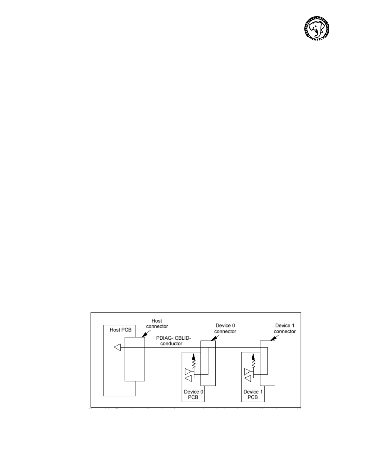
The AT2550 is UDMA66 compliant with the appropriate cable. If the host system
does not detect the correct cable type, the interface will restrict transfers to
UDMA33 speeds or slower. The type of cable is detected using the signal CBLID.
On UDMA66 compliant cables, this signal is grounded.
AT2550 User Guide December 8, 2003 page 4 of 17
Page 5
3.1.4 MOUNTING
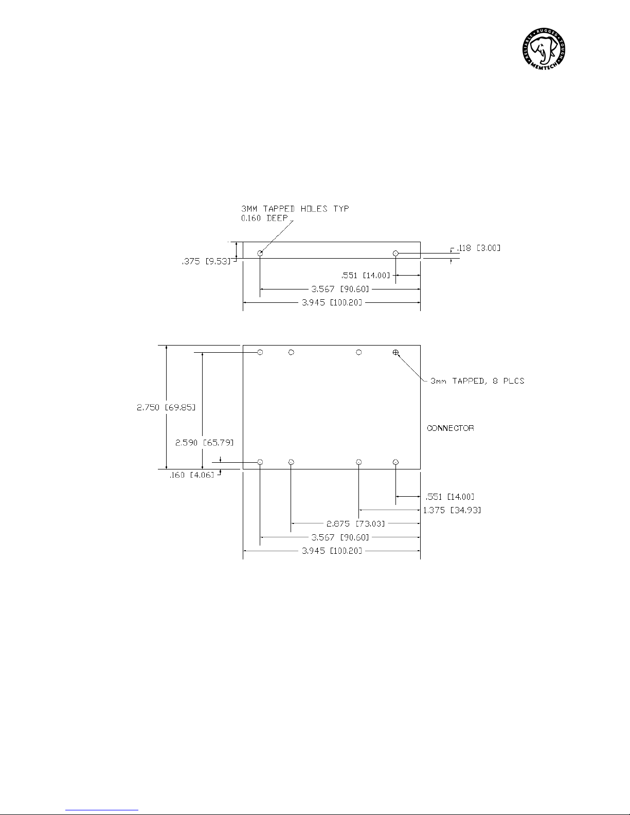
The AT2550 may be mounted in any orientation. Eight mounting holes are
available: four on the bottom and four on the sides. All holes are threaded 3mm,
with a maximum penetration of 4mm.
The diagram given below is for a 4.8 Gbyte drive. Drives with higher capacities
will be 12.5mm or taller. All other dimensions remain identical.
3.1.5 COMPUTER SETUP
To be recognized by the computer, the drive translation information must typically
be entered into the System Setup or CMOS Setup utility. For non-PC compatible
computers, this may not apply. The AT2550 supports automatic configuration if
offered by the BIOS. Automatic CHS translation and LBA mode is also supported.
AT2550 User Guide December 8, 2003 page 5 of 17
Page 6
3.1.6 PARTITION
The drive must be partitioned using the system’s FDISK utility. For operating
systems other than DOS, please refer to your OS operating guides. Note that
changing the partition information will erase all data currently on the drive. Refer
to your OS manual for information regarding partitioning a hard disk.
3.1.7 FORMAT
The AT2550 is low-level formatted at the factory, which establishes the 512-byte
sector size. A high-level format is required after the partition has been established
on the drive. Refer to your OS manual for information regarding hard disk drive
format procedures.
3.2 JUMPERS
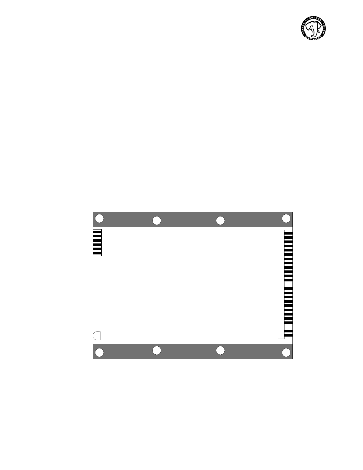
The following diagram illustrates the locations of the jumpers on the AT2550
controller card. The jumpers are found on both the J1 interface header and the J2
jumper header. Refer to the illustration below. The option jumpers control the
master/slave configuration of the drive, the use of cable selection, drive write
protection, and other factory related functions. All headers are on 2mm centers.
J2
XP
GND
TX/RX
OPT2
OPT1
WP
J1
LED
AT2550 User Guide December 8, 2003 page 6 of 17
AT2550 Bottom View
CS
M/S
Page 7
,
r
p
j
3.2.1 MAIN HEADER (J1) JUMPERS
J1 Connector View
Pin #1
J1 Header
2x25
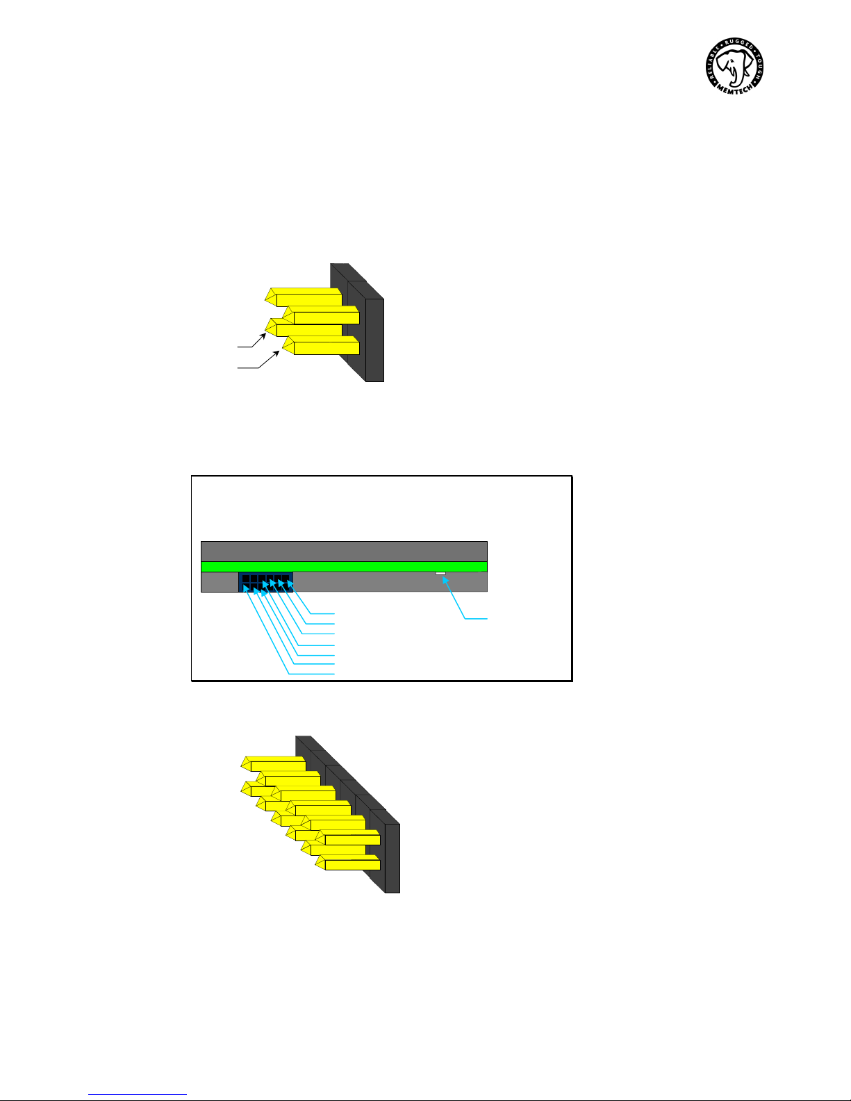
3.2.2 MASTER/SLAVE
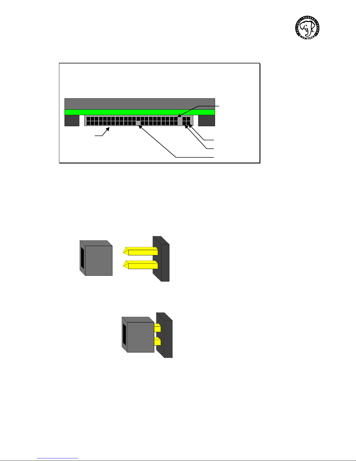
The MS jumper selects the drive as either the C: drive (Master) when off or the D:
drive (Slave) when installed. This jumper is part of the main ATA interface header
and is on 2mm centers. This location is factory shipped with no jumper,
configuring the drive as the master drive.
Connecting the pins forces the drive to drive D:, the slave.
MS Jumper
CS Jumpe
Key - pin 20
MS: Master/Slave
configured for normal
eration --jumper off
o
MS: Configured as Slave --
umper on
AT2550 User Guide December 8, 2003 page 7 of 17
Page 8
X
X
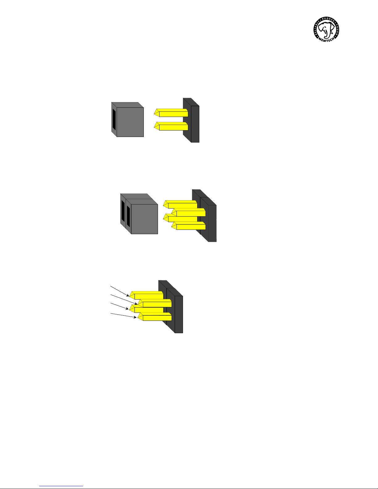
3.2.3 CABLE SELECT
Jumper CS can be used to let the IDE Cable Select signal select the drive
configuration as either the master or slave device. Shorting the CS pin to the MS
pin enables the Cable Select feature. Leaving the pins unconnected disables the
Cable Select feature. The drive is factory shipped with these pins open.
CS: Cable Select
configured for normal
operation -- jumper off
CS
MS
3.2.4 OPTION HEADER J2
The Option Header is located on the LED-side of the drive, as illustrated below:
J2 Option Jumpers,
2x6, 2mm
WP
OPT1
OPT2
GND
T
R
XP
LED
Jumper Header – J2
AT2550 User Guide December 8, 2003 page 8 of 17
Page 9
j
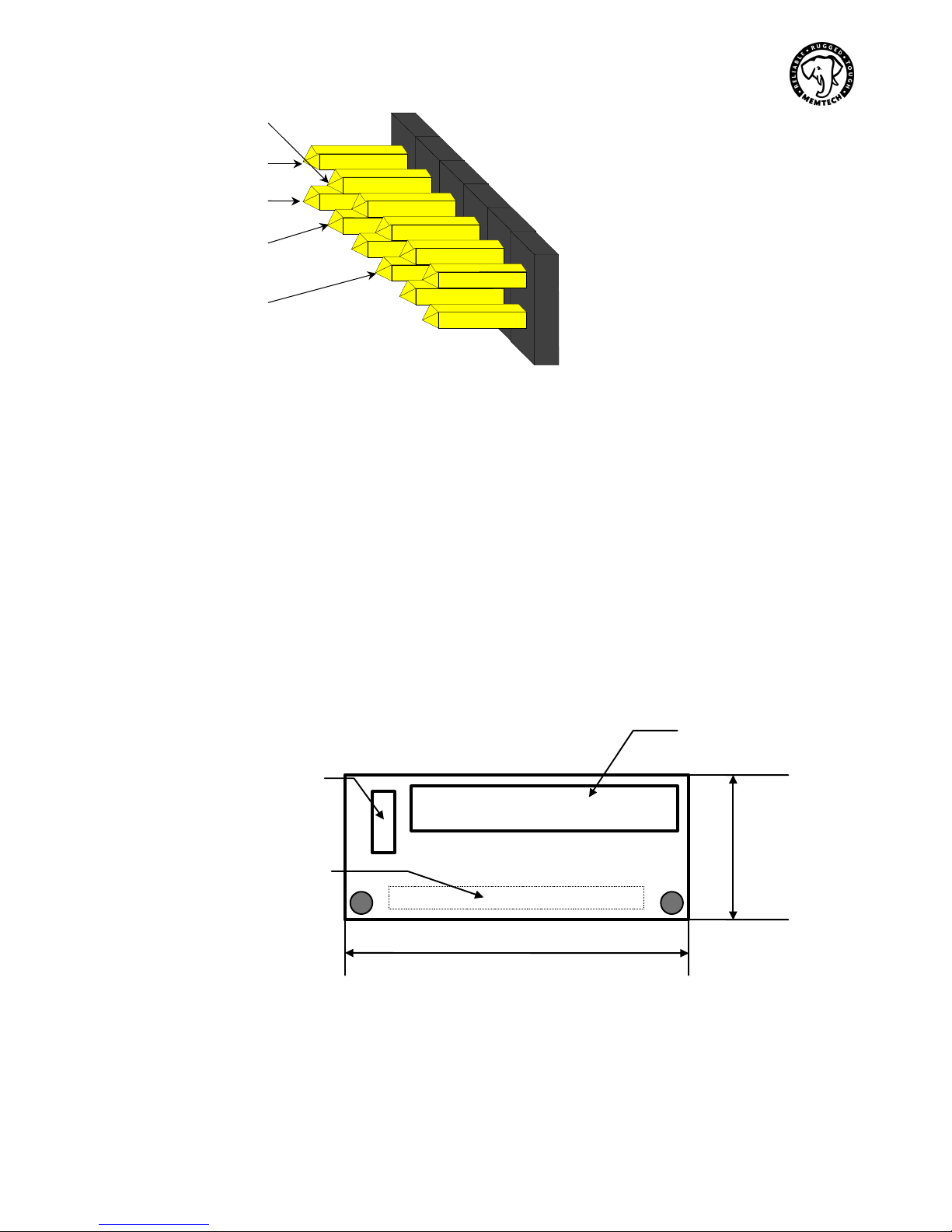
3.2.5 WRITE PROTECT
The WP jumper on header J2 is used to write-protect the drive. The default
position of this jumper is OFF. Installing the WP jumper inhibits all further writes
to the drive, while read accesses occur as normal.
3.2.6 OPTION JUMPERS
The OPT1 and OPT2 jumpers are used for factory test functions or special
functions only, and should always be left open.
WP: Write Protect
configured for normal
operation --
umper off
OPT1,2: Option Jumpers
configured for normal
operation -- jumpers off
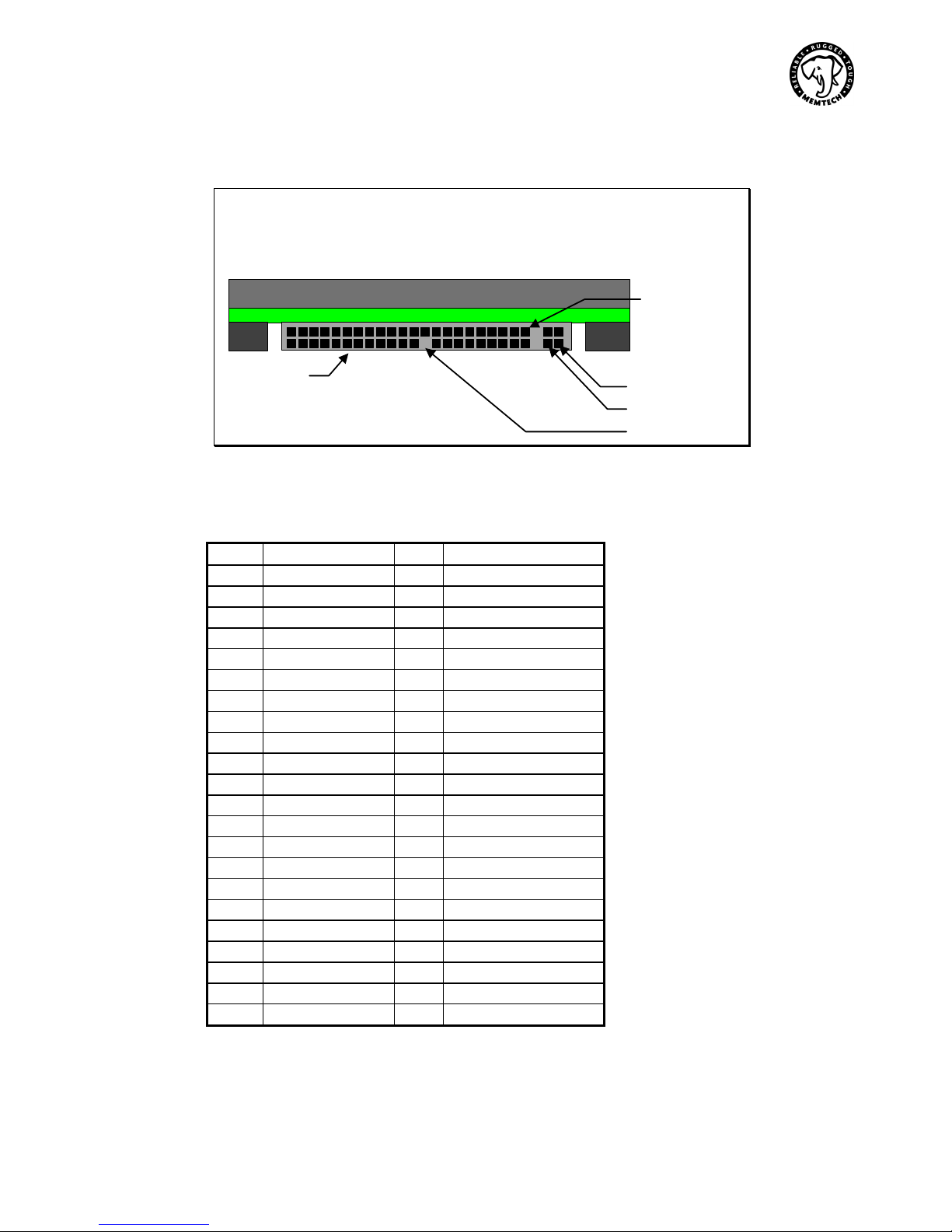
3.2.7 TX/RX CONNECTIONS
The TX and RX connections are for manufacturing use only.
GND
TX
GND
RX
3.2.8 EXTERNAL POWER
The XP pins on the Option Header are used to connect external standby power to
the drive. These pins are connected to the Kicker™ Holdup Circuit. Applied
power should be 5 volts +/- 10%. Do not exceed 6 volts on this line, as internal
damage to the drive may result.
The two outside pins on the header are used to connect power to the holdup
circuit. A third pin is needed to connect the grounds of the drive to the power
source.
TX/RX: RS232
Communications
AT2550 User Guide December 8, 2003 page 9 of 17
Page 10
GND
XP
XP
GND
GND
3.3 IDE INTERFACE
The AT2550 uses a 44-pin right angle 2mm connector mounted on the controller
PCB to create both a power and signal connection to the host. Maximum cable
length is 18 inches. Recommended cable length is 12 inches or less, especially if
an advanced PIO or UDMA transfer modes are being used. The recommended
mating socket connector is 3M 152244-003-GG or equivalent.
3.3.1 IDE ADAPTER
Jumper Header – J2
An adapter converting the 2mm IDE connector to a standard 40-pin 0.100” IDE
connector is available from the factory. Order part number 153264-002. The
adapter converts the signals from the 2mm connector on the drive to a 0.100”
connector. Power arrives via a 4-pin Amp power header (EI series) identical to the
connector used to supply power to 3.5 inch floppy drives. To convert the 4-pin
Amp power connector to a standard 4-pin AT power connector, request the ATA
power cable adapter, part number 153273-002.
COMP VIEW
Amp 4-pin
power
2mm 44-pin
socket - solder
side mount
2.75”
40-pin 0.100”
IDE
0.75”
AT2550 User Guide December 8, 2003 page 10 of 17
Page 11
,
3.3.2 IDE CONNECTOR PHYSICAL ORIENTATION
The diagram below depicts connector orientation and location.
J1 Connector View
Pin #1
J1 Header
2x25
3.3.3 IDE CONNECTOR PINOUT
The following table depicts the 44-pin, 2mm signal cable interface pin out.
PIN SIGNAL PIN SIGNAL
1 RESET- 2 GND
3 DATA7 4 DATA8
5 DATA6 6 DATA9
7 DATA5 8 DATA10
9 DATA4 10 DATA11
11 DATA3 12 DATA12
13 DATA2 14 DATA13
15 DATA1 16 DATA14
17 DATA0 18 DATA15
19 GND 20 KEY (NO PIN)
21 DRQ 22 GND
23 IOW- 24 GND
25 IOR- 26 GND
27 IOCHRDY 28 CSEL
29 DACK- 30 GND
31 IRQ 32 IOCS1633 ADDR1 34 PDIAG35 ADDR0 36 ADDR2
37 CS0- 38 CS139 DASP- 40 GND
41 +5VOLTS 42 +5VOLTS
43 GND 44 RESERVED
MS Jumper
CS Jumper
Key - pin 20
AT2550 User Guide December 8, 2003 page 11 of 17
Page 12

4. OPERATION
4.1 ACTIVE REMAP™ AND WRITE LIMITATIONS
Unlike mechanical drives, wherein the wear-out mechanism results from starting
and stopping the platters and the rotation of the spindle motors, the wear-out
mechanism for any solid state flash drive resides in writing to the non-volatile
memory, which in Memtech's case is NAND E
devices requires that electrons be first removed from, and then trapped on the
floating gate in each cell using Fowler-Nordheim tunneling techniques. This
process is inherently harsh on the oxide layer isolating the floating gate from the
silicon substrate in the device, and establishes the write cycle endurance of each
cell in a device as specified by the device manufacturer.
To overcome this limitation, Memtech Solid State Flash Drives have been
designed with Active Remap™, which, on a detected cell failure, moves the
entire failing block to a reserved location and maps the failing block out of
active memory. This process is automatic and invisible to the user. It
extends the device's useful life almost 100 fold, and makes the Memtech
series of Solid State Drives suitable for both read mostly and read/write
applications.
In an ongoing effort to determine the durability of the flash components and
in turn extend the life of our products, Memtech has also conducted several
endurance tests using our flash drives. The results were very
encouraging. During testing, done under both benign and harsh operating
conditions, Memtech observed and documented an erase/write cycle
endurance of 8 to 30 million cycles. This is compared to the flash
manufacturer's test and report of only 100,000 to 250,000 erase/write
cycles for the flash devices.
Reading the NAND E
oxide layers, and is therefore unlimited.
4.2 ECC
2
PROM has no adverse effects on the storage cells or
2
PROM. Writing the to the memory
The NRZ data interface used by the IDE controller implements a CRC/ECC
mechanism to detect and correct any errors in the data stored in the flash. This
polynomial is capable of correcting three 8-bit data bursts in a single sector, and
detecting up to six 8-bit error bursts per sector.
An extensive retry algorithm is implemented on the AT2550, so that single event
disturbances such as ESD can be readily overcome. Probability of miscorrection
is approximately 10
AT2550 User Guide December 8, 2003 page 12 of 17
-20
per bit corrected for a 512-byte field.
Page 13
4.3 POWER
4.3.1 POWER DOWN
Whenever possible, do not power down the computer during a write command
sequence to any mass storage device. This includes during the normal operation
of the drive, and with the use of disk cache programs such as Microsft
SmartDrive. If a write routine must interrupted, use the push button reset or a soft
reset. Powering down the AT2550 while it is being written may cause an
incomplete write sequence, and leave as many as 32 sectors with an Address
Mark Found Error or Uncorrectable Errors. DOS will report these with a message
“Error Reading Drive C:”.
4.3.2 POWER SUPPLY
The AT2550 voltage requirement is specified at +5 volts, +/- 5% on the drive itself.
Operation outside of these limits is not guaranteed. Note that the drive will
“operate” down to 4 volts, but reliability issues such as Uncorrectable Errors or
invalid data reads may occur. An on board voltage monitor will inhibit writes when
the supply voltage falls below 4.70 volts, thus preserving data integrity on the
drive.
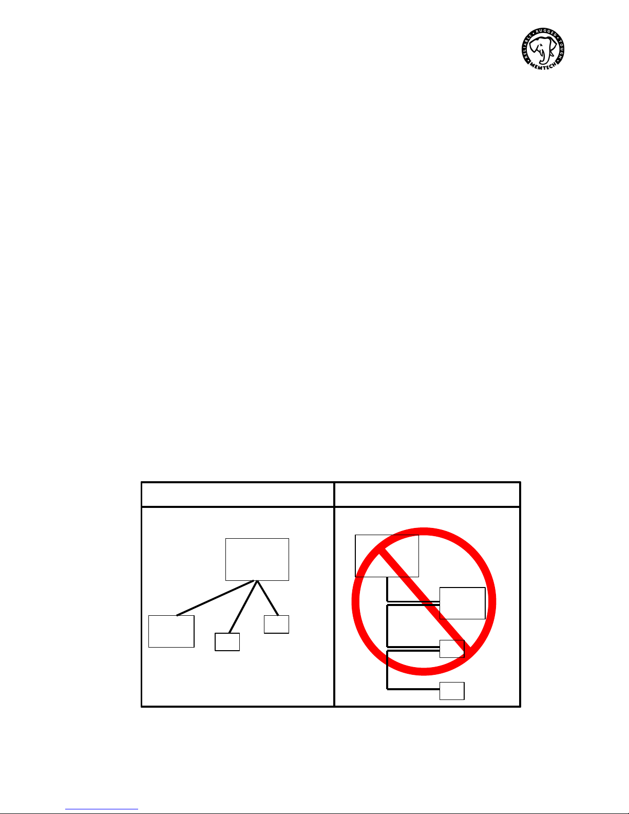
4.3.3 POWER ROUTING
®
To avoid “glitches” or noise on the Vcc and ground lines, power in the system
should be routed so that all peripherals are sourced directly from the power supply
as opposed to routing a single continuous supply line to each device in the system
as in daisy chaining. Routing power in the star configuration, as is done on most
desktop PCs, will minimize the effect of one device’s current draw on another
device. This is key to maintaining data integrity on the AT2550. See diagrams
below.
Star Topology Daisy Chain - Do Not Use
Power Supply
Main Board
Hard Disk
Floppy
Main Board
Power Supply
Floppy
Hard Disk
AT2550 User Guide December 8, 2003 page 13 of 17
Page 14
4.4 TROUBLE SHOOTING GUIDE
4.4.1 SELF-TEST DIAGNOSTIC CODES
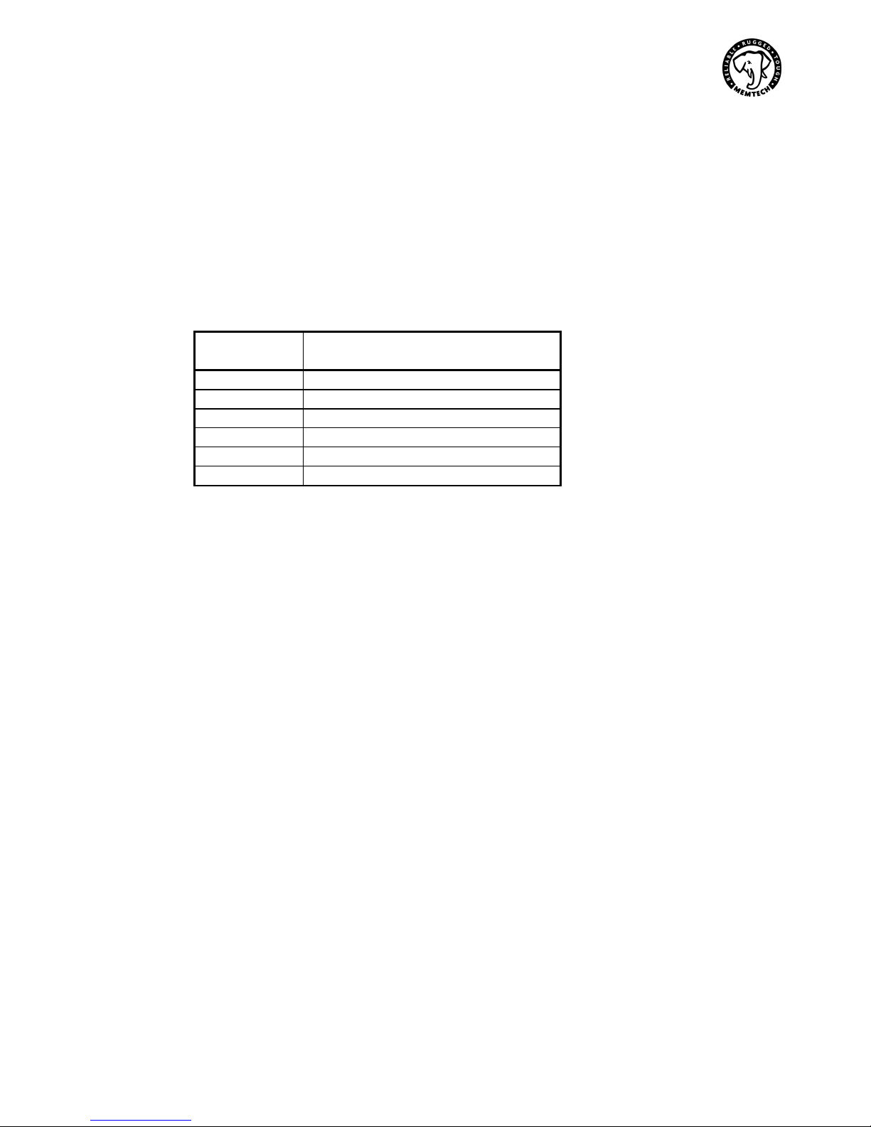
The AT2550 has been designed to issue blink codes via the LED in the event of a
low-level or catastrophic failure. A blink code of five would be defined as five fast
blinks, a pause with no blinks, and a repeat of the process. The drive will not
respond to commands or a soft reset when in this state. Only powering down the
drive will clear the drive state and restart internal diagnostics.
Blink codes and their associated failure mechanisms are defined below. In the
event a blink code is encountered, contact the factory for further assistance.
Number of
Blinks
2 ROM Firmware Checksum error
3 ASIC initialization error
4 SRAM Test failed
5 IDE buffer failure
6 IDE controller error
7 NRZ data path error
4.4.2 UNCORRECTABLE ERRORS
Error
If a drive has been subjected to a power down during a write command, or as
been run under marginal or dirty power conditions, uncorrectable errors may be
introduced into the media. This may result in data read errors, a corrupted FAT
table entry or directory, or an invalid boot partition or partition table. Microsoft
Scandisk or Norton Disk Doctor
partition table errors, but should not be allowed to mark a sector in the data area
as bad. On a rewrite to a data sector with uncorrectable errors, all synchronization
and ECC codes will be rewritten and the error will be eliminated.
5. MAINTENANCE
No maintenance is required during the normal use of this drive.
If data is to be archived for long periods of time (> 10 years), it is recommended
that the data on the drive be refreshed every 5 to 10 years. The manufacturer of
the NAND E
years. Programs such as Norton Speedisk
drive, or Microsoft
during its surface test, achieve this end very well.
2
PROM devices will only guarantee data integrity for a period of 10
™
will successfully correct FAT table problems and
©
®
Scandisk, which writes and reads every sector on the disk
, which reallocates all sectors on the
®
AT2550 User Guide December 8, 2003 page 14 of 17
Page 15

6. SPECIFICATIONS
6.1 INTERFACE
IDE Compatibility ATA6 - T13/1410Dr2a
IDE Drive Number Drive 0 or 1
Raw Physical Capacity 4864 Mbytes under 9.5mm
8704 Mbytes under 12.5mm
27904 Mbytes maximum
Physical Sector Size 512 bytes
6.2 PERFORMANCE
Average Access 0.1 ms
Track/Track Access 0.1 ms
Onboard Cache 16 Mbytes
Burst Transfer Rate 66 Mbytes/sec
Cached Read Transfers 26 Mbytes/sec
Cached Write Transfers 20 Mbytes/sec
6.3 ENVIRONMENTAL
Commercial Temperature Range
Operating 0
Storage -45
Extended Temperature Range (E)
Operating -20
Storage -45
Industrial Temperature Range (I)
Operating -40
Storage -55
Military Temperature Range (M)
Operating -55
Storage -55
Shock - operating 1000G, half sine (target)
Vibration - operating 15G Random (target)
Airflow None required
Humidity 5% to 95% NC (target)
6.4 POWER REQUIREMENTS
Voltage 5V +/- 5%
Current 4.8 Gbyte drive
Idle 200 mA
Read 350 mA
Write 320 mA
o
to 70o C
o
C to 125o C
o
C to 75oC
o
C to 125o C
o
to 85o C
o
to 125o C
o
to 125o C
o
to 125o C
AT2550 User Guide December 8, 2003 page 15 of 17
Page 16

6.5 MECHANICAL
Length 3.95 inches (100 mm)
Width 2.75 inches (70 mm)
Height -
4864 to 8704 Mbytes 0.49 inches (12.5 mm)
4864 Mbytes 0.37 inches (9.5 mm)
<
Cable Interface 44-pin, 2mm
Max. Cable Length 12 inches (305 mm)
Rec. Cable Length 8 inches (203 mm)
Weight (4.8 Gbytes) 3.5oz (98g)
6.6 RELIABILITY
6.6.1 ERROR CORRECTION
Programmable 96-bit Reed-Solomon Error Correction and Detection capable of
correcting three random byte errors per sector.
6.6.2 MEMORY CELL ENDURANCE
8 million write/erase cycles (excluding ECC and Active Remap™).
6.6.3 DRIVE ENDURANCE
800 million write/erase cycles minimum with ECC and Active Remap™ enabled.
Read endurance is unlimited.
AT2550 User Guide December 8, 2003 page 16 of 17
Page 17

7. APPENDIX
7.1 CONTACT INFORMATION
For Technical Support or Warranty Repair information, please contact Memtech
at:
Memtech Technology
7628 Las Positas Road
Livermore, CA U.S.A. 94551
phone: (925) 294-8483
toll free: (800) 445-5511
7.2 ATA SPECIFICATION INFORMATION
Information regarding the ATA6 specification may be obtained from the following
locations:
AT-Attachment Document Distribution
Global Engineering
15 Inverness Way East
Englewood, Co. 80112-5704
Phone: (303) 792-2181 or (800) 854-7179
Fax: (303) 792-2192
ATA Anonymous FTP Site
http://fission.dt.wdc.com
7.3 LIMITED LIFETIME WARRANTY
Memtech warrants your AT2550 against defects in material and workmanship for
the life of the drive. The warranty is void in the case of misuse, accident,
alteration, improper installation, misapplication or the result of unauthorized
service or repair.
The implied warranties of merchantability and fitness for a particular purpose, and
all other warranties, expressed or implied, except as set forth in this warranty,
shall not apply to the products delivered.
In no event shall Memtech be liable for any lost profits, lost savings or other
incidental or consequential damages arising out of the use of, or inability to use,
this product.
BEFORE RETURNING PRODUCT, A RETURN MATERIAL AUTHORIZATION
(RMA) MUST BE OBTAINED FROM MEMTECH.
Product shall be returned to Memtech with shipping prepaid. If the product fails to
conform and warranty repair is necessary, Memtech will reimburse customer for
the transportation charges incurred.
AT2550 User Guide December 8, 2003 page 17 of 17
 Loading...