

Page 1
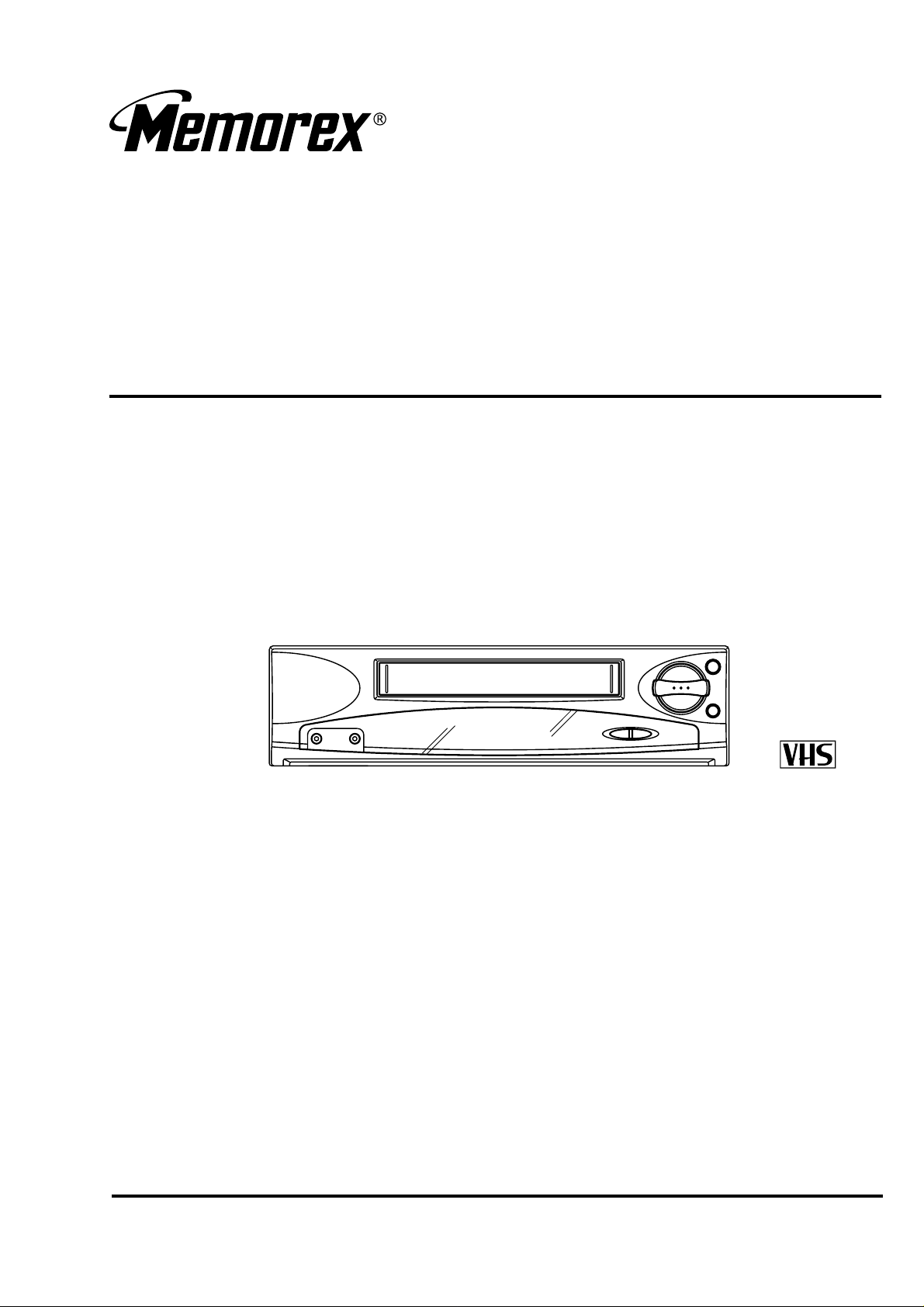
MVR2031
SERVICE MANUAL
VIDEO CASSETTE RECORDER
ORIGINAL
MFR’S VERSION A
Design and specifications are subject to change without notice.
Page 2
SERVICING NOTICES ON CHECKING
1. KEEP THE NOTICES 3. PUT PARTS AND WIRES IN THE
As for the places which need special attentions,
they are indicated with the labels or seals on the
cabinet, chassis and parts. Make sure to keep the
indications and notices in the operation manual.
2. USE THE DESIGNATED PARTS
The parts in this equipment have the specific
characters of incombustibility and withstand
voltage for safety. Therefore, the part which is
replaced should be used the part which has
the same character.
Especially as to the important parts for safety
which is indicated in the circuit diagram or the
table of parts as a mark, the designated
parts must be used.
!
ORIGINAL POSITION AFTER
ASSEMBLING OR WIRING
There are parts which use the insulation
material such as a tube or tape for safety, or
which are assembled in the condition that
these do not contact with the printed board.
The inside wiring is designed not to get closer
to the pyrogenic parts and high voltage parts.
Therefore, put these parts in the original
positions.
PERFORM A SAFETY CHECK AFTER
4.
SERVICING
Confirm that the screws, parts and wiring which
were removed in order to service are put in the
original positions, or whether there are the
portions which are deteriorated around the
serviced places serviced or not. Check the
insulation between the antenna terminal or
external metal and the AC cord plug blades.
And be sure the safety of that.
HOW TO ORDER PARTS
Please include the following informations when you order parts. (Particularly the VERSION LETTER.)
1. MODEL NUMBER and VERSION LETTER
The MODEL NUMBER can be found on the back of each product and the VERSION LETTER can be
found at the end of the SERIAL NUMBER.
2. PART NO. and DESCRIPTION
You can find it in your SERVICE MANUAL.
A1-1
Page 3

CONTENTS
SERVICING NOTICES ON CHECKING .....................................................................................
HOW TO ORDER PARTS .............................................................................................................
CONTENTS ................................................................................................................................
GENERAL SPECIFICATIONS.......................................................................................................
DISASSEMBLY INSTRUCTIONS
1. REMOVAL OF MECHANICAL PARTS AND P. C. BOARDS.............................................. .
2. REMOVAL OF DECK PARTS...............................................................................................
3. REMOVAL AND INSTALLATION OF FLAT PACKAGE IC ..................................................
KEY TO ABBREVIATIONS ...........................................................................................................
SERVICE MODE LIST ...................................................................................................................
PREVENTIVE CHECKS AND SERVICE INTERVALS.................................................................
SERVICING FIXTURES AND TOOLS ..........................................................................................
PREPARATION FOR SERVICING................................................................................................
MECHANICAL ADJUSTMENTS ...................................................................................................
ELECTRICAL ADJUSTMENTS.....................................................................................................
BLOCK DIAGRAMS
Y/C/AUDIO/CCD/HEAD AMP ....................................................................................................
SYSTEM CONTROL/SERVO.....................................................................................................
TUNER........................................................................................................................................
OPERATION/POWER ................................................................................................................
PRINTED CIRCUIT BOARDS
SYSCON/OPERATION ..............................................................................................................
SCHEMATIC DIAGRAMS
Y/C/AUDIO/CCD/HEAD AMP ....................................................................................................
SYSTEM CONTROL/SERVO.....................................................................................................
POWER ......................................................................................................................................
OPERATION...............................................................................................................................
TUNER........................................................................................................................................
INTERCONNECTION DIAGRAM ..................................................................................................
WAVEFORMS ................................................................................................................................
MECHANICAL EXPLODED VIEW ................................................................................................
CHASSIS EXPLODED VIEWS ......................................................................................................
MECHANICAL REPLACEMENT PARTS LIST ............................................................................
CHASSIS REPLACEMENT PARTS LIST.....................................................................................
ELECTRICAL REPLACEMENT PARTS LIST............................................................................
A1-1
A1-1
A2-1
A3-1~A3-4
B1-1
B2-1~B2-6
B3-1, B3-2
C1-1, C1-2
C2-1
C3-1
C4-1
C4-1
D1-1~D1-4
D2-1, D2-2
E-1, E-2
E-3, E-4
E-5, E-6
E-7, E-8
F-1 ~ F-4
G-1, G-2
G-3, G-4
G-5, G-6
G-7, G-8
G-9, G-10
G-11, G-12
H-1
I-1
I-2, I-3
J1-1
J2-1
J3-1
A2-1
Page 4
GENERAL SPECIFICATIONS
G-1 VCR System VHS Player / Recorder
G-2 Tuning Broadcasting System US System M
G-3 Power Power Source AC 120V,60Hz
G-4 Regulation Safety UL
G-5 Temperature Operation 5oC - 40oC
G-6 Operating Humidity Less then 80% RH
G-7 Signal Video Signal Input Level 1 V p-p/75 ohm
G-8 On Screen Menu Yes
System Video System NTSC
System Tuner and System 1Tuner
Display Menu Type Character
Hi-Fi STEREO No
NTSC PB(PAL60Hz) No
Deck DECK OVD-7
Heads Video Head 4Head
FM Audio Head No
Normal Audio /Control Mono / Yes
Erase(Full Track Erase) Yes
Tape Rec PAL Speed NTSC SP/SLP
Play PAL -
Fast Forward / Rewind Time (Approx.) FF:4'50"/REW:2'30"
Forward/Reverse NTSC or PAL-M SP/LP/SLP=3x,5x/7x,9x/9x,15x
Picture Search PAL or SECAM Frame Advance Slow 1/10
Slow Speed Variable Slow 1/10
Receive CH Destination USA(w/CATV)
Intermediate Picture(FP) 45.75MHz
Frequency Sound(FS) 41.25MHz
Preset CH No
RF Converter Output Yes
Channel 3 or 4 ch
Level/Impedance 66dBu /75ohm
Sound Selector No
Stereo/Dual TV Sound No
Power Consumption Power On(at AC) 8W at 120V 60Hz
Protector Power Fuse Yes
Audio Signal Input Level -8dB/50Kohm
(0dB=0.775Vrms) Output Level -8dB/1Kohm
Hi-Fi Audio Signal Dynamic Range : More than -
ATS No
Timer Rec Set Yes
Auto Repeat On/Off Yes
SAP On Off No
CH Set-Up Yes
Loading System Front
Motor 3
NTSC SP/LP/SLP
with Cassette T-120
Tuning System F-Synth
Input Impedance VHF/UHF 75 OHM
CH Coverage
FP-FS 4.50MHz
DC -
Stand by (at AC) 1.8W at 120V 60Hz
Per Year - kWh/Year
Dew Sensor No
Radiation FCC
Storage -20oC - 60oC
Output Level 1 V p-p/75 ohm
S/N Ratio (Weighted) 50
Horizontal Resolution at SP Mode 230Line
S/N Ratio at SP (Weighted) 42dB
Harmonic Distortion (1KHz) 1.5%
Frequency Response at SP 100Hz - 10kHz
at LP 100Hz - 6kHz
at SLP 100Hz - 4kHz
Frequency Response Wow And Flutter : Less than Channel Separation : More than Harmonic Distortion : Less than -
TV/CATV Yes
Auto CH Memory Yes
Add/Delete Yes
2-69,4A,A-5~ A-1,A~I, J~ W
W+1~W+84
A3-1
Page 5
GENERAL SPECIFICATIONS
(
Pin Code Registration No
System Set-Up No
Clock Set Yes (Calendar 12H)
Language Yes
G-CODE(or SHOWVIEW or PLUSCODE)No. Entry No
NICAM 1/2,NICAM Off,Audio Output No
Stereo,Audio Output,SAP No
Play/Stop/FF/Rew/Rec/OTR/T-Rec/Pause/Eject/Tape In (Symbol Mark)
G-9 OSD Language English French Spanish
G-10 Clock,Timer Calendar 1990/1/1 ~ 2081/12/31
and Timer Timer Events 8 prog/1 month
Back-up One Touch Recording Max Time 5 Hours
OTPB Valid Time No
Timer Back-up (at Power Off Mode) 5 sec.
G-11 Display Indicator No
Indicator Type -
G-12 Remote Unit RC-EA
Control Glow in Dark Remocon No
Power Source Voltage(D.C) 3V
Total Keys 32 Keys
Keys Power Yes
No Noise Back Ground Yes
Yes
CH/AV Yes
Clock Yes
Repeat Yes
Pin Code No
Tape Counter Yes
Index No
Hotel Lock No
Tape Speed Yes
Manual Tracking (Bar Setting) No
Hi-Fi No
S-Repeat/SR-R/SR-Play No
VPS No
PDC No
OSD Language Setting English
Clock/Counter,CH,Timer Rec,OTR, Play
Cue),Rew(Rev),Stop,ATR
Rec,FF
Pause("Rec"Flash) Still("Play"Flush) Eject(Tape Mark Flash) Slow WKL,Y.M.D,Start,End AFT Repeat A-DUB VCR Memory Index VPS PDC SP LP SLP AM PM -
F1,F2
RF Output CH -
UM size x pcs UM-4 x 2 pcs
1 Yes
2 Yes
3 Yes
4 Yes
5 Yes
6 Yes
7 Yes
8 Yes
9 Yes
0 Yes
CH Up Yes
CH Down Yes
Input Select Yes
Play Yes
F.Fwd Yes
Rew Yes
Pause/Still Yes
Stop Yes
-
-
A3-2
Page 6
GENERAL SPECIFICATIONS
Rec/OTR Yes
Eject No
Counter Reset Yes
Speed Yes
Timer Rec Yes
TV Monitor No
Quick View No
Program No
Slow Yes
Auto Tracking Yes
Set/Tracking+ Yes
Set/ Tracking - Yes
Menu Yes
Enter Yes
Cancel Yes
Call Yes
TV/VCR Yes
Sleep Timer No
Muting No
Clock/Counter No
Zero Return No
CM Skip No
G-13 Features Auto Head Cleaning Yes
Auto Tracking Yes
Index Search No
HQ (VHS Standard High Quality) Yes
Auto Power On, Auto Play, Auto Rewind, Auto Eject Yes
Auto Power Off Yes
Forward/Reverse Picture Search Yes
VIDEO PLUS+(SHOWVIEW,G-CODE) No
ATS No
PDC No
VPS No
One Touch Playback No
Picture Control No
Auto Preset No
Channel Lock No
Hotel Lock No
Anti Theft No
Audio Dubbing No
Remort Control Code 1/2 No
SQPB No
CATV Yes
Energy Star Yes
MTS(SAP) No
CM Skip(30sec x 6 Times) No
G-14 Accessories Owner's Manual Language English/Spanish
Remote Control Unit Yes
Dew Cation Sheet No
Video Cassette Tape No
Battery No
Audio Select No
w/Guarantee Card No
UM size x pcs -
Safety Tip No
Toll Free Insert Sheet No
Quick Set-Up Sheet No
Information Sheet (Buyer Supply) No
75 Ohm Coaxial Cable Yes(Single shield)
Rod Antenna No
Loop Antenna No
U/V Mixer No
DC Car Cord (Center+) No
Guarantee Card Yes
Warning Sheet No
Circuit Diagram No
Antenna Change Plug No
Service Facility List No
Important Safeguard No
Dew/AHC Caution Sheet No
AC Plug Adapter No
Quick Set-up Sheet No
AC Cord No
Poles
Terminal
Terminal
A3-3
Page 7
GENERAL SPECIFICATIONS
AV Cord (2Pin-1Pin) No
Registration Card No
PTB Sheet No
Tape Rewinder(Buyer Supply) No
G-15 Interface Switch Front Power Yes
G-16 Set Size Approx. W x D x H (mm) 360 x 229 x 95
G-17 Weight Net (Approx.) 3.2kg(7.1lbs)
G-18 Carton Master Carton No
G-19 Cabinet Material Cabinet Front PS 94V2 DECABROM
300 ohm to 75 ohm Antenna Adapter No
Play Yes
Pause/Still No
System Select No
One Touch Playback No
Channel Up Yes
Channel Down Yes
F.FWD/Cue Yes
Eject/Stop Yes
Main Power SW No
Volume Up No
Volume Down No
Rew/Rev Yes
Rec/OTR Yes
Rear RF Output SW Yes
Indicator Power Yes
Stand by No
Rec/OTR No
Repeat No
TV/VCR Yes
Rec Yes
T-Rec Yes
Tape In No
Terminals Front Video Input RCA x 1
Audio Input RCA x 1
Other Terminal No
Rear Video Input No
Audio Input No
Video Output RCA x 1
Audio Output RCA x 1
Euro Scart No
DC Jack 12V(Center +) No
VHF/UHF Antenna Input F Type
AC Inlet No
Gross (Approx.) 3.8kg(8.4lbs)
Content Material Dimensions W x D x H(mm) Description of Origin -
Gift Box Yes
Material Single/White
Dimensions W x D x H(mm) 420x291x160
Design As Per BUYER 's
Description of Origin Yes
Drop Test Natural Dropping At 1Corner / 3Edges / 6Surfaces
Height (cm) 80
Container Stuffing(40' container) 3136Sets
A3-4
Page 8
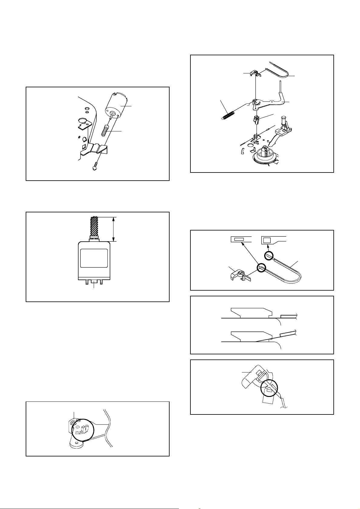
DISASSEMBLY INSTRUCTIONS
REMOVAL OF MECHANICAL PARTS
1.
AND P.C. BOARDS
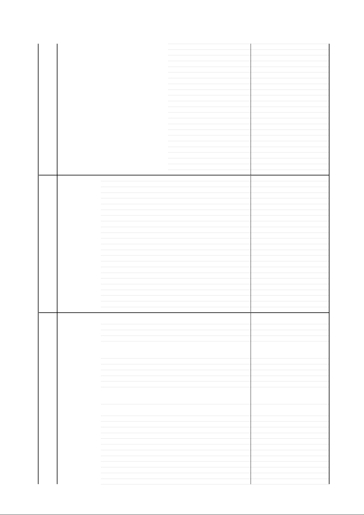
1-1: TOP CABINET, FRONT CABINET AND
OPERATION PCB (Refer to Fig. 1-1)
1.
Remove the 4 screws 1.
2.
Remove the Top Cabinet in the direction of arrow (A).
3.
Disconnect the following connector: (CP651).
4.
Unlock the 7 supports 2.
5.
Remove the Front Cabinet in the direction of arrow (B).
6.
Remove the 3 screws 3 and remove the Operation PCB.
1
Top Cabinet
1
(A)
1
Front Cabinet
2
2
1-2: FLAP (Refer to Fig. 1-2)
1.2.Open Flap to 90˚ and flex in direction of arrow (A), at
the same time slide in direction of arrow (B).
Then lift in direction of arrow (C).
(B)
2
2
2
2
3
3
3
Operation PCB
Fig. 1-1
1-3: DECK CHASSIS (Refer to Fig. 1-3)
Remove the 3 screws 1.
1.
Disconnect the following connectors: (CP1001, CP4001,
2.
CP4002 and CP4003).
Remove the Deck Chassis in the direction of arrow.
3.
1
1
1
Deck Chassis
1
Bottom Plate
Fig. 1-3
1-4: SYSCON PCB AND JACK PLATE (Refer to Fig. 1-4)
Remove the screw 1.
1.
Remove the screw 2.
2.
Remove the Syscon PCB in the direction of arrow.
3.
2
(C)
(B)
(A)
Flap
Syscon PCB
1
Bottom Plate
Fig. 1-4
Fig. 1-2
B1-1
Page 9
DISASSEMBLY INSTRUCTIONS
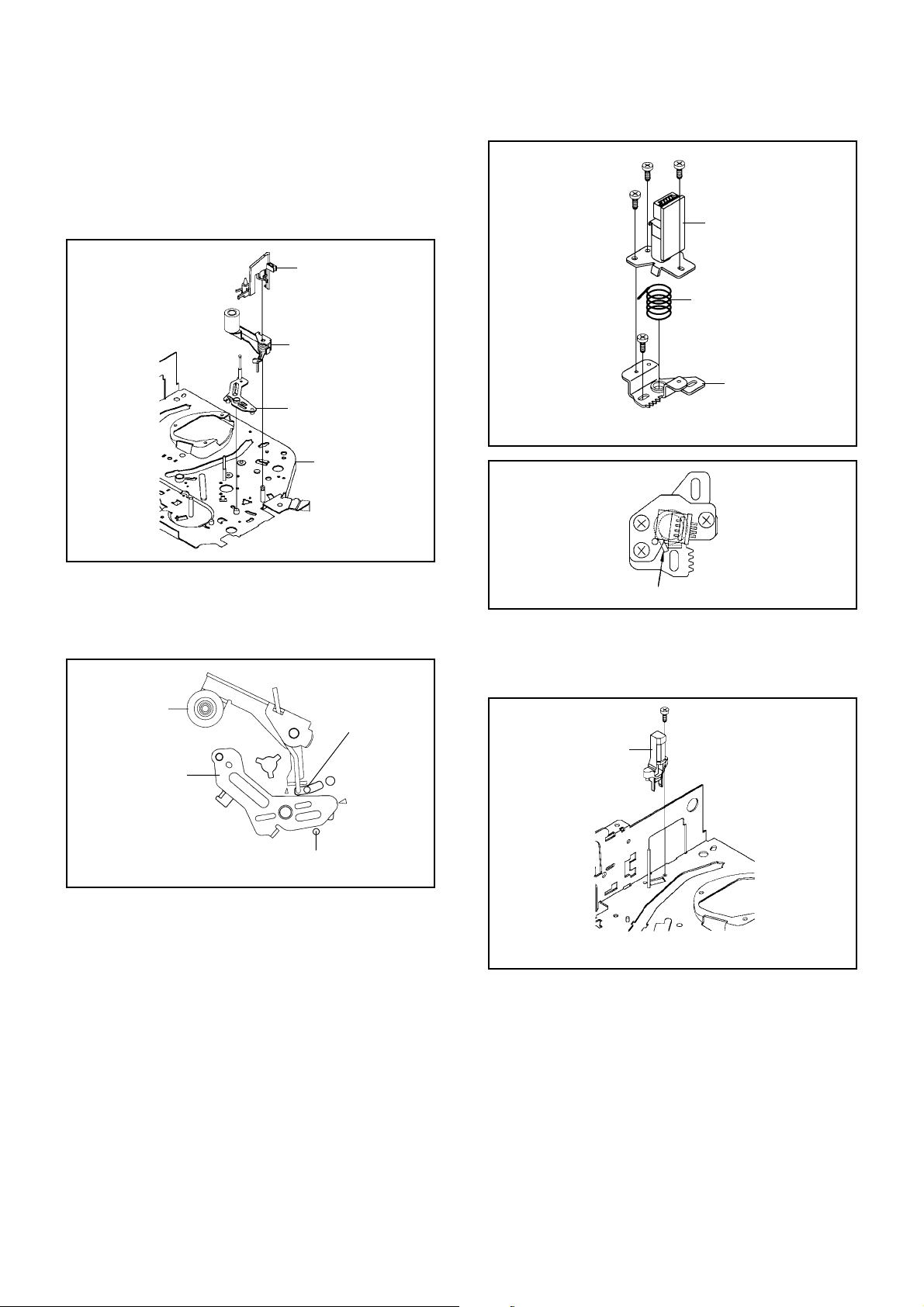
2. REMOVAL OF DECK PARTS
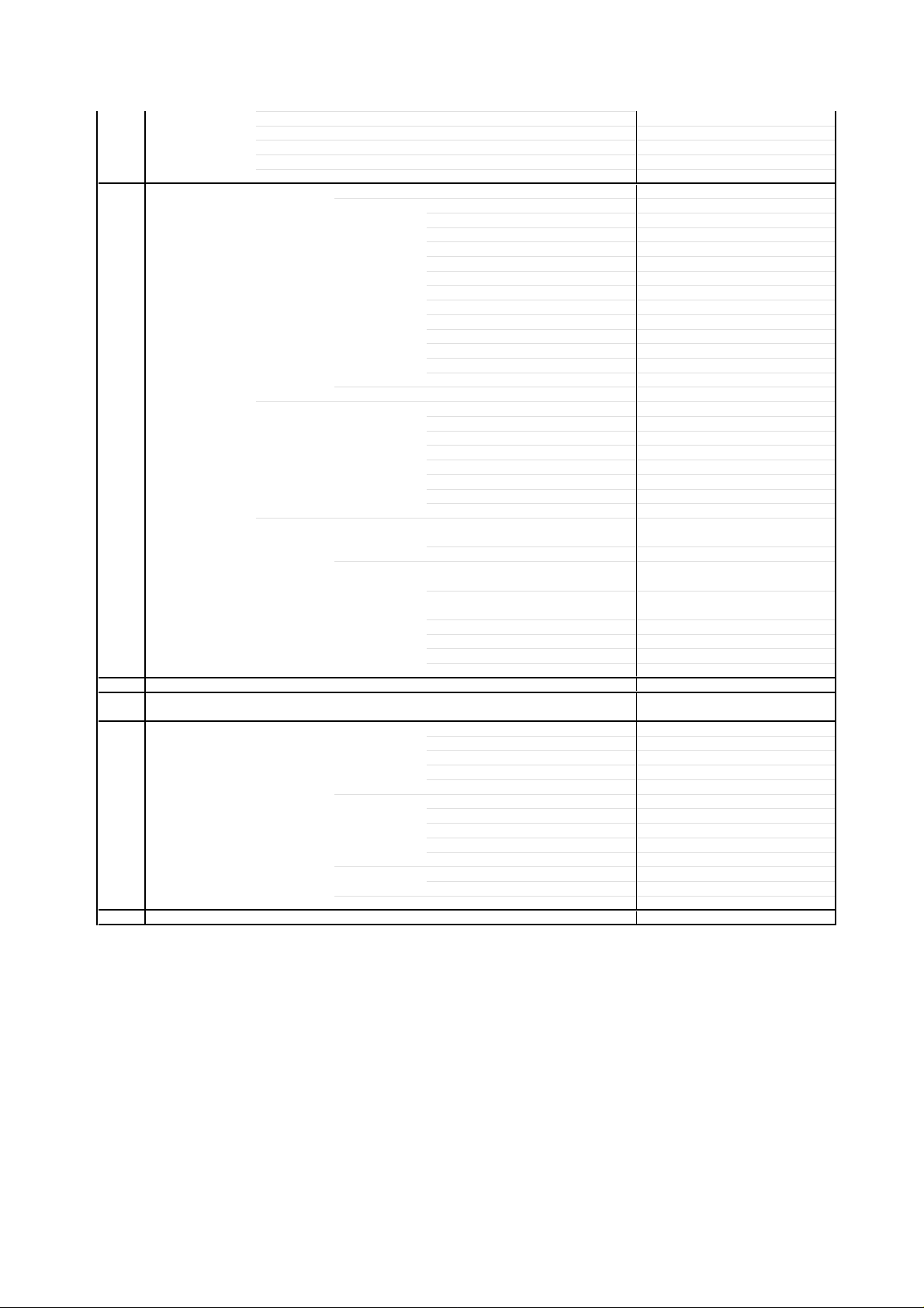
2-1: TOP BRACKET (Refer to Fig. 2-1)
Extend the 2 supports 1.
1.
Slide the 2 supports 2 and remove the Top Bracket.
2.
NOTE
1. After the installation of the Top Bracket, bend the
support 1 so that the Top Bracket is fixed.
Top Bracket
1
Top Bracket
2
Main Chassis
2
Main Chassis
2-2: CASSETTE HOLDER ASS'Y (Refer to Fig. 2-2)
Move the Cassette Holder Ass'y to the front side.
1.
Push the Locker R to remove the Cassette Side R.
2.
Remove the Cassette Side L.
3.
Main Chassis
Cassette Side R
1
Fig. 2-1
Locker R
NOTE
1.2.In case of the Locker R installation, check if the two
positions of Fig.2-3-B are correctly locked.
When you install the Cassette Side R, be sure to move
the Locker R after installing.
Locker R
Check if these
Cassette Side R
positions are locked.
Fig. 2-3-B
2-4: LINK UNIT (Refer to Fig. 2-4)
Set the Link Unit to the Eject position.
1.
Unlock the support 1.
2.
Remove the (A) side of the Link Unit first, then remove
3.
the (B) side.
Main Chassis
Link Unit
Link Ass'y
Cassette Side L
Main Chassis
Fig. 2-2
2-3: CASSETTE SIDE L/R (Refer to Fig. 2-3-A)
Remove the Locker Spring.
1.
Unlock the 4 supports 1 and then remove the Cassette
2.
Side L/R.
Unlock the support 2 and then remove the Locker R.
3.
Locker Spring
1
1
2
Cassette Holder
Locker R
1
1
(A)
1
(B)
Link Unit
Main Chassis
2-5: LINK LEVER/FLAP LEVER (Refer to Fig. 2-5)
Remove the Link Lever.
1.
Remove the Flap Lever.
2.
Flap Lever
Link Lever
Fig. 2-4
Fig. 2-5
Cassette Side R
Cassette Side L
Fig. 2-3-A
B2-1
Page 10
DISASSEMBLY INSTRUCTIONS
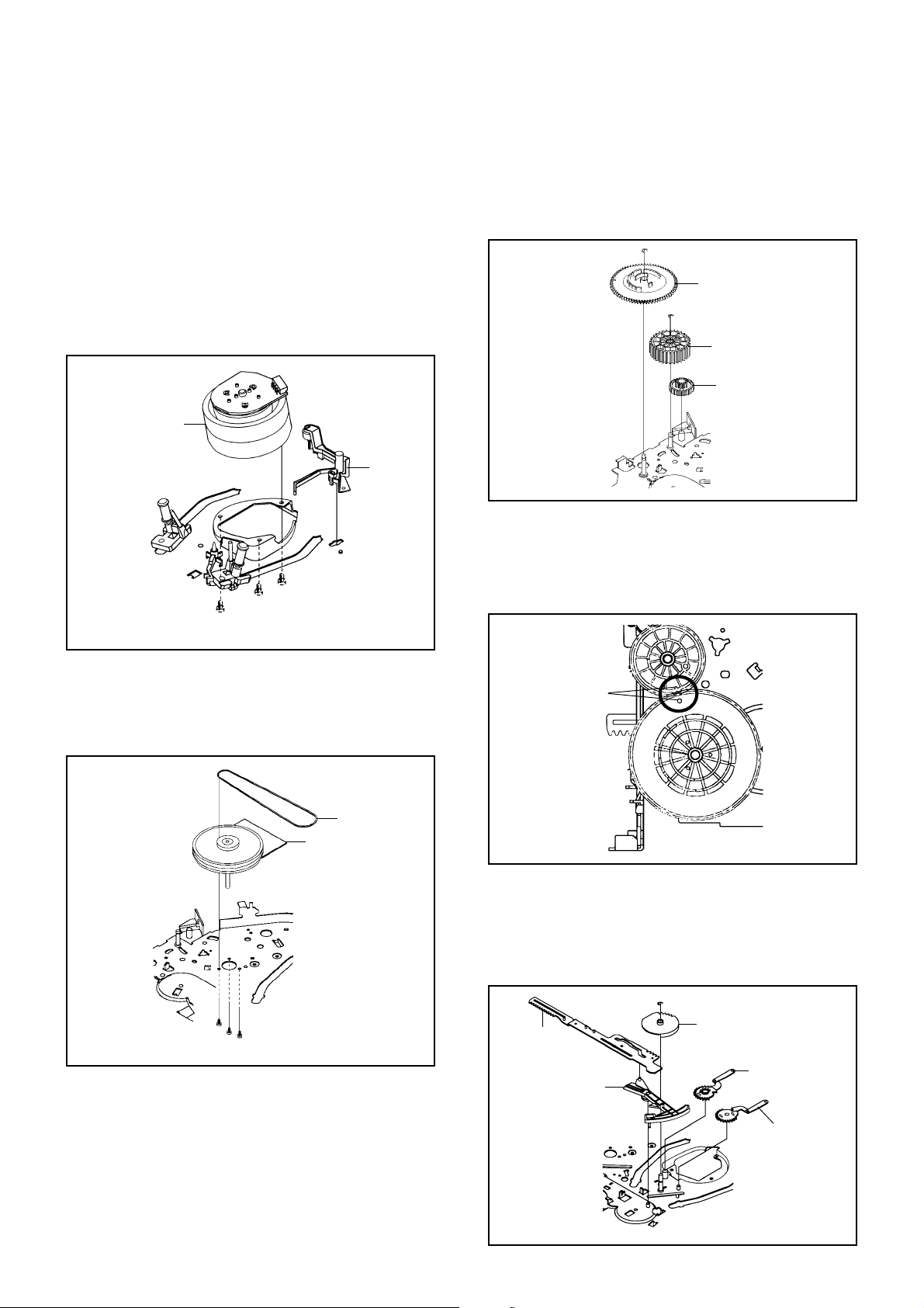
2-6: LOADING MOTOR/WORM (Refer to Fig. 2-6-A)
Remove the screw 1.
1.
Remove the Loading Motor.
2.
Remove the Worm.
3.
Loading Motor
Worm
Main Chassis
• Screw Torque: 3 ± 0.5kgf•cm
1
Fig. 2-6-A
NOTE
1. In case of the Worm installation, check if the value of
the Fig. 2-6-B is correct.
19.2 ± 0.1mm
1
Tension Connect
Tension Spring
2
4
1
3
Tension Holder
Tension Band
Tension Arm Ass'y
Fig. 2-7-B
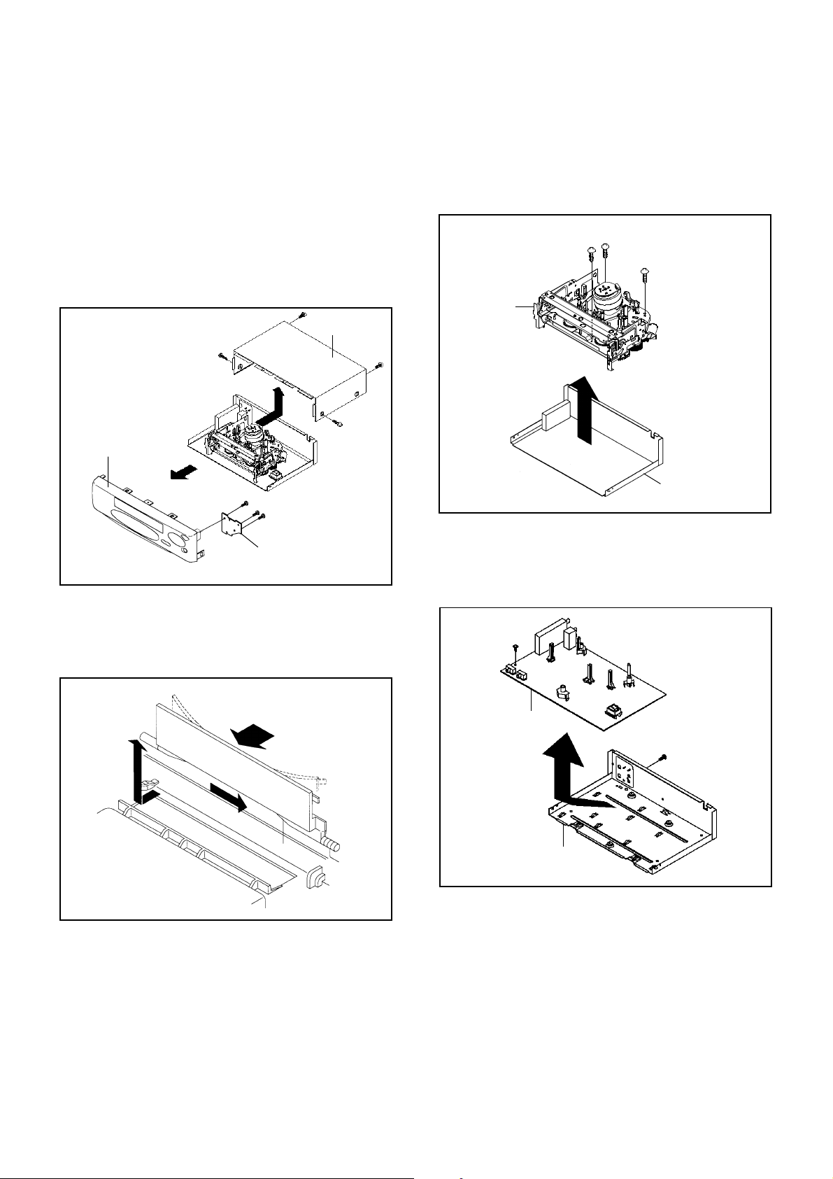
NOTE
1.
In case of the Tension Band installation, note the
direction of the installation. (Refer to Fig. 2-7-C)
2.
In case of the Tension Band installation, install correctly
as Fig. 2-7-D.
3.
In case of the Tension Connect installation, install as
the circled section of Fig. 2-7-E.
Safety surface for pressing
of the insert.
Fig. 2-6-B
2-7: TENSION ASS'Y (Refer to Fig. 2-7-B)
Turn the Pinch Roller Cam clockwise so that the
1.
Tension Holder hook is set to the position of Fig. 2-7-A
to move the Tension Arm Ass'y.
Remove the Tension Spring.
2.
Unlock the 2 supports 1 and remove the Tension
3.
Band.
Unlock the support 2 and remove the Tension Arm
4.
Ass'y.
Unlock the support 3 and remove the Tension
5.
Connect.
Float the hook 4 and turn it clockwise then remove the
6.
Tension Holder.
Tension Arm Ass'y
Tension Connect
[OK]
[NG]
Tension Connect
Tension Connect
Tension Connect
Main Chassis
Tension Band
Fig. 2-7-C
Tension Band
Tension Band
Fig. 2-7-D
Fig. 2-7-E
Fig. 2-7-A
B2-2
Page 11

DISASSEMBLY INSTRUCTIONS
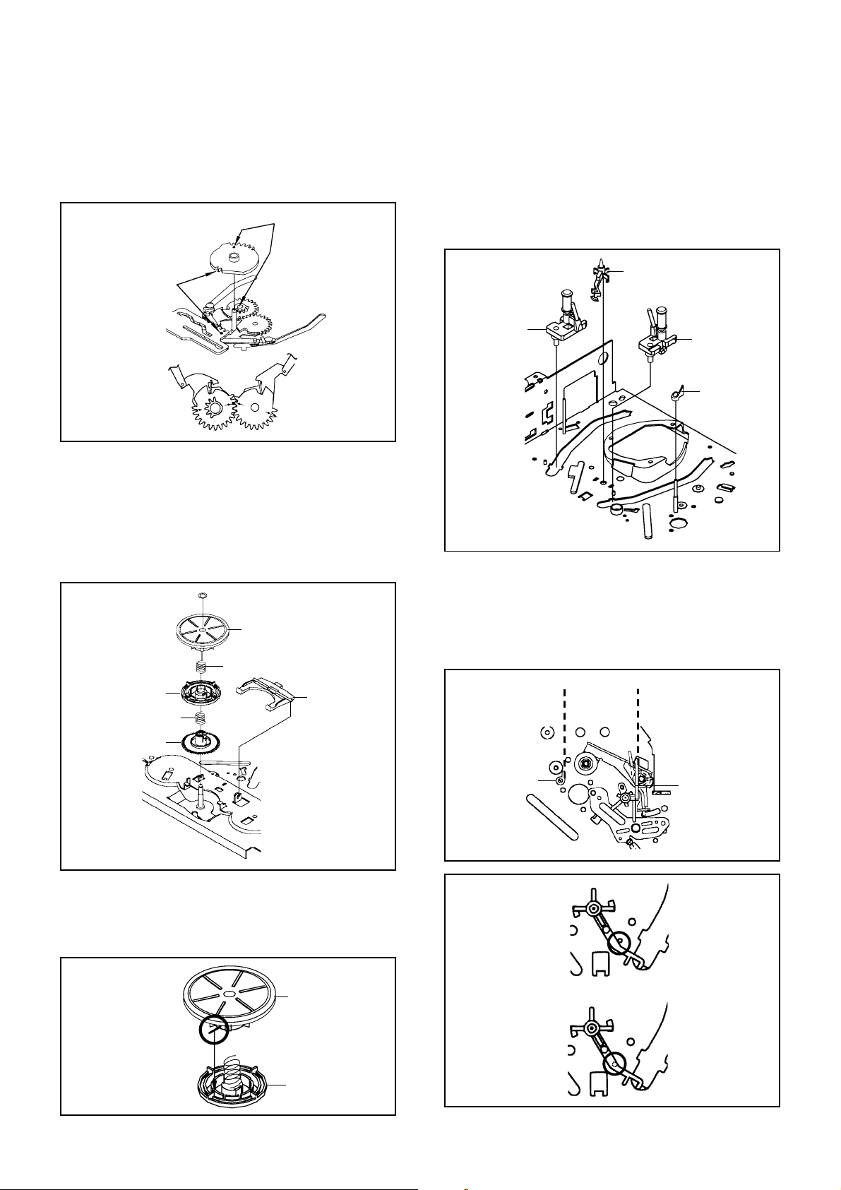
2-8: T BRAKE ARM/T BRAKE BAND (Refer to Fig. 2-8-A)
Remove the T Brake Spring.
1.
Turn the T Brake Arm clockwise and bend the hook
2.
section to remove it.
Unlock the 2 supports 1 and remove the T Brake
3.
Band.
Idler Gear
Idler Arm Ass'y
S Reel
T Brake Band
Hook section
1
1
T Brake Arm
T Brake Spring
Fig. 2-8-A
NOTE
1. In case of the T Brake Band installation, install correctly
as Fig. 2-8-B.
[OK]
T Brake Band
[NG]
T Brake Band
T Brake Arm
T Brake Arm
(A) T Reel
1
(A)
1
Fig. 2-9-A
NOTE
1.2.In case of the S Reel and T Reel installation, check if
the correct parts are installed. (Refer to Fig. 2-9-B)
In case of the Idler Arm Ass'y installation, install
correctly as Fig. 2-9-C.
Fig. 2-8-B
2-9: S REEL/T REEL/IDLER ARM ASS'Y/IDLER GEAR
(Refer to Fig. 2-9-A)
Remove the S Reel and T Reel.
1.
Remove the 2 Polyslider Washers 1.
2.
Remove the Idler Arm Ass'y and Idler Gear.
3.
NOTE
Take care not to damage the gears of the S Reel and T
1.
Reel.
The Polyslider Washer may be remained on the back of
2.
the reel.
Take care not to damage the shaft.
3.
Do not touch the section "A" of S Reel and T Reel. (Use
4.
gloves.) (Refer to Fig. 2-9-A) Do not adhere the stains
on it.
When you install the reel, clean the shaft and grease it
5.
(MG-33). (If you do not grease, noise may be heard in
FF/REW mode.)
After installing the reel, adjust the height of the reel.
6.
(Refer to MECHANICAL ADJUSTMENT)
[OK]
[NG]
Clutch Gear
Clutch Gear
Big Hole
(S Reel)
Small Hole
(T Reel)
Fig. 2-9-B
Idler Arm Ass'y
Idler Arm Ass'y
Fig. 2-9-C
B2-3
Page 12
DISASSEMBLY INSTRUCTIONS
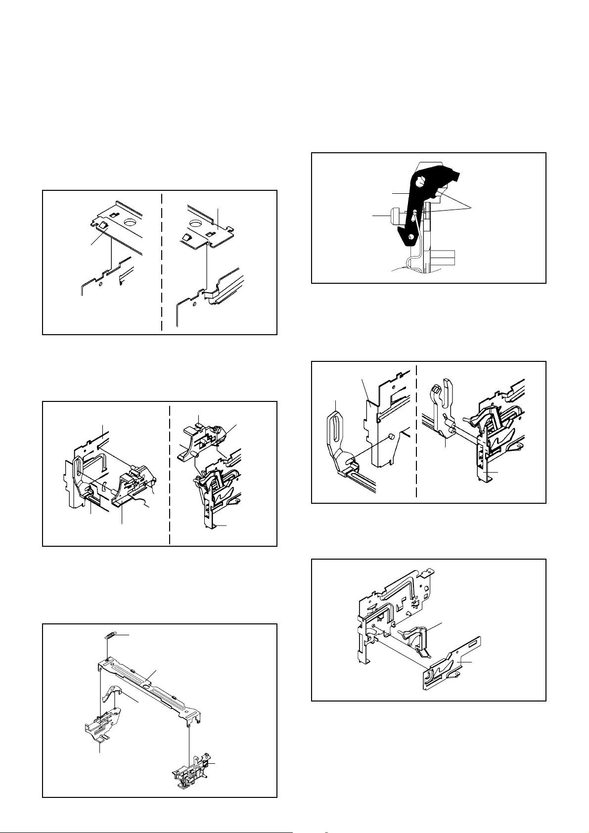
2-10: CASSETTE OPENER/PINCH ROLLER BLOCK/
P5 ARM ASS'Y (Refer to Fig. 2-10-A)
Unlock the support 1 and remove the Cassette
1.
Opener.
Remove the Pinch Roller Block and P5 Arm Ass'y.
2.
1
Cassette Opener
Pinch Roller Block
P5 Arm Ass'y
Main Chassis
Fig. 2-10-A
NOTE
Do not touch the Pinch Roller. (Use gloves.)
1.
In case of the Pinch Roller Block and the Pinch Roller
2.
Cam installation, install correctly as Fig. 2-10-B.
(3)(1)
2
2
(2)
1
• Screw Torque: 5 ± 0.5kgf•cm (Screw 1)
• Screw Torque: 4 ± 0.5kgf•cm (Screw 2)
Spring Position
2
A/C Head
A/C Head Spring
A/C Head Base
Fig. 2-11-A
Fig. 2-11-B
2-12: FE HEAD (RECORDER ONLY) (Refer to Fig. 2-12)
Remove the screw 1.
1.
Remove the FE Head.
2.
Pinch Roller Block
P5 Arm Ass'y
Can be seen the hole of the
Main Cam.
Can be seen the hole of
the Pinch Roller Cam.
Fig. 2-10-B
2-11: A/C HEAD (Refer to Fig. 2-11-A)
Remove the screw 1.
1.
Remove the A/C Head Base.
2.
Remove the 3 screws 2.
3.
Remove the A/C Head and A/C Head Spring.
4.
NOTE
1.
Do not touch the A/C Head. (Use gloves.)
2.
When you install the A/C Head Spring, install as shown
in Fig. 2-11-B.
3.
When you install the A/C Head, tighten the screw (1)
first, then tighten the screw (2), finally tighten the screw
(3).
1
FE Head
• Screw Torque: 4 ± 0.5kgf•cm
• The FE Head is not installed on the Video Cassette Player.
Fig. 2-12
B2-4
Page 13
DISASSEMBLY INSTRUCTIONS
2-13:AHC ASS'Y/CYLINDER UNIT ASS'Y
(Refer to Fig. 2-13)
Unlock the support 1 and remove the AHC Ass'y.
1.
Disconnect the following connector:
2.
(CD2001)
Remove the 3 screws 2.
3.
Remove the Cylinder Unit Ass'y.
4.
NOTE
When you install the Cylinder Unit Ass'y, tighten the
1.
screws from (1) to (3) in order while pulling the Ass'y
toward the left front direction.
Cylinder Unit Ass'y
1
(3)
(2)
(1)
• Screw Torque: 3 ± 0.5kgf•cm
2
2-14: CAPSTAN DD UNIT (Refer to Fig. 2-14)
Remove the Capstan Belt.
1.
Remove the 3 screws 1.
2.
Remove the Capstan DD Unit.
3.
2
2
AHC Ass'y
Fig. 2-13
2-15:
MAIN CAM/PINCH ROLLER CAM/JOINT GEAR
(Refer to Fig. 2-15-A)
Remove the E-Ring 1, then remove the Main Cam.
1.
Remove the E-Ring 2, then remove the Pinch Roller
2.
Cam and Joint Gear.
1
Main Cam
2
Pinch Roller Cam
Joint Gear
Fig. 2-15-A
NOTE
In case of the Pinch Roller Cam and Main Cam
1.
installation, install them as the circled section of Fig. 215-B so that the each markers are met. (Refer to Fig.
2-15-B)
Pinch Roller Cam
Marker
Main Cam
• Screw Torque: 4 ± 0.5kgf•cm
Capstan Belt
Capstan DD Unit
Fig. 2-15-B
2-16: LOADING GEAR S/T ASS'Y (Refer to Fig. 2-16-A)
1.2.Remove the E-Ring 1 and remove the Main Loading
Gear.
Remove the Main Rod, Tension Lever, Loading Arm S
Ass'y and Loading Arm T Ass'y.
1
1
1
1
Fig. 2-14
Main Rod
Tension Lever
Main Loading Gear
Loading Arm T Ass'y
Loading Arm S Ass'y
Fig. 2-18-A
B2-5
Page 14
DISASSEMBLY INSTRUCTIONS
NOTE
When you install the Loading Arm S Ass'y, Loading Arm
1.
T Ass'y and Main Loading Gear, align each marker.
(Refer to Fig. 2-16-B)
Marker
CASSETTE GUIDE POST/INCLINED BASE S/T
2-18:
UNIT/P4 CAP (Refer to Fig. 2-18-A)
Remove the P4 Cap.
1.
Unlock the support 1 and remove the Cassette Guide
2.
Post.
Remove the Inclined Base S Unit and Inclined Base T
3.
Unit.
Main Loading Gear
Marker
Loading Arm T Ass'y
2-17:
CLUTCH ASS'Y/RING SPRING/CLUTCH LEVER/
Loading Arm S Ass'y
CLUTCH GEAR (Refer to Fig. 2-17-A)
Remove the Polyslider Washer 1.
1.
Remove the Clutch Ass'y and Ring Spring.
2.
Remove the Clutch Lever.
3.
Remove the Coupling Gear, Coupling Spring and
4.
Clutch Gear.
1
Clutch Ass'y
Ring Spring
Coupling Gear
Coupling Spring
Clutch Lever
Fig. 2-16-B
Cassette Guide Post
Inclined Base T
Unit
P4 Cap
Inclined Base S
Unit
1
Fig. 2-18-A
NOTE
Do not touch the roller of Guide Roller.
1.
In case of the P4 Cap installation, install it with parallel
2.
for "A" and "B" of Fig. 2-18-B.
In case of the Cassette Guide Post installation, install
3.
correctly as the circled section of Fig. 2-18-C.
"A"
"B"
Clutch Gear
Fig. 2-17-A
NOTE
In case of the Clutch Ass'y installation, install it with
1.
inserting the spring of the Clutch Ass'y into the dent of
the Coupling Gear. (Refer to Fig. 2-17-B)
Clutch Ass'y
Coupling Gear
Fig. 2-17-B
B2-6
P4 Cap
[OK]
Cassette Guide Post
[NG]
Cassette Guide Post
Cassette Opener
Fig. 2-18-B
Fig. 2-18-C
Page 15
DISASSEMBLY INSTRUCTIONS
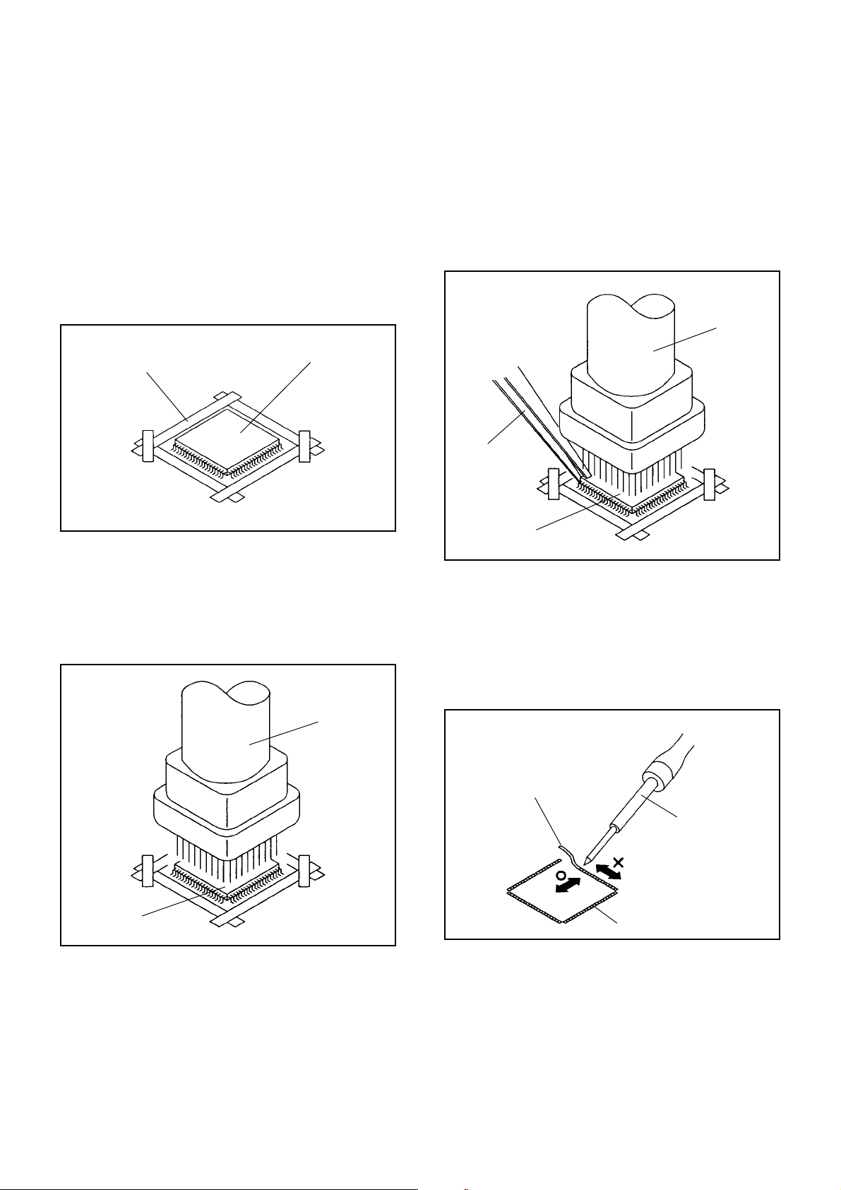
3.
REMOVAL AND INSTALLATION OF
FLAT PACKAGE IC
REMOVAL
Put the Masking Tape (cotton tape) around the Flat
1.
Package IC to protect other parts from any damage.
(Refer to Fig. 3-1.)
NOTE
Masking is carried out on all the parts located within
10 mm distance from IC leads.
When IC starts moving back and forth easily after
3.
desoldering completely, pickup the corner of the IC using
a tweezers and remove the IC by moving with the IC
desoldering machine. (Refer to Fig. 3-3.)
NOTE
Some ICs on the PCB are affixed with glue, so be
careful not to break or damage the foil of each IC
leads or solder lands under the IC when removing it.
Blower type IC
desoldering
machine
Masking Tape
(Cotton Tape)
Heat the IC leads using a blower type IC desoldering
2.
IC
machine. (Refer to Fig. 3-2.)
NOTE
Do not add the rotating and the back and forth
directions force on the IC, until IC can move back and
forth easily after desoldering the IC leads completely.
Blower type IC
desoldering machine
Fig. 3-1
Tweezers
IC
Fig. 3-3
Peel off the Masking Tape.4.
Absorb the solder left on the pattern using the Braided
5.
Shield Wire. (Refer to Fig. 3-4.)
NOTE
Do not move the Braided Shield Wire in the vertical
direction towards the IC pattern.
Braided Shield Wire
Soldering Iron
IC
Fig. 3-2
IC pattern
Fig. 3-4
B3-1
Page 16

DISASSEMBLY INSTRUCTIONS
INSTALLATION
Take care of the polarity of new IC and then install the
1.
new IC fitting on the printed circuit pattern. Then solder
each lead on the diagonal positions of IC temporarily.
(Refer to Fig. 3-5.)
Soldering Iron
Solder temporarily
Solder temporarily
Fig. 3-5
Supply the solder from the upper position of IC leads
2.
sliding to the lower position of the IC leads.
(Refer to Fig. 3-6.)
When bridge-soldering between terminals and/or the
4.
soldering amount are not enough, resolder using a Thintip Soldering Iron. (Refer to Fig. 3-8.)
Thin-tip Soldering Iron
IC
Fig. 3-8
Finally, confirm the soldering status on four sides of the
5.
IC using a magnifying glass.
Confirm that no abnormality is found on the soldering
position and installation position of the parts around the
IC. If some abnormality is found, correct by resoldering.
NOTE
When the IC leads are bent during soldering and/or
repairing, do not repair the bending of leads. If the
bending of leads are repaired, the pattern may be
damaged. So, be always sure to replace the IC in this
case.
Soldering IronSolder
IC
Absorb the solder left on the lead using the Braided
3.
Supply soldering
from upper position
to lower position
Shield Wire. (Refer to Fig. 3-7.)
NOTE
Do not absorb the solder to excess.
Soldering Iron
IC
Braided Shield Wire
Fig. 3-6
Fig. 3-7
B3-2
Page 17

A
A/C
ACC
AE
AFC
AFT
AFT DET
AGC
AMP
ANT
A.PB
APC
ASS'Y
AT
AUTO
A/V
B
BGP
BOT
BPF
BRAKE SOL
BUFF
B/W
C
C
CASE
CAP
CARR
CH
CLK
CLOCK (SY-SE)
COMB
CONV
CPM
CTL
CYL
CYL-M
CYL SENS
D
DATA (SY-CE)
dB
DC
DD Unit
DEMOD
DET
DEV
E
E
EF
EMPH
ENC
ENV
EOT
EQ
EXT
F
F
FBC
FE
FF
FG
FL SW
FM
FSC
FWD
G
GEN
GND
H
H.P.F
KEY TO ABBREVIATIONS
:
Audio/Control
:
Automatic Color Control
:
Audio Erase
:
Automatic Frequency Control
:
Automatic Fine Tuning
:
Automatic Fine Tuning Detect
:
Automatic Gain Control
:
Amplifier
:
Antenna
:
Audio Playback
:
Automatic Phase Control
:
Assembly
:
All Time
:
Automatic
:
Audio/Video
:
Burst Gate Pulse
:
Beginning of Tape
:
Bandpass Filter
:
Brake Solenoid
:
Buffer
:
Black and White
:
Capacitance, Collector
:
Cassette
:
Capstan
:
Carrier
:
Channel
:
Clock
:
Clock (Syscon to Servo)
:
Combination, Comb Filter
:
Converter
:
Capstan Motor
:
Control
:
Cylinder
:
Cylinder-Motor
:
Cylinder-Sensor
:
Data (Syscon to Servo)
:
Decibel
:
Direct Current
:
Direct Drive Motor Unit
:
Demodulator
:
Detector
:
Deviation
:
Emitter
:
Emitter Follower
:
Emphasis
:
Encoder
:
Envelope
:
End of Tape
:
Equalizer
:
External
:
Fuse
:
Feed Back Clamp
:
Full Erase
:
Fast Forward, Flipflop
:
Frequency Generator
:
Front Loading Switch
:
Frequency Modulation
:
Frequency Sub Carrier
:
Forward
:
Generator
:
Ground
:
High Pass Filter
H.SW
Hz
I
IC
IF
IND
INV
K
KIL
L
L
LED
LIMIT AMP
LM, LDM
LP
L.P.F
LUMI.
M
M
MAX
MINI
MIX
MM
MOD
MPX
MS SW
N
NC
NR
O
OSC
OPE
P
PB
PB CTL
PB-C
PB-Y
PCB
P. CON
PD
PG
P-P
R
R
REC
REC-C
REC-Y
REEL BRK
REEL S
REF
REG
REW
REV, RVS
RF
RMC
RY
S
S. CLK
S. COM
S. DATA
SEG
SEL
SENS
SER
SI
SIF
SO
SOL
SP
STB
SW
:
Head Switch
:
Hertz
:
Integrated Circuit
:
Intermediate Frequency
:
Indicator
:
Inverter
:
Killer
:
Left
:
Light Emitting Diode
:
Limiter Amplifier
:
Loading Motor
:
Long Play
:
Low Pass Filter
:
Luminance
:
Motor
:
Maximum
:
Minimum
:
Mixer, mixing
:
Monostable Multivibrator
:
Modulator, Modulation
:
Multiplexer, Multiplex
:
Mecha State Switch
:
Non Connection
:
Noise Reduction
:
Oscillator
:
Operation
:
Playback
:
Playback Control
:
Playback-Chrominance
:
Playback-Luminance
:
Printed Circuit Board
:
Power Control
:
Phase Detector
:
Pulse Generator
:
Peak-to Peak
:
Right
:
Recording
:
Recording-Chrominance
:
Recording-Luminance
:
Reel Brake
:
Reel Sensor
:
Reference
:
Regulated, Regulator
:
Rewind
:
Reverse
:
Radio Frequency
:
Remote Control
:
Relay
:
Serial Clock
:
Sensor Common
:
Serial Data
:
Segment
:
Select, Selector
:
Sensor
:
Search Mode
:
Serial Input
:
Sound Intermediate Frequency
:
Serial Output
:
Solenoid
:
Standard Play
:
Serial Strobe
:
Switch
C1-1
Page 18

S
SYNC
SYNC SEP
T
TR
TRAC
TRICK PB
TP
U
UNREG
V
V
VCO
VIF
VP
V.PB
VR
V.REC
VSF
VSR
VSS
V-SYNC
VT
X
X'TAL
Y
Y/C
KEY TO ABBREVIATIONS
:
Synchronization
:
Sync Separator, Separation
:
Transistor
:
Tracking
:
Trick Playback
:
Test Point
:
Unregulated
:
Volt
:
Voltage Controlled Oscillator
:
Video Intermediate Frequency
:
Vertical Pulse, Voltage Display
:
Video Playback
:
Variable Resistor
:
Video Recording
:
Visual Search Fast Forward
:
Visual Search Rewind
:
Voltage Super Source
:
Vertical-Synchronization
:
Voltage Tuning
:
Crystal
:
Luminance/Chrominance
C1-2
Page 19

SERVICE MODE LIST
This unit provided with the following SERVICE MODES so you can repair, examine and adjust easily.
Method Operations
Press the ATR button on the
remote control for more than
2 seconds during PLAY.
Make the short circuit between
the test point of SERVICE and
the GND.
Adjusting of the Tracking to the center position.
Refer to the "MECHANICAL ADJUSTMENT" (GUIDE ROLLER) and "ELECTRICAL
ADJUSTMENT" (PG SHIFTER).
The EOT/BOT/Reel sensor do not work at this moment.
Refer to the "PREPARATION FOR SERVICING"
C2-1
Page 20

PREVENTIVE CHECKS AND SERVICE INTERVALS
The following standard table depends on environmental conditions and usage. Unless maintenance is properly
carried out, the following service intervals may be quite shortened as harmful effects may be had on other parts.
Also, long term storage or misuse may cause transformation and aging of rubber parts.
Time
Parts Name
Audio Control Head
Full Erase Head
(Recorder only)
Capstan Belt
Pinch Roller
Capstan DD Unit
Loading Motor
Tension Band
Capstan Shaft
Tape Running
Guide Post
Cylinder Unit
: Clean
: Replace
500
hours
1,000
hours
CLEANING
NOTE
After cleaning the heads with isopropyl alcohol, do not
run a tape until the heads dry completely. If the heads
are not completely dry and alcohol gets on the tape,
damage may occur.
1. AUDIO CONTROL HEAD
Clean the Audio Control Head with the cotton stick
soaked by alcohol. Clean the full erase head in the
same manner. (Refer to the figure below.)
1,500
hours
2,000
hours
2. TAPE RUNNING SYSTEM
When cleaning the tape transport system, use the
gauze moistened with isopropyl alcohol.
3. CYLINDER
Wrap a piece of chamois around your finger. Dip it in
isopropyl alcohol. Hold it to the cylinder head softly.
Turn the cylinder head counterclockwise to clean it (in
the direction of the arrow). (Refer to the figure below.)
NOTE
Do not exert force against the cylinder head. Do not move
the chamois upward or downward on the head.
Use the chamois one by one.
3,000
hours
Notes
Clean those parts in
contact with the tape.
Clean the rubber, and parts
which the rubber touches.
Replace when rolling
becomes abnormal.
Clean the Head
Audio Control Head
Cylinder Head
C3-1
Page 21

SERVICING FIXTURES AND TOOLS
(For 2 heads model)
VHS Alignment Tape
JG001
JG001A
JG001Q
JG001T
(VN S-LI6 )
2
2
(VN S-CO1 )
2
(VN S-LI6 H)
(VN S-X6 )
3
2
Screwdriver
JG154 Cable
(For 4 heads model)
3
3
3
VHS Alignment Tape
JG001B
JG001I
JG001P
JG001S
1
(VN S-LI6 )
(VN S-CO1 )
1
1
(VN S-LI6 H)
1
(VN S-X6 )
3
3
3
3
JG002B
JG002E
JG002F
JG024AJG022 Master PlaneJG153 X Value Adjustment
Adapter
Dial Torque Gauge
(10~90gf•cm)
(60~600gf•cm)
Reel Disk Height
Adjustment Jig
JG005 Post Adjustment
Screwdriver
Part No. SV-TG0-030-000
(small)
JG100A Torque Tape
(VHT-063)
Tentelometer
Ref. No.
JG001
JG001A
JG001Q
JG001T
JG001B
JG001I
JG001P
JG001S
JG002B
JG002E
JG002F
JG005
JG153
JG022
JG024A
JG100A
JG154
Part No.
APJG001000
APJG001A00
APJG001Q00
APJG001T00
APJG001B00
APJG001I00
APJG001P00
APJG001S00
APJG002B00
APJG002E00
APJG002F00
APJG005000
APJG153000
APJG022000
APJG024A00
APJG100A00
APJG154000
Parts Name
VHS Alignment Tape (For 2 heads model)
VHS Alignment Tape (For 2 heads model)
VHS Alignment Tape (For 2 heads model)
VHS Alignment Tape (For 2 heads model)
VHS Alignment Tape (For 4 heads model)
VHS Alignment Tape (For 4 heads model)
VHS Alignment Tape (For 4 heads model)
VHS Alignment Tape (For 4 heads model)
Adapter
Dial Torque Gauge (10~90gf•cm)
Dial Torque Gauge (60~600gf•cm)
Post Adjustment Screwdriver
X Value Adjustment Screwdriver
Master Plane
Reel Disk Height Adjustment Jig
Torque Tape (VHT-063)
Cable
PREPARATION FOR SERVICING
Remarks
Monoscope, 6KHz
Color Bar, 1KHz
Hi-Fi Audio
X Value Adjustment
Monoscope, 6KHz
Color Bar, 1KHz
Hi-Fi Audio
X Value Adjustment
VSR Torque, Brake Torque (S Reel/T Reel Ass'y)
Brake Torque (T Reel Ass'y)
VSR Torque, Brake Torque (S Reel)
Guide Roller Adjustment
X Value Adjustment
Reel Disk Height Adjustment
Reel Disk Height Adjustment
Playback Torque, Back Tension Torque During Playback
Used to connect the test point of SERVICE and GROUND
Short circuit between TP1001 and Ground with the cable JG154.
1.
(Refer to MAJOR COMPONENTS LOCATION GUIDE)
The EOT, BOT and Reel Sensor do not work at this moment.
At that time, the STOP/EJECT button is available to insert and eject the Cassette Tape.
C4-1
Page 22

MECHANICAL ADJUSTMENTS
1. CONFIRMATION AND ADJUSTMENT
Read the following NOTES before starting work.
••Place an object which weighs between 450g~500g on
the Cassette Tape to keep it steady when you want to
make the tape run without the Cassette Holder. (Do not
place an object which weighs over 500g.)
When you activate the deck without the Cassette
Holder, short circuit between TP1001 and GND. (Refer
to ELECTRICAL ADJUSTMENT PARTS LOCATION
GUIDE) In this condition the BOT/EOT/Reel Sensor will
not function.
CONFIRMATION AND ADJUSTMENT OF REEL
1-1:
DISK HEIGHT
1.
Turn on the power and set to the STOP mode.
2.
Set the master plane (JG022) and reel disk height
adjustment jig (JG024A) on the mechanism framework,
taking care not to scratch the drum, as shown in Fig. 1-
1-A.
3.
While turning the reel and confirm the following points.
Check if the surface "A" of reel disk is lower than the
surface "B" of reel disk height adjustment jig (JG024A)
and is higher than the surface "C". If it is not passed,
place the height adjustment washers and adjust to
10(+2, -0)mm.
4.
Adjust the other reel in the same way.
1-2: CONFIRMATION AND ADJUSTMENT OF TENSION
POST POSITION
1.
Set to the PLAY mode.
2.
Adjust the adjusting parts for the Tension Arm position
so that the Tension Arm top is within the standard line of
Main Chassis.
3.
While turning the S Reel clockwise, confirm that the
edge of the Tension Arm is located in the position
described above.
Standard line of Main Chassis
Tension Arm
0.5mm (Adjusting range)
Fig. 1-2-A
Adjusting parts for the
Tension Arm position
Tension Band
Master Plane (JG022)
10(+0.2, -0)mm
Master Plane (JG022)
Height Adjustment
Washer
2.6x4.7xT0.13
2.6X4.7xT0.25
Reel Disk Height Adjustment Jig
(JG024A)
Reel Disk Height
Reel Disk
Adjustment Jig
(JG024A)
(B)
(A)
Fig. 1-1-A
(C)
Fig. 1-1-B
The Tension Arm top will
move to the inside direction
of the Main Chassis.
Bend
The Tension Arm top will
move to the outside direction
of the Main Chassis.
Fig. 1-2-B
1-3: CONFIRMATION OF PLAYBACK TORQUE AND
BACK TENSION TORQUE DURING PLAYBACK
Load a video tape (T-120) recorded in standard speed
1.
mode. Set the unit to the PLAY mode.
Install the tentelometer as shown in Fig. 1-3. Confirm that
2.
the meter indicates 20 ± 2gf in the beginning of playback.
• USING A CASSETTE TYPE TORQUE TAPE (JG100A)
1.
After confirmation and adjustment of Tension Post
position (Refer to item 1-2), load the cassette type
torque tape (JG100A) and set to the PLAY mode.
2.
Confirm that the right meter of the torque tape indicates
50~90gf•cm during playback in SP mode.
3.
Confirm that the left meter of the torque tape indicates
25~40gf•cm during playback in SP mode.
Tentelometer
Video Tape
P1 Post
Guide Roller
Fig. 1-3
D1-1
Page 23

MECHANICAL ADJUSTMENTS
1-4: CONFIRMATION OF VSR TORQUE
Install the Torque Gauge (JG002F) and Adapter (JG002B)
1.
on the S Reel. Set to the Picture Search (Rewind) mode.
(Refer to Fig.1-4-B)
Then, confirm that it indicates 120~180gf•cm.
2.
NOTE
Install the Torque Gauge on the reel disk firmly. Press the
REW button to turn the reel disk.
1-5: CONFIRMATION OF REEL BRAKE TORQUE
(S Reel Brake) (Refer to Fig. 1-4-B)
Once set to the Fast Forward mode then set to the Stop
1.
mode. While, unplug the AC cord when the Pinch Roller
Block is on the position of Fig. 1-4-A.
Move the Idler Ass'y from the S Reel.
2.
Install the Torque Gauge (JG002F) and Adapter
3.
(JG002B) on the S Reel. Turn the Torque Gauge
(JG002F) clockwise.
Then, confirm that it indicates 60~100gf•cm.
4.
(T Reel Brake) (Refer to Fig. 1-4-B)
Once set to the Fast Forward mode then set to the Stop
1.
mode. While, unplug the AC cord when the Pinch Roller
Block is on the position of Fig. 1-4-A.
Move the Idler Ass'y from the T Reel.
2.
Install the Torque Gauge (JG002E) and Adapter
3.
(JG002B) on the T reel. Turn the Torque Gauge
(JG002E) counterclockwise.
Then, confirm that it indicates 30~50gf•cm.
4.
The position at FF mode.
Pinch Roller Block
Stop at this position.
Cassette
The position at
STOP mode.
Capstan DD Unit
Cassette Holder Ass'y
Opener
Fig. 1-4-A
NOTE
If the torque is out of the range, replace the following
parts.
Check item
1-4
1-5
S Reel side:
Replacement Part
Idler Ass'y/Clutch Ass'y
S Reel/Tension Band/Tension
Connect/Tension Arm Ass'y
T Reel side:
T Reel/T Brake Band//T Brake
Spring/T Brake Arm
2. CONFIRMATION AND ADJUSTMENT
OF TAPE RUNNING MECHANISM
Tape Running Mechanism is adjusted precisely at the
factory. Adjustment is not necessary as usual. When you
replace the parts of the tape running mechanism because
of long term usage or failure, the confirmation and
adjustment are necessary.
2-1: GUIDE ROLLER
Playback the VHS Alignment Tape (JG001 or JG001B).
1.
(Refer to SERVICING FIXTURE AND TOOLS)
Connect CH-1 of the oscilloscope to TP4001 (Envelope)
2.
and CH-2 to TP1002 (SW Pulse).
Press and hold the Tracking-Auto button on the remote
3.
control more than 2 seconds to set tracking to center.
Trigger with SW Pulse and observe the envelope. (Refer
4.
to Fig. 2-1-A)
When observing the envelope, adjust the Adjusting
5.
Driver (JG005) slightly until the envelope will be flat.
Even if you press the Tracking Button, adjust so that
flatness is not moved so much.
Adjust so that the A : B ratio is better than 3 : 2 as shown
6.
in Fig. 2-1-B, even if you press the Tracking Button to
move the envelope (The envelope waveform will begin to
decrease when you press the Tracking Button).
Adjust the PG shifter during playback.
7.
(Refer to the ELECTRICAL ADJUSTMENTS)
NOTE
After adjustment, confirm and adjust A/C head.
(Refer to item 2-2)
Torque Gauge/Adapter
(JG002F/JG002B)
S Reel
Torque Gauge/Adapter
(JG002E/JG002B)
T Reel
Fig. 1-4-B
D1-2
CH-1
Envelope
(TP4001)
CH-1
Track
CH-2
SW Pulse (TP1002)
Entrance Exit
Max
A
A : B ≥ 3 : 2
B
CH-2
Track
Fig. 2-1-A
Max
Fig. 2-1-B
Page 24

MECHANICAL ADJUSTMENTS
CONFIRMATION AND ADJUSTMENT OF AUDIO/
CONTROL HEAD
When the Tape Running Mechanism does not work well,
adjust the following items.
1.
Playback the VHS Alignment Tape (JG001 or JG001B).
(Refer to SERVICING FIXTURE AND TOOLS)
2.
Confirm that the reflected picture of stamp mark is
appeared on the tape prior to P4 Post as shown in Fig.
2-2-A.
a)
When the reflected picture is distorted, turn the screw
1 clockwise until the distortion is disappeared.
b)
When the reflected picture is not distorted, turn the
screw 1 counterclockwise until little distortion is
appeared, then adjust the a).
3.
Turn the screw 2 to set the audio level to maximum.
4.
Confirm that the bottom of the Audio/ Control Head and
the bottom of the tape is shown in Fig. 2-2-C.
c)
When the height is not correct, turn the screw 3 to
adjust the height. Then, adjust the 1~3 again.
Audio/Control Head
Reflected picture of
Stamp Mark
P4 Post
2-3:2-2:
TAPE RUNNING ADJUSTMENT
(X VALUE ADJUSTMENT)
Confirm and adjust the height of the Reel Disk.
1.
(Refer to item 1-1)
Confirm and adjust the position of the Tension Post.
2.
(Refer to item 1-2)
Adjust the Guide Roller. (Refer to item 2-1)
3.
Confirm and adjust the Audio/Control Head.
4.
(Refer to item 2-2)
Connect CH-1 of the oscilloscope to TP4001, CH-2 to
5.
TP1002 and CH-3 to HOT side of Audio Out Jack.
Playback the VHS Alignment Tape (JG001S or
6.
JG001T). (Refer to SERVICING FIXTURE AND TOOLS)
Press and hold the Tracking-Auto button on the remote
7.
control more than 2 seconds to set tracking to center.
Set the X Value adjustment driver (JG153) to the 4 of
8.
Fig. 2-2-B. Adjust X value so that the envelope waveform
output becomes maximum. Check if the relation between
Audio and Envelope waveform becomes (1) or (2) of Fig.
2-3.
Envelope
(1)
CH-3
Audio
(2)
Audio/Control Head
3
2
Audio/Control Head
Tape
Stamp Mark
1
4
Fig. 2-2-A
Fig. 2-2-B
0.25±0.05mm
Fig. 2-2-C
Fig. 2-3
2-4: CONFIRM HI-FI AUDIO (Hi-Fi model only)
Connect CH-1 of the oscilloscope to TP1002 and CH-2 to
1.
the Hi-Fi Audio Out Jack.
Playback the VHS Alignment Tape (JG001P or JG001Q).
2.
(Refer to SERVICING FIXTURE AND TOOLS)
Press and hold the Tracking-Auto button on the remote
3.
control more than 2 seconds to set tracking to center.
Press the Tracking Up button and count number of steps
4.
which the audio output is changed from Hi-Fi (10KHz) to
MONO (6KHz).
Press and hold the Tracking-Auto button on the remote
5.
control more than 2 seconds to set tracking to center.
Press the Tracking Down button and count number of
6.
steps which the audio output is changed from Hi-Fi
(10KHz) to MONO (6KHz).
If the difference are more than 3 steps, set the X Value
7.
adjustment driver (JG153) to 4 of Fig. 2-2-B. Change the
X Value and adjust it so that the value becomes within 2
steps.
D1-3
Page 25

MECHANICAL ADJUSTMENTS
3. MECHANISM ADJUSTMENT PARTS LOCATION GUIDE
3
4
5
6
2
1
8910
1. Tension Connect
2. Tension Arm
3. Guide Roller
4. Audio/Control Head
5. X value adjustment driver hole
6.
P4 Post
7.
T Brake Spring
8.
T Reel
9.
S Reel
10.
Adjusting parts for the Tension Arm position
7
D1-4
Page 26

ELECTRICAL ADJUSTMENTS
Read and perform this adjustment when repairing the
circuits or replacing electrical parts or PCB assemblies.
1. BASIC ADJUSTMENT
CAUTION
When replacing IC's or transistors, use only specified
silicon grease (YG6260M).
(To prevent the damage to IC's and transistors.)
1-1:PG SHIFTER
CONDITIONS
MODE-PLAYBACK
Input Signal-Alignment Tape (JG001B)
INSTRUCTIONS
1.
Connect CH-1 on the oscilloscope to TP1002 and CH-2
to TP4201.
2.
Playback the alignment tape. (JG001B)
3.
Press and hold the Tracking-Auto button on the remote
control more than 2 seconds to set tracking to center.
4.
Adjust the VR1001 until the waveform of the oscilloscope
measures 6.5 ± 0.5(H) at both leading and trailing edges.
(Refer to Fig. 1-1-A, B)
6.5H
CH-2
CH-1
Fig. 1-1-A
CH-2
CH-1
6.5H
Fig. 1-1-B
D2-1
Page 27

ELECTRICAL ADJUSTMENTS
2. ELECTRICAL ADJUSTMENT PARTS LOCATION GUIDE
TP1001
J4205 J4203
T501
VR1001
TU6001
TP4001
TP1002
TP4201
J4201
SYSCON PCB
D2-2
Page 28

Y/C/AUDIO/CCD/HEAD AMP BLOCK DIAGRAM
X4001
100CT3R508
Q4012
BUFFER
CYL
FE HEAD
CP4001
1 EP/LP_CH2 (L)
2
EP/LP_COM
3
EP/LP_CH1(R)
4
SP_CH2(L)
5
SP_COM
SP-CH1(R)
6
7
8
9
CP4003
FE HEAD (HOT)
1
2
FE HEAD (GND)
Y/C/AUDIO/CCD/HEAD AMP IC
IC4001
LA71201M-N-MPB
67
66
65
72
73
74
9
7
8
6
L
H
H
L
REC AMP
AUTO BIAS
H.SW
H
H.AMP
SW
L
H.SW
PB.EE
50
VX01
P
R
FM
AGC
DELAY
PB
FM-EQ
PB
PHASE-EQ
EQ
AMP
49
TIMMING
AGC
AMP
R
41
PULL
REC
FM-EQ
KIL
C-LPF
GCA
P
DOUBLE
LIM
DRIVER
B-UP
AMP
ACC
AMP
MUTE
FM
MOD
P
R
OUT
P
KIL
B.D.
FM
DEM
ALC
DET
39
CCD
Main
CONV
R
WC
DC
CLAMP
3.58M
BPF2
3.58M
BPF1
PB
AMP
LINE
AMP
LPF
ALC
37
NL
EMPHA
V/I
CONV
SUB
LPF
Q4010
BUFFER
Y-LPF
V-AGC
DETAL
ENH
P
R
P
Y/C MIX
SYNC
SEP
R
YNR/
COMB
N.L.
DEEM
NC1
P
R
R
P
SERIAL
DECODER
CLAMP
CLAMP
H.AMP SW/
AUDIO MUTE
1/2
RF SW IN
FBC
ENV DET
Chara
INS.
6dB
VCA
C ROT
CONP
OUT
55
54
53
22
21
36
58
57
59
60
24
26
34
Y/C_CS
IIC_DATA
IIC_CLK
H. AMP_SW
C. ROTARY
H. SW
AUDIO_MUTE-H
ENV. DET
COMP
DUMMY_V. SYNC
OSD_V
SYSCON/SERVO
SYSCON/SERVO
HEAD
AUDIO
CONTROL
E-1
CP4002
6
AUDIO PB
5
AUDIO REC
4
CTL+
CTL-
3
2
AE HEAD(-)
AE HEAD(+)
1
COIL, BIAS OSC
T4001
5
6
4
Q4001, Q4002
AUDIO PB SW
11
Q4005
2
3
1
BIAS CTL
Q4006
BIAS OSC
Q4003
5 78 76
SW
3
4
P. CON + 5V
10
2
32
30
FSC
FRONT_V_IN
TUNER_V
TUNER_A
FRONT_A_IN_L
FROM_NORMAL_A
V.REC_ST-H
CTL+
CTL-
TUNER
SYSCON/SERVO
E-2
Page 29

POWER
MODE_VCC
AT+5.2V
DECK
P.CON+5V
POWER_FAIL
POWER_ON-H
P.CON+5V
AT+12.6V
CP1001
1
CAP_FG
2
CAP_VCO
VCC
3
4
CAP/M/F/R
I_LIMIT
5
8
LD/CY_VCO
9
CAP_CTL
10
LDM_CTL
11
CYL_FG/PG
12
CYL_CTL
Q1007
CENT SW
MS_SEN B
Q1004
BOT SENSOR
Q1008
2
1
3
4
EOT SENSOR
Q1006
2
1
3
4
REEL SENSOR
Q1002
2
1
MS_SEN A
Q1005
3
4
SYSTEM CONTROL/SERVO BLOCK DIAGRAM
SYSCON/TIMER/SERVO IC
IC1001 OEC0104B
CENT LED
61
7
MS SEN-A
6
MS SEN-B
REEL-T
87
EOT-H
12
BOT-H
3
89
POWER FAIL-H
64
POWER ON_H
40
CFG
DPG
39
CAP FWD
60
66
CAP LIMIT
CAP FULL21
CAP PWM25
63
CYL SPEED UP
38
DFG
65
LDM_CTL
P.OFF-L
FS/IIC CLK
IIC DATA
Y/C_CS
DUMMY V.SYNC
V.REC ST-H
C.ROTARY
A.MUTE
CV IN
CTL-H(-)
CTL-H(+)
H.AMP SW
COMP
ENV DET
C.SYNC
AFT S. CURVE
AUDIO OUT MUTE-L
VCR-H(TV/VCR)
CV OUT
TUNER-L
55
18
19
20
27
56
28
59
43
32
31
29
30
14
H.SW
24
54
11 AFT-S.CURVE
93
84
45
58
4FSC
IIC_CLK
IIC_DATA
Y/C_CS
DUMMY_V.SYNC
V.REC_ST-H
C.ROTARY
AUDIO.MUTE-H
OSD_V
CTLCTL+
H.AMP_SW
COMP
ENV.DET
H.SW
C.SYNC
IIC_CLK
IIC_DATA
A_OUT_MUTE-L
TV/VCR
VIDEO_OUT
TUNER-L
Y/C/AUDIO/CCD/
HEAD AMP
TUNER
E-3
OPERATION
REM_IN
KEY-B
KEY-A
1G/TV/VCR_LED
2G/T-REC_LED
3G/REC_LED
82
REM_IN
8
KEY-B
9
KEY-A
79
1G/TV/VCR LED
78
2G/T-REC LED
3G/REC LED77
TAB SW
OSD 1
OSC 2
RESET
80
72
73
16
X1001
CSTS1000MG96004-T2
IC1003
R3111N311A/C-TR
SYSTEM
1
RESET IC
SW1001
E-4
Page 30

SYSCON/SERVO
VIDEO_OUT
P. CON + 12V
RF-SW
SW6001
TUNER BLOCK DIAGRAM
REAR OUT JACK
J4201
2
Q4201
BUFFER
3
FRONT AV JACK
VIDEO
J4203
2
MONO AUDIO
J4205
2
TUNER_V
FRONT_V_IN
FSC
2
FRONT_A_IN-L
FROM_NORMAL_A
TUNER_A
TU6001
3
6
2
15
5
11
12 IIC_DATA
21
23
24
TV/VCR
IIC_CLK
AFT-S. CURVE
Y/C/AUDIO/CCD
HEAD AMP
SYSCON/SERVO
E-5
E-6
Page 31

OPERATION BLOCK DIAGRAM
CH UP
CH DOWN
STOP/EJECT
REC/OTR
FF/CUE
PLAY
REW/REV
T501
POWER
KEY-A
KEY-B
CP601
CP651
3
2
3
2
POWER BLOCK DIAGRAM
OS651
1
3
TV/VCR LED
D664
T_REC LED
D665
REC LED
D666
KEY-A
KEY-B
REM_IN
1G/TV/VCR_LED
2G/T-REC_LED
3G/REC_LED
SYSCON/SERVO
D505, D508,
D523, D528
F501
L501
5
2
4
Q503
SW
10
7
8
6
Q502
CONTROL
IC511
PHOTO
COUPLER
IC505
PHOTO
COUPLER
IC501
KIA431
VOLTAGE
CTL IC
3
+32V
P. CON +12V
Q506
P. CON
+5V SW
Q508
P. ON SW
P. CON + 5V
1
Q515
M-CON B+ SW
AT +5V[M-CON]
AT +12.6V
POWER_ON-H
SYSCON/SERVO
POWER_FAIL
E-7
AC IN
E-8
Page 32

PRINTED CIRCUIT BOARDS
SYSCON/OPERATION (INSERTED PARTS)
SOLDER SIDE
C4211
C6003_1
W154
W153
TU6001
W159
W143
VR1001
W813
C6010
W157
C4201
W844
R6010
R6004
J4203
L6002
Q4201
R4201
W816
SW6001
SW604_1
CP601_1
W158
W160
TP4201
SW603_1
C4209
R4213_1
W161
R604
Q1006
L6003
W803
W811
J4205_1
W863
TP4001
TP1002
J4201_3
SW605
W150
W116
SW607
W113
SW606_1
W131
CP4003
SW608
R1075
W815
R1043
R1076
C1023
W127
W115
SW1001
W114
W121
W136
R4045
W122
W096
TP1001
W119
W125
W139
W141
L4006
R658
L4005
C4063
W094
C4009
W081
W851
R4047
W039
L4001
W091
W089
W082
W103
W083
W107
CP4001
W071
W088
W087
W085
R1031
W109
R1073_1
C4065
C4062
X4001
C4070
C4013
W111
W110
D664
W074
W833
W090
C1021
R1074_1
W092
C4067
W077
W101
C4059
W824
W100
R4033
C4012
W835
C1038
C4048
R4020
C1020
C4058
C4030
D665
W075
W086
W095
W033
W084
D1001
W093
C4052
C4053
W078
C4049
C4027
R659
W079
W043
W042
C4051
C4046
R4053
W038
W029
C4050
L4004
C4031
Q4002
C4014
D666
W047
C4035
C4034
W037
W054
Q4001
W069
R660
X1001_1
C1006
W041
W053
W049
W801
C4045
C4010
W040
W067
C4025
C4002
W045
W051
Q4005
D663
R657
W838
W829
W061
W055
C4004
T4001
Q4006
W070
CP4002
W044
W048
W064
L4003
Q1002
L1001
W057
W066
W036
C1022
W056
W068
W065
W062
W052
W857
W828
W060
W059
W030
OS651
Q506
Q515
R1006
C1029
Q508
W845
W050
W808
W034
R1002
W012
W032
W031
R1010
R4004
W840
R530
W818
W027
W058
D1004
D1003
W003
D1002
W025
R1003
W028
R531
W023
R1022
R1038
L1002_1
R521
R509
W002
W001
W011
L505_1
W008
W017
W015
W013
CP1001
D1005
W005
Q1004
Q1005
R1016
W022
W021
C522
W019
W018
R548
C1001
C520
W020
W097
W026
W837
R502
SW660
L504_1
W852
W820
D501
D525
W016
IC511
IC501
C505_1
W809
C504
SW659
W006
C502
D520
D521
W010
R537
D507
W024
IC505
A_V_
RISK OF FIRE -REPLACE AS MARKED.
C514
D514
B501
R549
C518
D502
R511
W826
W841
Q502
R514
Q1008
C508
D508
D505
R547
D506
L501
1.6A125VOR250V
FH502
S502
B502
D511
F501
T501
W864
CP651_1
D512
Q503_2
R534
C509
C512_1
D528
S501
C519
R512
D523
FH501
CD501
.
F-1
F-2
Page 33

C529
R524
R1004
R516
R510
R518 R506
C515
PRINTED CIRCUIT BOARDS
SYSCON/OPERATION (CHIP MOUNTED PARTS)
SOLDER SIDE
R4006
C4020
R4016
C4021
R4014
C4028
C4029
R4003
R4024
C4037
R4019
R4018
R4021
C4033
R4017
C4036
C4054
C4074
C4044
R4034
R4035
R4022
C4032
21
Q4010
R4037
C1036
Q4011
IC4001
C4061
C4060
R4036
41
1
R4043
R4038
61
C4066
R4042
Q4012
R4012
R4041
C4015
C4019
C4016_1
C4064
R4039
R1009
Q1007
R4007
R4046
R1041
R4010
C4006
R1039
C4005
R4001
R4044
C4038
Q4003
R4023
R4025
C4057
R4002
R4011
C4069
R1007
C4204
C6014
R4205
R4210
R4202
R6005
R6006
C6009_1
C6002
C506
C534
C507
R527
R1087
R544
R1083
R1050
R1013
R519
R1061
C1019
R1070
C1013
C1032
R1017
R1015
R1014
C1034
C1016
R1072
C1040
R1030
R1065
R1053
R1026
R1025
R1040
C1055
R1048
R1052
R1055
C1015
51
R1054
R1033
31
IC1001
C1054
R1037
81
R1034
C1053
C1041
1
IC1003
C1017
R1049
R1045
R1051
R1044
R1046
R1047
R1042
R1066
R1062
R1058
R605
R607
R601
R602
R603
R4209
F-3
F-4
Page 34

ABC D E F GH
Y/C/AUDIO/CCD/HEAD AMP SCHEMATIC DIAGRAM
8
(SYSCON PCB)
8
7
6
FROM/TO CYL
CP4001
TOC-C09X-A1
5
9
8
7
6
SP-CH1 (R)
5
SP_COM
4
SP-CH2 (L)
3
EP/LP-CH1 (R)
2
EP/LP COM
1
EP/LP-CH2 (L)
4
3
FROM/TO HEAD AUDIO CONTROL
CP4002
IMSA-9604S-06Z13
6
5
4
3
2
1
2
TO FE HEAD
CP4003
TMC-T02X-E1
FE HEAD(GND)
2
FE HEAD(HOT)
1
1
FROM POWER
P.CON+5V
GND
AUDIO PB
AUDIO REC
CTL+
CTL-
AE HEAD(-)
AE HEAD(+)
COMP
ENV.DET
H.AMP_SW
22K
R4044
0.1 F
C4069
OUT
C4016_1
0.068 B
C4019
0.047 F
C4015
0.047 F
NC
NC
NC
P.CON+5V
TUNER_A C.SYNC
P.CON+5V DUMMY_V.SYNC
FRONT_A_IN-L P.CON+5V
P.CON+5V
V.REC_ST-H
CTL+
CTL-
AUDIO
PB SW
Q4001
KTC3198
AUDIO
PB SW
Q4002
KTC3198-AT
GND
HOT
(Y,GR}
NOTE:THIS SCHEMATIC DIAGRAM IS THE LATEST AT THE TIME
L4001
22uH 0305
476.3V KA
0.1 B
C4009
C4013
R4007
226.3V KA
6
5
47K
R4006
47K
COIL,BIAS OSC
T4001
1626009
1
2
34
C4004
C4014
226.3V KA
C4005
2206.3V YK
C4006
0
R4001
560
0
R4002
0.7 5
10K
0
0
R4003
0.7
0
5.2
5.3
10K
R4004
15 1/4W
SW
Q4003
KRA103RTK
C4002
C4012
0.022100V MKT
OF PRINTING AND SUBJECT TO CHANGE WITHOUT NOTICE
R4012
C4020
0.1 F
C4021
0.1 F
R4014
R4010
0.01 B
3.3K
0
L4003
100uH
0305
0
BIAS OSC
0
Q4006
KTC3203_Y
Y/C/AUDIO/CCD/HEAD AMP IC
BIAS CTL
Q4005
KTA1266
0
5.2
IC4001
LA71201M-N-MPB
5.2
R4011
22K
C4010
476.3V KA
5.6K
R4016
4.7K
0.015 B
COMP
2.1
KILL
616263646566676869
DET
0
HA
GND
2.9
CHROMA
DET
ACC
1.6
DET
1.8
1.9
1.8
5.0
HA VCC
1.8
1K
1.6
70717273747576777879
HA
0
PRE GND
1.8
1.8
1.8
0
A-GND
2.3
4.9
A-VCC
2.3
0
2.3
Vref
NC
2.3V
2.3 2.3 2.3 2.3 2.3 2.3
C4027
C4025
2206.3V YK
THE DC VOLTAGE AT EACH PART WAS
NOTE:
MEASURED WITH THE DIGITAL TESTER
DURING PLAYBACK
AUDIO
ENV
DET
HA SW
P
R
P
P
R
P
1
2
3
1 10111213141516
0.1 F
C4028
R4053
10K
336.3V KA
C4074
0.001 B
C.ROTARY
AUDIO_MUTE-H
R4046
R4045
12K 1/4W
C-ROT
MUTE
RF-SW
IN
H
L
H
L
ALC
ALC
DET
EQ
AMP
SP,LP
3
4
1/4W
8.2K
R4017
8.2K
R4018
R4019
330K
C4029
0.01 B
22K
C4070
C-GND
C4030
H.SW
R4047
PB,EE
R4020
Y/C_CS
IIC_CLK
IIC_DATA
P.CON+5V
C4063
DETAIL
ENH
EMPHA
LINE
AMP
MUTE
R4041
1.8K
4716V YK
150V KA
8.2K
C4064
0.022 B
2
X4001
100CT3R508
VX01
PB
REC
APC
APC
P
R
BGA
R
ACC
AMP
R
PP
ACC
DET
P
R
CLAMP
NL
NL
EMPHA
FM
MOD
R-EQ
NORMAL
TEST
REC
FM-EQ
FM
R
P
AGC
PHASE
AUTO
EQ
BIAS
fo-ADJ
R4023
4.725V KA
47uH
12K 1/4W
L4006
0.1 F
C4062
R4039
C-VCC
SERAIL
DECODER
RP
3.58M
BPF2
Main
B-UP
CONV
AMP
4.21M
BPF
Sub
CONV
LPF
VREF
REC
AMP
8809
2.3 2.3 0.8 4.8 1.1 1.1 1.4 2.0 0 2.6
820
R4022
0.0027 B
R4021
18K
C4034
C4033
+
R
P
C-LPF
PB,EE
REC:LP<EP
PB:EP
7
0
C4032
0.0012 B
150V KA
C4031
4
1016V KA
180 1/4W
FROM_NORMAL_A
4.9
BUFFER
Q4012
3.9
2SC2412K
3.3
3.3K
R4043
150V KA
150V KA
C4067
C4065
C4066
0.022 B
1.5K
R4042
NC
3.3 3.2
ALWAYS
LIM
SLD
PB-C
S-EQ
YNR/COMB
P
R
SOPB
5V
B
CNC
PB
AMP
B.D
P
3.58M
BPF1
R
N.L.
PB-C
DEEM
NC1
FM
SUB
DEM
LPF
MAIN
DE-EM
R
P
FM
AGC
Y-GND
FIL
BEFORE
P
320FH
VCO
P
AFTER
P
PHASE
EQ
Q-ADJ
R
REC
AFC
R
FM EQ
PB
BGA
BGA
Y-LPF
DOUBBLE
VHS
33K
150V KA
C4035
5.6K
R4024
V.ENV
3
TP4001
NC
CAUTION: DIGITAL TRANSISTOR
P.CON+5V
47uH
L4005
C4058
476.3V KA
C4059
0.1 F
R4038
680K
VDD 4Fsc
PLL
TIMMING OUT
AUTO-BIAS
DRIVER
CCD
CLAMP
VIDEO
AGC
1/2
FBC
R
Y/C
P
MIX
R
P
QV/QH
SYNC
SEP
V.SYNC
SEP
R
P
4.7K
MAIN
EMPHA
DET
FIL
17 18 192 20
2.6 0.2 2.8
NC
C4037
C4036
390P B
CLAMP
VCA
1
2
3
6DB
S
0.82.21.24.94.93.24.95.25.25.205.204.84.8 2.1 4.1
C4060
Y-VCC
R4025
0.1 F
C4038
FSC
7
0.01 B
2.2K 1/4W
R4034
82K
R4037
1K
4FSC
R4035
100K
TUNER_V
FRONT_V_IN
1
OSD_V
C4061
0.01 B
414243444546474849550515253545556575859660
CLOCK
0
40
VSS
1.6
OUT
0
VSS
3.2
IN
2.5
VCA
3.2
C4049
3.3
2.6
VCP
2.6
4.1
REG
4V
2.3
30 31 32 33 34 35 36 37 38 39
BAL
2.3
TC1
2.1
NC
NC
AGC
1.6
TC2
3.6
C4048
150V KA
150V KA
W801
1.8K
R4036
4.9
3.8
3.2
BUFFER
Q4010
2SA1037AK
1.6
BUFFER
Q4011
2SC2412K
2.20
C4052
150V KA
C4053
150V KA
C4054
0.1 F
C4050
0.2250V KA
C4051
226.3V KA
R4033
4.1
5.0
4.4
3.2
2.1
B
21 22 23 24 25 26 27 28 29
C4046
150V KA
L4004
22uH
FROM/TO TUNER
FSC
FRONT_V_IN
FRONT_A_IN-L
TUNER_V
TUNER_A
FROM_NORMAL_A
FROM/TO SYSCON/SERVO
4FSC
IIC_CLK
IIC_DATA
Y/C_CS
DUMMY_V.SYNC
V.REC_ST-H
C.ROTARY
AUDIO_MUTE-H
OSD_V
CTL-
CTL+
H.AMP_SW
COMP
ENV.DET
H.SW
C.SYNC
6
5
4
3
1006.3V KA
C4045
C4044
0.1 B
1.5K
C4057
10P CH
180P CH
2
PCB010
VMA224
1
AUDIO SIGNAL(PB)
AUDIO SIGNAL(REC)
TUNER VIDEO SIGNAL
RECORD COLOR SIGNAL
RECORD LUMINANCE SIGNAL
PLAYBACK COLOR SIGNAL
PLAYBACK LUMINANCE SIGNAL
ABC D E F GH
G-2G-1
Page 35

ABC D E F GH
FROM/TO POWER
POWER_FAIL
8
LED_VCC
POWER_ON-H
AT+5V[M-CON]
P.CON+5V
AT+5.2V
AT+12.6_V
GND
GND
GND
(S/S)
(MOTOR)
(LED)
7
C1001
D1003
1SS133
D1004
1SS133
22016V YK
L1002_1
22uH
R1003
3.3K 1/4W
W809
1SS133
D1005
12
R1009
R1010
10K 1/4W
5.1
0
R1007
R1006
47K 1/4W
8.2K
CAP_F/R
LDM_CTL
CYL_DRIVE
10K
CYL_PG
CYL_FG
LED_VCC
EOT SENSOR
Q1006
PNA2604M010R
CENT_LED
(LED_GND)
CAP_FG
CAP_LIMIT
CONTROL_IN
47K
R1042
TAB_SW
EOT
BOT
GND
REEL-T
REM_IN
CAP_FG
TV/VCR
REEL-T
POWER_FAIL
14
W851
R1058 2.2K
R1062 2.2K
0
NC
5.0
0
5.0
NC
NC
5.0
5.0
NC
4.2
0
4.9
NC
5.0
NC
5.0
NC
0.3
5.0
NC
0.7
NC
0.1
NC
5.0
NC
0
NC
SW1001
MXS01350MVP0
R1002
180 1/4W
FROM/TO DECK
CP1001
TMC-J12P-B2
CAP_FG
1
CAP_VCO
2
3
CAP/M/F/R
4
I_LIMIT
5
6
7
LD/CY_VCO
8
CAP_CTL
9
LDM_CTL
10
CYL_FG/PG
11
CYL_CTL
12
5.0
BOT SENSOR
Q1008
0
PNA2604M010R
KRC103RTK
R1004 8.2K
1.2
2
REEL SENSOR
34
Q1002 RPI-301
5.2
VCC
GND[M]
GND
CENT SW
Q1007
W808
D1001
LNA2702L010R
270
R1041
0
5.0
0
2.4
1
W845
0
6
5
4
3
2
5.0
1.4
MS_SEN B
Q1004
SG-233S
23
1
4
1.60.6
1
SYSTEM CONTROL/SERVO SCHEMATIC DIAGRAM
(SYSCON PCB)
22K
CAP_F/R
AUDIO_MUTE-H
A.MUTE
CAP FWD
VDD (60K=TEST)
CAP FULL
05.005.05.005.0
VIDEO H.SW
C1041
IC1003
R3111N311A/C
SYSTEM RESET IC
R1070
V.REC_ST-H
5.0
4/2HD
TUNER_L
50 D OSC IN
49 VSS(OS)
48 AFC OSC
32 CTL-H(-)
31 CTL-H(+)
H.SW
Hi Fi H.SW
5.0 5.0 5.0 4.8
NC
R1034 56K
H.SW
6
TP1002
NC
C1053
0.1 F
4FSC
C1036
P.OFF-L
V.REC ST-H
CAP PWM
DRUM PWM
R1037 56K
0.022 B
C.SYNC
10K
R1013
0.1 F
10
C.SYNC
CTL AMP(-)
CTL GAIN SW
DUMMY V.SYNC
0
C.ROTARY
DUMMY_V.SYNC
R1039
5.6K
0.1 B
C1054
R1043
47K 1/4W
TAB_SW
SERVICE
1G/TV/VCR_LED
2G/T-REC_LED
3G/REC_LED
C1055
123
X1001_1
1002T01003
R1033
11
NC NC NC NC NC
818283848586878889
TAB SW
CFG
VCR-H(TV/VCR)
SEG 9/JUST_CLK
SEG 10/ACTIVE_ON-L
REEL-T
REEL-S
POWER FAIL-H
AT SLOW
90919293949596979899
SP-L
EP-L
AUDIO OUT MUTE L
SEG 1/RV/CATV
SEG 2/LAG_SEL
SEG 3/INDEX_ON/OFF
SEG 4
SEG 5
100
SEG 8
110
NC
W833
3G/REC LED
2G/T-REC LED
1G/TV/VCR LED
A VSS
HIFI ENV
BOT-H
4
0
MS_SEN A
Q1005
SG-233S
5
5.1 0 5.0 5.0 5.0 4.3 4.7
BOT
PG ADJ
VR1001
10K
5.0
0.6
23
1
4
0.4 1.3
33K
100
R1050
R1087
4G
PG
5G
MS SEN-B
R1083
1M
GND
OSC 2
81 POWER ON L
82 REM IN
99
SEG 6
SEG 7
100
KEY-B
MS SEN-A
9
5.0 0.1
KEY-B
KEY-A
R1047 10K
C1023
33K
00
X1
VSS
OSC 1
AFT S.CURVE
KEY-A
ST SEL
EOT-H
11 12 13 14 15 16 17 18 192 20 21 22 23 24 25 26 27 28 293 30
EOT
AFT-S.CURVE
W835
R1046 10K
2206.3V YK
CAP_LIMIT
NC
TP1001
0.022 B
000
R1066 10K
CYL_DRIVE
1M
R1040
22K
R1052
TEST
SERVICE
CAP LIMIT
CYL SPEED UP
TIMER SYSCON SERVO CONTROLLER IC
SLOW OFF SET
ENV DET
ENV.DET
R1049
4.7K
R1051
18K
A VDD
C1017 0.01 B
OEC0104B
RESET
IC1001
00
5.0 5.0 0
LDM_CTL
POWER_ON-H
CENT_LED
LDM_CTL
CENT LED
RF_CH_SW
POWER_ON-H
FS/IIC CLK
GND
IIC DATA
Y/C_CS
5.0
Y/C_CS
3.3K
R1044
R1045 3.3K
NC
NC NC
123
C1021
NC
45
GNDINOUT
1016V KA
R1031 3.3K 1/4W
R1025
3.42.43.24.33.25.05.05.05.05.05.02.32.4
4 FSC IN
4 FSC OUT
AFC LPF
CHR BIAS
CV OUT
V.REF
CV IN
Vcc(OSD)
VCC(SV)
CTL AMP
CTL BIAS
VSS(SV)
H.AMP SW
C.ROTARY
00
H.AMP_SW
R1038
10K 1/4W
D1002
C1019
C1032
1M
R1026
515253545556575859660616263646566676869770717273747576777879880
D OSC OUTCOMP
CFG
DPG
DFG
COMP
FROM/TO TUNER
1SS133
22P CH
33P CH
L1001
15uH
820
3.3
50
0
2.8
2.7
3.3
3.5
1.3
3.5
5.2
5.2
5.0
40 41 42 43 44 45 46 47 48 49
4.5
4.5
2.6
2.6
2.6
2.6
0
2.6
2.6
31 32 33 34 35 36 37 38 39
R1073_1
1K 1/4W
R1074_1
1K 1/4W
CYL_DRIVE
CONTROL_IN
IIC_DATA_A
R1076
R1075 1K 1/4W
IIC_DATA
C1034
27P CH
R1072
10K
R1030 2.7K
R1053 4.7K
C1015 220P CH
R1054
220
R1055 47K
R1015
560
R1017 560
IIC_CLK_A
AFT-S.CURVE
1K 1/4W
IIC_CLK
C1016
0.1 F
C1022 226.3V KA
C1020
476.3V KA
R1048
CTL+
IIC_CLK
IIC_DATA
TV/VCR
R1065
10K
C1006
270K
C1013
0.001 B
R1014
6.8K
0.1 F
VIDEO_OUT
R1061
470K
9
C1038
226.3V
KA
CTL-
C1029
C1040
4.725V KA
0.0047 B
8
7
FROM/TO Y/C/AUDIO/CCD/HEAD AMP
4FSC
IIC_CLK
IIC_DATA
W818
R1016
15K 1/4W
VIDEO_OUT
7
W829
W828
R1022
1K 1/4W
8
CAP_FG
CYL_PG
CYL_FG
Y/C_CS
DUMMY_V.SYNC
V.REC_ST-H
C.ROTARY
AUDIO_MUTE-H
OSD_V
CTL-
CTL+
H.AMP_SW
COMP
ENV.DET
H.SW
C.SYNC
FROM/TO OPERATION
REM_IN
KEY-B
KEY-A
1G/TV/VCR_LED
2G/T-REC_LED
3G/REC_LED
6
5
4
CAUTION: DIGITAL TRANSISTOR
THE DC VOLTAGE AT EACH PART WAS
NOTE:
MEASURED WITH THE DIGITAL TESTER
DURING PLAYBACK
CRITICAL FOR SAFETY,USE ONES
DESCRIBED IN PARTS LIST ONLY
DANGEREUSES AN POINT DE VUE SECURITE
N’UTILISER QUE CELLS DECRITES
DANS LA NOMENCLATURE DES PIECES
NOTE:THIS SCHEMATIC DIAGRAM IS THE LATEST AT THE TIME
OF PRINTING AND SUBJECT TO CHANGE WITHOUT NOTICE
RECORD COLOR SIGNAL
RECORD LUMINANCE SIGNAL
PLAYBACK COLOR SIGNAL
PLAYBACK LUMINANCE SIGNAL
PCB010
VMA224
ARESINCE THESE PARTS MARKED BYCAUTION:
ETANTLES PIECES REPAREES PAR UNATTENTION:
3
2
1
ABC D E F GH
G-4G-3
Page 36

ABC D E F GH
8
1.6A 125V
CAUTION:
FOR CONTINUED PROTECTION AGAINST FIRE HAZARD,
REPLACE ONLY WITH THE SAME TYPE FUSE
1.6A 125V (F501)
ATTENTION: POUR UNE PROTECTION CONTINUE LES RISQUES D’INCEIE
N’UTILISER QUE DES FUSIBLE DE MEME TYPE
1.6A 125V (F501)
7
AC120V_60Hz
CD501
0R414901
BLADE
WIDE
6
WHITE
BLACK
S502
S501
FH501
EYF-52BC
F501
51MS016L
1.6A125V
1.6A 125V
FH502
EYF-52BC
5
4
3
2
1
THE DC VOLTAGE AT EACH PART WAS
NOTE:
MEASURED WITH THE DIGITAL TESTER
DURING PLAYBACK
L501
0R3A433F20
12
34
C504
0.022275V
PHE840
R502
3.3M 1/2W
C505_1
0.0022250V NU
1/2W
R547
220K
NOTE:THIS SCHEMATIC DIAGRAM IS THE LATEST AT THE TIME
OF PRINTING AND SUBJECT TO CHANGE WITHOUT NOTICE
D507
1SS133
C507
0.0047 B
R527
22K
1N4005-EIC
D508
1N4005-EIC
D523
1N4005-EIC
1N4005-EIC
0.4
W826
D505
D528
0.1
CONTROL
Q502
2SD734
0
C529
0.0082 B
C508
R524
1.8K
47200V PK
R534
W841
330K 1/2W
0.1
C506
0.018 B
R511
120 1/2W
R512
C509
150
0
2SC4160-OEC-YAC1
33K 1/2W
100P500V B
D511
B502
SWITCHING
Q503_2
R514
C534
0.012 B
D502
1SS133
0.0047500V B
C512_1
RGP10J-EIC
W4BRH3.5X6X1
11W
R537
D506
1SS133
POWER SCHEMATIC DIAGRAM
TRANSFORMER
SWITCHING
T501
8122009
110
2
3
NC
4
56
-0.4
1.2K 1/4W
0.4
34
PHOTO COUPLER
IC511
LTV-817M-VB
74.0
2
74.0
1
DANGEREUSES AN POINT DE VUE SECURITE
N’UTILISER QUE CELLS DECRITES
DANS LA NOMENCLATURE DES PIECES
9
8
7
4.0
1
3.0
2
2.4
34
5.7
PHOTO COUPLER
LTV-817M-VB
NC
IC505
D521
1SS244
ETANTLES PIECES REPAREES PAR UNATTENTION:
(SYSCON PCB)
R549
330 1/4W
1050V KA
C518
B501
W4BRH3.5X6X1
SB140-EIC
R506
680
R510
D512
1K
SB290S
C514
C515
0.0082 B
VOLTAGE CTL IC
IC501 KIA431
GNDOUT IN
D520
MTZJ33B
C502
0.0027500V B
D514
10006.3V YK
123
03.0
CRITICAL FOR SAFETY,USE ONES
DESCRIBED IN PARTS LIST ONLY
L505_1
22uH
47016V YK
C519
D525
2.5
R548
1K 1/4W
C522
MTZJ6.8B
R518
R516
8
TO TUNER
(TUNER)
GND
+32V
D501
W837
MTZJ24B
+12V
P.CON+5V
TO Y/C/AUDIO/CCD/HEAD AMP
P.CON+5V
GND
7
6
FROM/TO SYSCON/SERVO
POWER_ON-H
W820
22016V YK
L504_1
22uH
W852
R509
C520
R544
33K 1/4W
4706.3V YK
33K
AT+12.6_V
AT+5.2V
LED_VCC
POWER_FAIL
5
4
P.CON+5V SW
Q506
KTA1273_Y
5.2 5.1
0
R519
1K
THE RESISTOR MARKED F IS FUSE RESISTOR.NOTE:
THE ALUMI ELECTROLYTIC CAPACITOR MARKED NP
IS NON POLAR ONE.
R530
390 1/4W
5.0
P.ON SW
Q508
KRC101MAT
M-CON B+ SW
Q515
KTC3198
5.15
5.9
R531
00
5.12
150K 1/4W
P.CON+5V
(S/S)
GND
(CAP)
GND
(LDM)
GND
AT+5V[M-CON]
TO OPERATION
AT+5.2V
P.CON+5V
GND
CAUTION: DIGITAL TRANSISTOR
PCB010
VMA224
3
2
1
1.3K +-1%
+-1%
1.2K
R521
220 1/4W
ARESINCE THESE PARTS MARKED BYCAUTION:
ABC D E F GH
G-6G-5
Page 37

ABC D E F GH
OPERATION SCHEMATIC DIAGRAM
8
(SYSCON PCB)
8
7
REW/REV
SW607
SKQNAED010
PLAY
SW606_1
SKQNAED010
R605
13K
6
FF/CUE
R604
SW605
SKQNAED010
REC/OTR
SW604_1
5
SKQNAED010
STOP/EJECT
SW603_1
SKQNAED010
4
R603
R602
R601
6.8K 1/4W
3.9K
2.7K
3.3K
POWER
SW608
SKQNAED010
R607
3.3K
CP601_1
B2013H02-3P
KEY-A
KEY-B
GND
FROM/TO SYSCON/SERVO
1G/TV/VCR_LED
2G/T-REC_LED
3G/REC_LED
REM_IN
KEY-B
KEY-A
FROM POWER
P.CON+5V
AT+5.2V
D663
R658
560 1/4W
R660
560 1/4W
LTL-1CHEE-002A
R659
560 1/4W
R657
560 1/4W
CP651_1
A2001WV2-3P
CD651
3
CU230701
2
1
KEY-A
3
2
KEY-B
1
GND
W838
OS651
PIC-37043LO
Vout
1
2
GND
3
B+
W857
D664
TV/VCR LED
D665
T-REC LED
LTL-1CHEE-002A
LTL-1CHEE-002A
W840
D666
REC LED
W824
LTL-1CHEE-002A
POWER ON LED
1G/TV/VCR_LED
2G/T-REC_LED
3G/REC_LED
REM_IN
7
6
5
4
(SYS_GND)
GND
3
SW660
PCB270
VEA958
CH DOWN
SKHVBED010
CH UP
SW659
W864
SKHVBED010
KEY-B
KEY-A
2
THE DC VOLTAGE AT EACH PART WAS
NOTE:
MEASURED WITH THE DIGITAL TESTER
DURING PLAYBACK
NOTE:THIS SCHEMATIC DIAGRAM IS THE LATEST AT THE TIME
OF PRINTING AND SUBJECT TO CHANGE WITHOUT NOTICE
PCB010
VMA224
1
3
2
1
ABC D E F GH
G-8G-7
Page 38

ABC D E F GH
TUNER SCHEMATIC DIAGRAM
8
RF-SW
SW6001
SLD-12-592
45
TU6001
TMDH2-A34A
7
6
5
25 26
2
A.IN
3
CH
4
MB
5
CONTROL
6
V.IN
8
RF AGC
9
NC
10
CE
11
CLOCK
12
DATA
13
BM
14
PB 5V
15
FSC
16
TU 32V
17
IF TP
18
IF OUT
22K
R6005
NC
NC
0.01 F
C6009_1
C6010
1K 1/4W
2206.3V
R6004
YK
R6010
270 1/4W
R6006
10K
W844
L6002
22uH 0305
L6003
15uH
C6003_1
1016V KA
CH3CH4
123
NC
C6014
0.001 Y
RF_CONV_A.OUT
TV/VCR
IIC_CLK_A
IIC_DATA_A
P.CON+5V
FSC
+32V
TUNER_V
+12V
C4209
W815
1016V KA
R4201
470 1/2W
VIDEO OUT
R4202
C4201
3.3
0
TP4201
75
4706.3V YK
BUFFER
Q4201
KTA1266
R4205
2.6
(SYSCON PCB)
W811
10K
0.01 B
C4204
R4210
100
E
VIDEO
J4203
H
MSP-281V4-B
FRONT AV JACK
E
REAR OUT JACK
J4201_3
MSP-382V-18 PBSN
R4213_1
390 1/4W
1
2
H1 H2
W863
1
23
VA
MONO AUDIO
FRONT AV JACK
J4205_1
MSP-281V1-B
W803
FROM_NORMAL_A
W816
RF_CONV_A.OUT
VIDEO_OUT
E
1
2
H
R4209
75
8
7
6
5
4
3
21
A.OUT
22
SIF OUT
23
AFT
24
V.OUT
27 28
NC
C6002
0.022 B
W813
TUNER_A
AFT-S.CURVE
(TUNER)
FRONT_A_IN-L
1016V KA
C4211
FRONT_V_IN
2
FROM POWER
THE DC VOLTAGE AT EACH PART WAS
NOTE:
1
MEASURED WITH THE DIGITAL TESTER
DURING PLAYBACK
NOTE:THIS SCHEMATIC DIAGRAM IS THE LATEST AT THE TIME
OF PRINTING AND SUBJECT TO CHANGE WITHOUT NOTICE
CRITICAL FOR SAFETY,USE ONES
DESCRIBED IN PARTS LIST ONLY
P.CON+5V
FROM/TO SYSCON/SERVO
ARESINCE THESE PARTS MARKED BYCAUTION:
IIC_CLK_A
IIC_DATA_A
TV/VCR
VIDEO_OUT
AFT-S.CURVE
DANGEREUSES AN POINT DE VUE SECURITE
N’UTILISER QUE CELLS DECRITES
DANS LA NOMENCLATURE DES PIECES
ETANTLES PIECES REPAREES PAR UNATTENTION:
GND
+32V
+12V
FSC
TUNER_V
TUNER_A
FRONT_V_IN
FRONT_A_IN-L
FROM_NORMAL_A
FROM/TO Y/C/AUDIO/CCD/HEAD AMP
TUNER VIDEO SIGNAL
PLAYBACK LUMINANCE SIGNAL
PLAYBACK COLOR SIGNAL
RECORD LUMINANCE SIGNAL
RECORD COLOR SIGNAL
AUDIO SIGNAL(REC)
AUDIO SIGNAL(PB)
PCB010
VMA224
4
3
2
1
ABC D E F GH
G-10G-9
Page 39

ABC D E F GH
INTERCONNECTION DIAGRAM
8
8
M2003
ROTOR
MAGNETCOIL
FG SENSOR
VCC
CAPSTAN DD UNIT
DECK MECHA ASS’Y
SP HEAD
EP/LP HEAD
AUDIO
CONTROL
AE
MR
G
O
7
6
M2001
5
4
3
2
HALL
FULL ERASE HEAD ASS’Y
H5002
321
CP601_1
7
AC120V_60Hz
CD501
WHITE
BLADE
WIDE
6
5
REAR OUT JACK
J4201_3
4
BLACK
3 CH
4 CH
S502
S501
RF-SW
SW6001
VIDEO OUT
AUDIO_OUT
FRONT AV JACK
VIDEO
J4203
FRONT AV JACK
MONO AUDIO
J4205_1
3
COMMAND TRANSMITTER
TM601
TO OS651
FROM
TM601
OS651
Vout
GND
1
2
3
B+
FE HEAD (GND)
2
2
CP4003
FE HEAD (GND)
1 FE HEAD (HOT)
1
FE HEAD (HOT)
KEY-A
FFC
CD651
KEY-A
321
TUNER,DEMODULATOR
AND RF CONVERTER
TU6001
RF OUTRF IN
25 26
2
A.IN
3
CH
4
MB
5
CONTROL
6
V.IN
8
(RF AGC)
9
NC
10
CE
11
CLOCK
12
DATA
13
BM
14
PB 5V
15
FSC
16
TU 32V
17
IF TP
IF OUT
18
NC
NC
KEY-B
KEY-B
GND GND
OPERATION PCB
CP601
CP651_1
PCB270
VEA958
2
A.OUT
21
SYSCON PCB
PCB010
VMA224
SIF OUT
V.OUT
27 28
NC
22
AFT
23
24
LM
LOADING MOTOR
M101
9
8
7
6
5
4
3
EP/LP-CH1 (R)
2
EP/LP_COM
1
EP/LP-CH2 (L)
6
5
4
3
2
1
CP1001
SP-CH1 (R)
SP_COM
SP-CH2 (L)
AUDIO PB
AUDIO REC
CTL+
CTL-
AE HEAD(-)
AE HEAD(+)
CP4001
CP4002
10
11
12
1
2
3
4
5
6
7
8
9
CAP/M/ F/R
CAP _FG
CAP _VCO
VCC
I_LIMIT
GND(M)
GND
LD/CY_VCO
CAP _CTL
LDM _CTL
CYL_FG/PG
CYL _CTL
FFC
CD1002
FFC
1
2
1
2
3
4
5
6
7
8
9
10
11
12
1
2
3
4
5
6
7
9
8
7
6
5
4
3
2
1
SENSOR
HALL
VCC
CD2001
U-OUT
V-OUT
W-OUT
M-COM
GND
PG OUT
PG GND
CYLINDER UNIT ASS’Y
UN4001
NC
NC
NC
AUDIO PB
6
AUDIO REC
5
CTL+
4
CTL-
3
AE HEAD(-)
2
AE HEAD(+)
1
1
2
3
4
5
6
7
MAIN
HALL
HEAD AUDIO CONTROL ASS’Y
OUT
SWITCH
IN
LOGIC
MICRO MOTOR
H5001
1
CRITICAL FOR SAFETY,USE ONES
DESCRIBED IN PARTS LIST ONLY
ARESINCE THESE PARTS MARKED BYCAUTION:
DANGEREUSES AN POINT DE VUE SECURITE
N’UTILISER QUE CELLS DECRITES
DANS LA NOMENCLATURE DES PIECES
ETANTLES PIECES REPAREES PAR UNATTENTION:
OF PRINTING AND SUBJECT TO CHANGE WITHOUT NOTICE
THE TIMETHIS INTERCONNECTION DIAGRAM IS THE LATEST ATNOTE:
1
ABC D E F GH
G-12G-11
Page 40

WAVEFORMS
Y/C/AUDIO/CCD/HEAD AMP
1 POWER ON
10µs 500mV/div
2 POWER ON
100ns 100mV/div
SYSCON/SERVO
6 POWER ON
5ms 1.0V/div
7PB
2µs 1.0V/div
11 POWER ON
50ns 1.0V/div
12 FF/REW
5ms 2V/div
3PB
1ms 100mV/div
4PB
500µs 200mV/div
5 REC
5µs 20V/div
8 POWER ON
500µs 1.0V/div
9 FF/REW
500µs 500mV/div
10 POWER ON
50ns 500mV/div
14 POWER OFF
5ms 2V/div
POWER
15 PB
2µs 50V/div
The following waveforms were measured at the point of the corresponding
NOTE:
balloon number in the schematic diagram.
H-1
Page 41

MECHANICAL EXPLODED VIEW
702
621
702
702
618
702
J4203
616
TU6001
620
J4205
614
J4201
619
612
614
T501
612
PCB010
(SYSCON PCB)
613
703
617
615
610
603
604
608
607
601
609
610
605
I-1
602
701
701
701
611
PCB270
(OPERATION PCB)
606
Page 42

CHASSIS EXPLODED VIEW (TOP VIEW)
341
331
348
334
314
323
508
333
315
AB
M2003
501
H5002
322
336
508
324
502
AB
335
342
332
UN4001
503
312
504
305
300
H5001
306
302
347
301
AA
313
AA
AA
AA
318
325
AB
CLASS
GREASE G-555G
AB
317
321
PART NO.
MG-33
309
AA
AB
319
AB
AB
AB
320
316
MARK
AA
AB
307
NOTE:
AB
M101
304
AA
AB
506
345
346
507
AB
AB
Applying positions AA and AB for the grease
are displayed for this section.
Check if the correct grease is applied for each
position.
I-2
Page 43

CHASSIS EXPLODED VIEW (BOTTOM VIEW)
328
308
327
326
509
344
343
AA
AA
338
510
AA
337
AA
AB
AB
510
AA
340
AA
M2001
510
AA
AA
303
329
AA
311
339
310
AB
300
AA
AA
CLASS
GREASE G-555G
PART NO.
MG-33
MARK
AA
AB
505
I-3
NOTE:
330
Applying positions AA and AB for the grease
are displayed for this section.
Check if the correct grease is applied for each
position.
Page 44

MECHANICAL REPLACEMENT PARTS LIST
REF. NO.PART NO. DESCRIPTION
601 A4F103B720 CABINET,FRONT ASS'Y
602 701WPJB403 CABINET,FRONT
603 711WPDA409 PLATE,DISPLAY
604 712WPJB134 FLAP
605 735WPAA222 BUTTON,STOPPER
606 735WPAA221 BUTTON,POWER
607 735WPDA397 BUTTON 1
608 735WPDA398 BUTTON 2
609 743WKA0032 SPRING,FLAP(COMBO)
610 800WFA0045 CUSHION,LEG
611 713WPAA036 GLASS,LED
612 701WPA0680 HOLDER,DECK
613 755WPA0020 PLATE,COVER POWER
614 85OP700036 HOLDER EOT SENSOR
615 702WSA0086 PLATE,BOTTOM
616 701WPA0686 HOLDER,DECK
617 722A08A088 SHEET,RATING
618 702WSB0058 CABINET,TOP
619 85OP700037 HOLDER,LED
620 8109230704 SCREW,TAP TITE(B)R BIND 3x7
621 8109130B94 SCREW,TAP TITE(B)R PAN 3x29
701 8110226804 SCREW,TAP TITE(P) BIND 2.6x8
702 8109230802 SCREW,TAP TITE(B) 3x8
703 8110230804 SCREW,TAP TITE(P) BIND 3x8
--- JA5U0200 POLYBAG
--- J3J81702 WARRANTY SHEET
--- J4F10301 INSTRUCTION BOOK
--- 791WHA0095 GIFT,SHEET
--- 792WHA0306 PACKAGE
--- 793WCDB043 GIFT BOX
--- A4F103B975 INSTRUCTION BOOK KIT
J1-1
Page 45

CHASSIS REPLACEMENT PARTS LIST
REF. NO.PART NO. DESCRIPTION REF. NO.PART NO. DESCRIPTION
300 A4F101B420KDECK ASS'Y A4F101B420K 501 8107226804 SCREW,TAP TITE(S) BIND 2.6x8
301 85OA400227 PINCH ROLLER BLOCK 503 8107226404 SCREW,TAP TITE(S) BIND 2.6x4
302 85OA500026 AHC ASS'Y 504 8102120604 SCREW,PAN M2x6
303 85OP200290 BELT,CAPSTAN (S) 505 8109126604 SCREW,TAP TITE(B) PAN 2.6x6
304 85OP600581 WORM 506 810A130404 SCREW/WASHER(A) M3x4
305 85OP500083 BASE,AC HEAD 507 810A126504 SCREW/WASHER(A) M2.6x5
306 85OP800324 SPRING,AC HEAD 508 82Q264713N POLYSLIDER WASHER 2.6x4.7xT0.13
307 85OA000459 MAIN CHASSIS ASS'Y 509 82P184505N POLYSLIDER WASHER(CUT) 1.8x4.5xT0.5
308 85OA200089 CLUTCH ASS'Y
309 85OA200090 ARM IDLER ASS'Y 510 83ETW30000E-RING 3.0
310 85OA300065 LOADING ARM S UNIT CD1501 122H071603 CORD JUMPER SMCD-7X151
311 85OA300066 LOADING ARM T UNIT CD1502 122Y021902 CORD JUMPER 2Y021902
312 85OA400223 INCLINED BASE T UINT 3S H5001 1523D91034 HEAD (AUDIO CONTROL) HVMXA1072A
313 85OA400226 P5 ARM ASS'Y H5002 1543D02013 HEAD (FULL ERASE) HVFHP0032A
314 85OA400230 TENSION ARM ASS'Y !M101 1596P98001 MOTOR (LOADING) MXN13FB12K3
315 85OA400231 INCLINED BASE S UNIT !M2001 1510S98035 CAPSTAN DD UNIT F2QVB01-C
316 85OP800358 SPRING,LOCKER !M2003 1589S11015 MICRO MOTOR I2OAL01
317 85OP900736 CASS,HOLDER !UN4001 A4E304B500 CYLINDER UNIT ASSY A4E304B500
318 85OP900737 CASS,SIDE L
319 85OP900738 CASS,SIDE R
320 85OP900739 LOCKER,R
321 85OA900228 LINK UNIT
322 85OP000496 POST,CASS GUIDE
323 85OP200291 REEL,S (S)
324 85OP200292 REEL,T (S)
325 85OP200308 GEAR,IDLER
326 85OP200311 GEAR,CLUTCH
327 85OP200312 GEAR,COUPLING
328 85OP200313 LEVER,CLUTCH
329 85OP300194 GEAR,MAIN LOADING
502 8107226504 SCREW,TAP TITE(S) BIND 2.6x5
330 85OP400490 LEVER,TENSION
331 85OP400492 HOLDER,TENSION
332 85OP400520 CAP.P4
333 85OP400532 BAND,TENSION
334 85OP400533 CONNECT,TENSION
335 85OP600573 ARM,BRAKE T
336 85OP600574 BAND,BRAKE T
337 85OP600577 CAM,PINCH ROLLER
338 85OP600578 CAM,MAIN
339 85OP600579 ROD,MAIN
340 85OP600582 GEAR,JOINT
341 85OP800322 SPRING,TENSION
342 85OP800350 SPRING,BRAKE T
343 85OP800355 SPRING,COUPLING
344 85OP800356 SPRING,RING
345 85OP900743 LEVER,LINK
346 85OP900744 LEVER,FLAP
347 85OP900745 CASS,OPENER
348 85OP900746 BRACKET,TOP 3V
J2-1
Page 46

ELECTRICAL REPLACEMENT PARTS LIST
REF. NO. PART NO. DESCRIPTION REF. NO. PART NO. DESCRIPTION
RESISTORS COILS &TRANSFORMERS
!R502 R0G3K2335KRC 3.3M OHM 1/2W L6002 02167F220J COIL 22 UH
!R512 R002T2333J RC 33K OHM 1/2W L6003 0216A6150K COIL 15 UH
!R514 R3X181010J R,METAL OXIDE 1 OHM 1W !T501 0481220094 TRANSFORMER,SWITCHING 8122009
!R547 R002T2224J RC 220K OHM 1/2W T4001 031626009R COIL,BIAS OSC 1626009
!R549 R65584331J R,FUSE 330 OHM 1/4W
CAPACITORS
!C504 P2472B223MCMP 0.022 UF 275V PHE840 J4203 060J401079 RCA JACK MSP-281V4-B
!C505 CBLLYEMH3MCC 0.0022UF 250V J4205 060J401080 RCA JACK MSP-281V1-B
!C508 E62QFC470MCE 47 UF 200V
!C514 E02LT0102MCE 1000 UF 6.3V SW603 0504201T32 SWITCH,TACT SKQNAED010
!C518 E50HU5100MCE 10 UF 50V SW604 0504201T32 SWITCH,TACT SKQNAED010
!C519 E02LT2471MCE 470 UF 16V SW605 0504201T32 SWITCH,TACT SKQNAED010
!C520 E02LU0471MCE 470 UF 6.3V SW606 0504201T32 SWITCH,TACT SKQNAED010
!C522 E02LU2221MCE 220 UF 16V SW607 0504201T32 SWITCH,TACT SKQNAED010
DIODES
D501 D97U02401BDIODE,ZENER MTZJ24B T-77 SW659 0504201T31 SWITCH,TACT SKHVBED010
D502 D1VT001330 DIODE,SILICON 1SS133T-77 SW660 0504201T31 SWITCH,TACT SKHVBED010
!D505 D2WXN40050DIODE SILICON 1N4005-EIC SW1001 0508A11001 SWITCH(LEAF) MXS01350MVP0
D506 D1VT001330 DIODE,SILICON 1SS133T-77 SW6001 0510S21041 SWITCH SLIDE SLD-12-592
!D507 D1VT001330 DIODE,SILICON 1SS133T-77
!D508 D2WXN40050DIODE SILICON 1N4005-EIC VR1001 V116314BTC VOLUME,SEMI FIXED EVNCYAA03B14
D511 D2WXGP10J0DIODE RECTIFIER RGP10J-EIC
!D512 D2WXSB1400DIODE SCHOTTKY SB140-EIC PCB010 A4F103B010 PCB ASS'Y VMA224A
!D514 D2WXB290S0DIODE SILICON SB290S PCB270 A4F103B270 PCB ASS'Y VEA958A
D520 D97U03301BDIODE,ZENER MTZJ33B T-77
!D521 D17T002440 DIODE SILICON 1SS244T-77 B501 024HT03564 CORE,BEADS W4BRH3.5X6X1
!D523 D2WXN40050DIODE SILICON 1N4005-EIC B502 024HT03564 CORE,BEADS W4BRH3.5X6X1
!D525 D97U06R81BDIODE,ZENER MTZJ6.8B T-77 !CD501 120R414901 CORD AC BUSH 0R414901
!D528 D2WXN40050DIODE SILICON 1N4005-EIC CD651 06CU230701 CORD JUMPER CU230701
D663 0021E2Q140 LED LTL-1CHEE-002A CP601 067U003029 WIRE HOLDER B2013H02-3P
D664 0021E2Q140 LED LTL-1CHEE-002A CP651 069S230629 CONNECTOR PCB SIDE A2001WV2-3P
D665 0021E2Q140 LED LTL-1CHEE-002A CD1002 122F061501 CORD JUMPER 2F061501
D666 0021E2Q140 LED LTL-1CHEE-002A CD6002 06CQL02006 CABLE SI-C108-40
D1001 0010100320 INFRARED LED LNA2702L010R CP1001 06972C0010 CONNECTOR PCB SIDE TMC-J12P-B2
D1002 D1VT001330 DIODE,SILICON 1SS133T-77 CP4001 0697290620 CONNECTOR PCB SIDE TOC-C09X-A1
D1003 D1VT001330 DIODE,SILICON 1SS133T-77 CP4002 069J760019 CONNECTOR PCB SIDE IMSA-9604S-06Z13
D1004 D1VT001330 DIODE,SILICON 1SS133T-77 CP4003 0697120320 CONNECTOR PCB SIDE TMC-T02X-E1
D1005 D1VT001330 DIODE,SILICON 1SS133T-77 !F501 081PC1R605 FUSE 51MS016L
ICS
!IC501 I1KJ9A4310 IC KIA431 FH502 06710T0006 HOLDER,FUSE EYF-52BC
IC505 0002E00610 PHOTO COUPLER LTV-817M-VB OS651 077Q037001 REMOTE RECEIVER PIC-37043LO
IC511 0002E00610 PHOTO COUPLER LTV-817M-VB TM601 076N0EA050 TRANSMITTER RC-EA050
IC1001 I54F50104B IC OEC0104B !TU6001 0162600020 RF UNIT TMDH2-A34A
IC1003 IC7J0311A0 IC R3111N311A/C-TR X1001 1002T01003 CERAMIC OSCILLATOR CSTS1000MG96004-T2
IC4001 I03F301MN0 IC LA71201M-N-MPB X4001 100CT3R508 CRYSTAL HC-49/U 3.579545MHz
J4201 060J401078 RCA JACK MSP-382V-18 PBSN
SW608 0504201T32 SWITCH,TACT SKQNAED010
VARIABLE RESISTOR
P.C.BOARD ASSEMBLIES
FH501 06710T0006 HOLDER,FUSE EYF-52BC
JACKS
SWITCHES
MISCELLANEOUS
TRANSISTORS
!Q502 TD3T007340 TRANSISTOR,SILICON 2SD734(E,F)-AA RESISTOR
!Q503 TCWQ4160E0TRANSISTOR SILICON 2SC4160-OEC-YAC1 RC................... CARBON RESISTOR
Q506 TAAT01273YTRANSISTOR SILICON KTA1273_Y
Q508 TNATA03002COMPOUND TRANSISTORKRC101MAT CAPACITORS
!Q515 TCATC31980TRANSISTOR,SILICON KTC3198-AT(Y,GR) CC................... CERAMIC CAPACITOR
Q1002 0002700590 PHOTO COUPLER RPI-301 CE................... ALUMI ELECTROLYTIC CAPACITOR
Q1004 0002M00580 PHOTO COUPLER SG-233S CP................... POLYESTER CAPACITOR
Q1005 0002M00580 PHOTO COUPLER SG-233S CPP..................POLYPROPYLENE CAPACITOR
Q1006 0000100380 PHOTO TRANSISTOR PNA2604M010R CPL..................PLASTIC CAPACITOR
Q1007 TNAAC05002COMPOUND TRANSISTORKRC103RTK CMP...................METAL POLYESTER CAPACITOR
Q1008 0000100380 PHOTO TRANSISTOR PNA2604M010R CMPL................METAL PLASTIC CAPACITOR
Q4001 TCATC31980TRANSISTOR,SILICON KTC3198-AT(Y,GR) CMPP................METAL POLYPROPYLENE CAPACITOR
Q4002 TCATC31980TRANSISTOR,SILICON KTC3198-AT(Y,GR)
Q4003 TPAAC05002COMPOUND TRANSISTORKRA103RTK
Q4005 TAATA12660TRANSISTOR,SILICON KTA1266-AT(Y,GR)
Q4006 TCAT032034 TRANSISTOR, SILICON KTC3203_Y-AT
Q4010 T6YJ1037K0 TRANSISTOR,SILICON 2SA1037AKT146R,S
Q4011 T8YJ2412K0 TRANSISTOR SILICON 2SC2412KT146 R,S
Q4012 T8YJ2412K0 TRANSISTOR SILICON 2SC2412KT146 R,S
Q4201 TAATA12660TRANSISTOR,SILICON KTA1266-AT(Y,GR)
COILS &TRANSFORMERS
!L501 029T000083 COIL,LINE FILTER 0R3A433F20
L504 021W7A220KCOIL 22 UH
L505 021W7A220KCOIL 22 UH
L1001 0216A6150K COIL 15 UH
L1002 021W7A220KCOIL 22 UH
L4001 02167F220J COIL 22 UH
L4003 02167F101J COIL 100 UH
L4004 0216A6220K COIL 22 UH
L4005 0216A6470K COIL 47 UH
L4006 0216A6470K COIL 47 UH
J3-1
Page 47

SPEC.NO.
O/R NO.
M4F1-03B
K184015
 Loading...