

Page 1
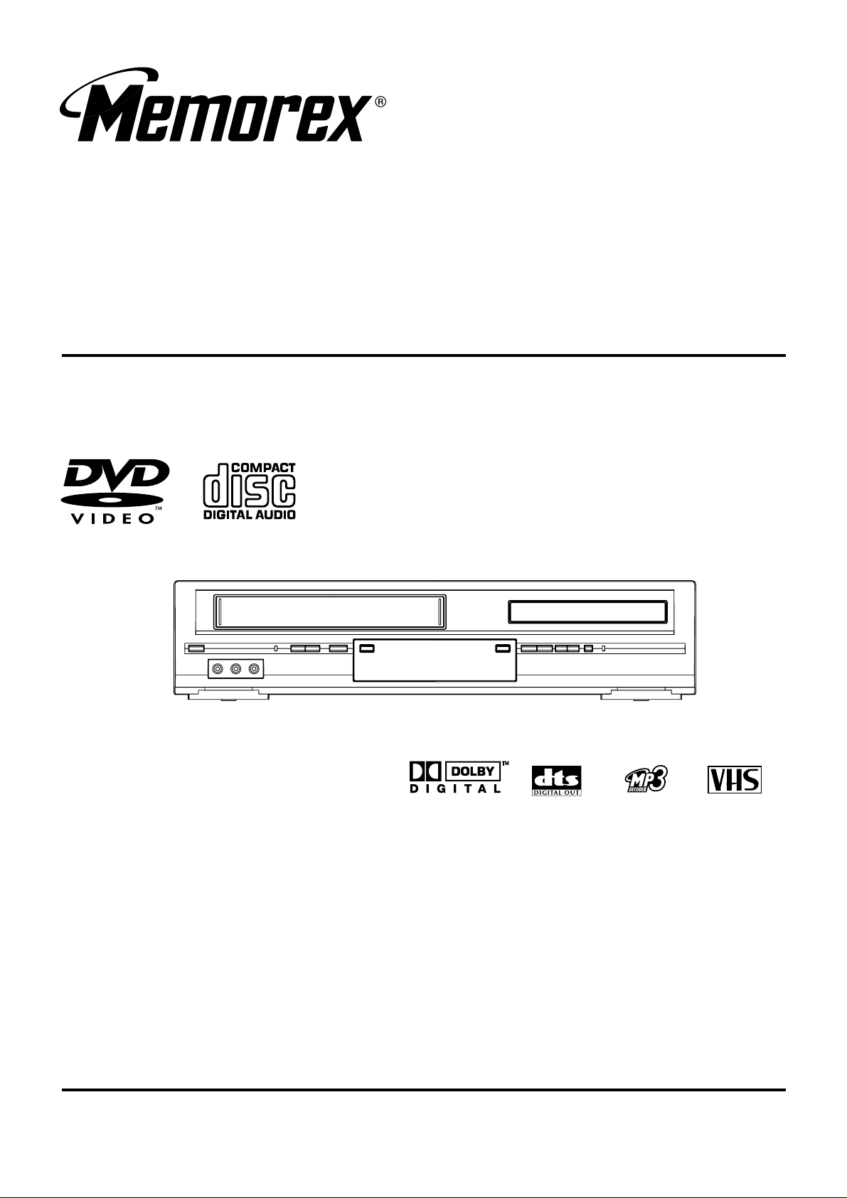
MVD4540C
SERVICE MANUAL
DVD VIDEO PLAYER & VHS VIDEO CASSETTE RECORDER
ORIGINAL
MFR'S VERSION A
Design and specifications are subject to change without notice.
Page 2
CAUTION
THIS DIGITAL VIDEO PLAYER EMPLOYS A LASER SYSTEM.
TO ENSURE PROPER USE OF THIS PRODUCT, PLEASE READ THIS SERVICE MANUAL CARE-
FULLY AND RETAIN FOR FUTURE REFERENCE. SHOULD THE UNIT REQUIRE MAINTENANCE,
CONTACT AN AUTHORIZED SERVICE LOCATION-SEE SERVICE PROCEDURE.
USE OF CONTROLS, ADJUSTMENTS OR THE PERFORMANCE OF PROCEDURES OTHER THAN
THOSE SPECIFIED HEREIN MAY RESULT IN HAZARDOUS RADIATION EXPOSURE.
TO PREVENT DIRECT EXPOSURE TO LASER BEAM, DO NOT TRY TO OPEN THE ENCLOSURE.
VISIBLE LASER RADIATION MAY BE PRESENT WHEN THE ENCLOSURE IS OPENED. DO NOT
STARE INTO BEAM.
Location of the required Marking
The rating sheet and the safety caution are on the rear of the unit.
CERTIFICATION: COMPLIES WITH FDA RADIATION PERFORMANCE
ST ANDARDS, 21 CFR SUBCHAPTER J.
PREPARATION OF SERVICING
The laser diode used for a pickup head may be destroyed with external static electricity.
Moreover, even if it is operating normally after repair, when static electricity discharge is received at the
time of repair, a life of product may become short.
Please perform the following measure against static electricity, be careful of destruction of a laser diode
enough at the time of repair, and work.
• It works on the desk which performed measures against static electricity, such as conductive mat.
• Soldering iron with ground wire or ceramic type is used.
• A worker needs to use a ground conductive wrist strap for body.
A1-1
Page 3
IMPORTANT SERVICE SAFETY INFORMATION
Safety precautions to be followed during servicing:
1.
Parts marked with an are critical parts for safety. Replace only with the one described in the parts
list.
2.
Before returning the DVD product to the customer, make the appropriate leakage current check or
resistance measurements to ensure that exposed parts are properly insulated from the supply circuit.
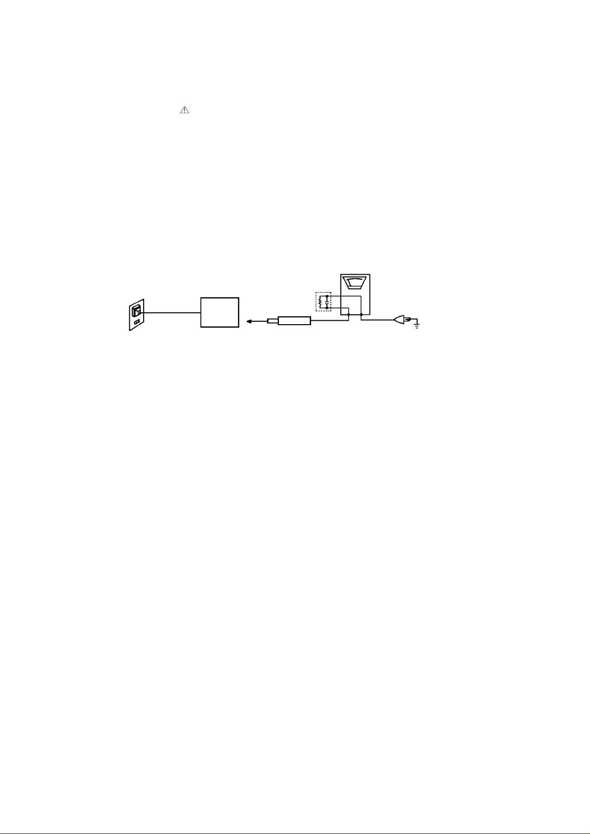
A leakage current check is recommended for this unit. Plug the AC line cord directly into a 120V 60Hz AC
outlet (do not use an isolation transformer for this check). Use a leakage current tester (Fig. 1) or a
metering system which complies with Underwriters Laboratories (UL 1409). Measure for current from all
exposed metal parts of the cabinet to a known earth ground: particularly, any exposed metal part having a
return path to the chassis. Any current measured must not exceed 0.5mA. Any measurement not within
the limits outlined above are indicative of a potential shock hazard and corrective action must be taken
before returning the unit to the customer.
(Reading should not be above 0.5mA)
Leakage Current Tester
PRODUCT UNDER TEST
1.5K ohm
0.15 µF
2-Blade polarized
type cord set
Test all exposed
metal surfaces
TEST PROBE
Fig. 1 AC Leakage Test
KNOWN EARTH
GROUND
A1-2
Page 4

IMPORTANT SAFEGUARDS
1.
READ INSTRUCTIONS
All the safety and operating instructions should be read before the unit is operated.
2.
RET AIN INSTRUCTIONS
The safety and operating instructions should be retained for future reference.
3.
HEED WARNINGS
All warnings on the unit and in the operating instructions should be adhered to.
4.
FOLLOW INSTRUCTIONS
All operating and use instructions should be followed.
5.
CLEANING
Unplug this unit from the wall outlet before cleaning. Do not use liquid cleaners or aerosol cleaners. Use a damp
cloth for cleaning.
6.
A TTACHMENTS
Do not use attachments not recommended by the unit’s manufacturer as they may cause hazards.
7.
WATER AND MOISTURE
Do not use this unit near water. For example, near a bathtub, washbowl, kitchen sink, or laundry tub, in a wet
basement, or near a swimming pool.
8.
ACCESSORIES
Do not place this unit on an unstable cart, stand, tripod, bracket, or table. The
unit may fall, causing serious injury, and serious damage to the unit. Use only
with a cart, stand, tripod, bracket, or table recommended by the manufacturer.
8A.
An appliance and cart combination should be moved with care. Quick stops,
excessive force, and uneven surfaces may cause the appliance and cart
combination to overturn.
9.
VENTILATION
Slots and openings in the cabinet and in the back or bottom are provided for ventilation, to ensure reliable
operation of the unit, and to protect it from overheating. These openings must not be blocked or covered. The
openings should never be blocked by placing the unit on a bed, sofa, rug, or other similar surface. This unit
should never be placed near or over a radiator or heat source. This unit should not be placed in a built-in
installation such as a bookcase or rack unless proper ventilation is provided or the manufacturer’s instructions
have been adhered to.
10.
POWER SOURCES
This unit should be operated only from the type of power source indicated on the rating plate. If you are not sure
of the type of power supply to your home, consult your appliance dealer or local power company . For units
intended to operate from battery power, or other sources, refer to the operating instructions.
11.
GROUNDING OR POLARIZA TION
This unit is equipped with a polarized alternating-current line plug (a plug having one blade wider than the other).
This plug will fit into the power outlet only one way . This is a safety feature. If you are unable to insert the plug
fully into the outlet, try reversing the plug. If the plug should still fail to fit, contact your electrician to replace your
obsolete outlet. Do not defeat the safety purpose of the polarized plug. If your unit is equipped with a 3-wire
grounding-type plug, a plug having a third (grounding) pin, this plug will only fit into a grounding-type power
outlet. This too, is a safety feature. If you are unable to insert the plug into the outlet, contact your electrician to
replace your obsolete outlet. Do not defeat the safety purpose of the grounding-type plug.
12.
POWER-CORD PROTECTION
Power-supply cords should be routed so that they are not likely to be walked on or pinched by items placed upon
or against them, paying particular attention to cords at plugs, convenience receptacles, and the point where they
exit from the appliance.
13.
LIGHTNING
To protect your unit from a lightning storm, or when it is left unattended and unused for long periods of time,
unplug it from the wall outlet and disconnect the antenna or cable system. This will prevent damage to the unit
due to lightning and power line surges.
14.
POWER LINES
An outside antenna system should not be located in the vicinity of overhead power lines or other electric light or
power circuits, or where it can fall into such power lines or circuits. When installing an outside antenna system,
extreme care should be taken to keep from touching such power lines or circuits, as contact with them might be
fatal.
15.
OVERLOADING
Do not overload wall outlets and extension cords, as this can result in a risk of fire or electric shock.
16.
OBJECT AND LIQUID ENTRY
Do not push objects through any openings in this unit, as they may touch dangerous voltage points or short out
parts that could result in fire or electric shock. Never spill or spray any type of liquid into the unit.
PORT ABLE CAR T WARNING
(symbol provided by RETAC)
S3125A
A1-3
Page 5

IMPORTANT SAFEGUARDS (CONTINUED)
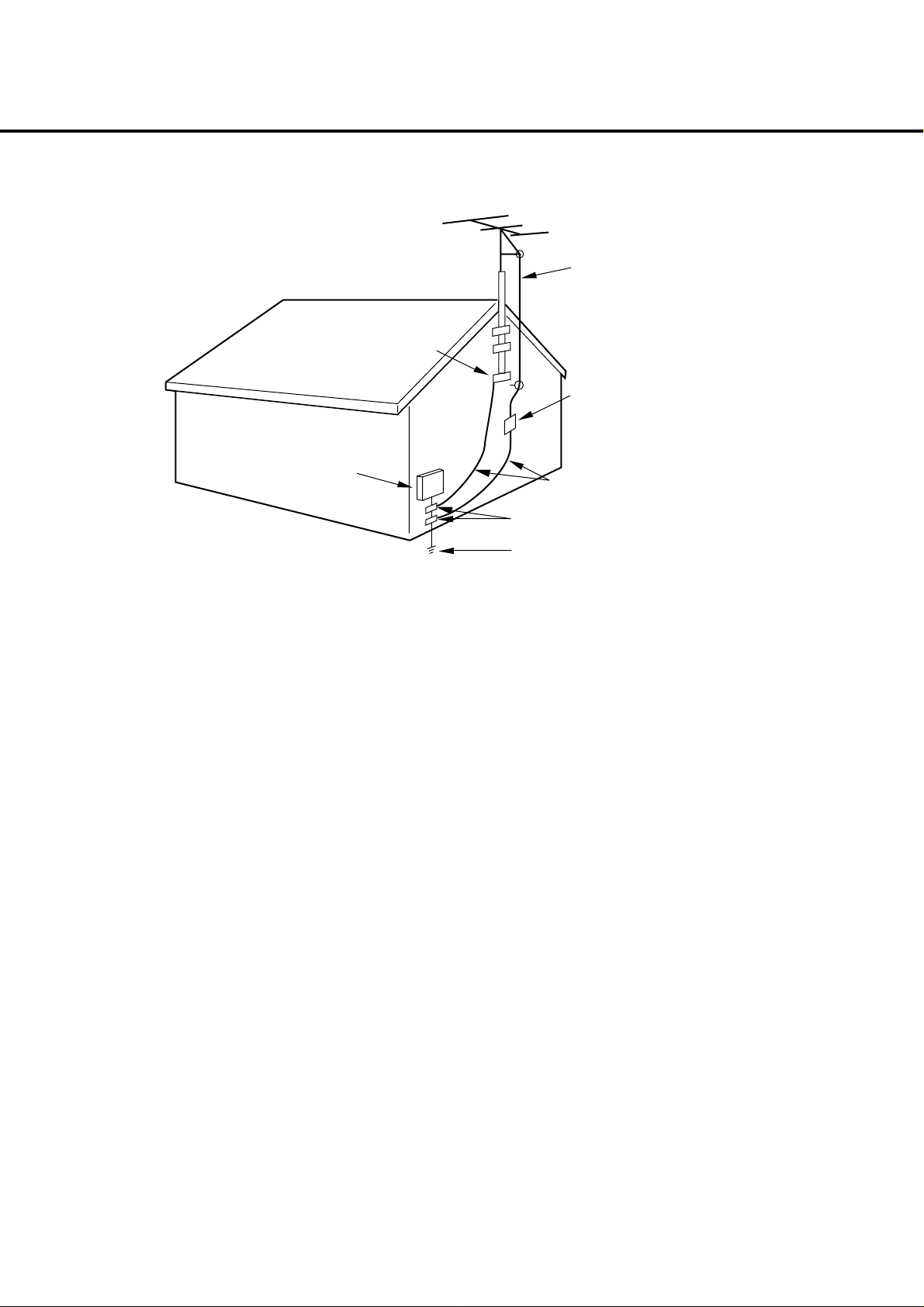
OUTDOOR ANTENNA GROUNDING
17.
If an outside antenna or cable system is connected to the unit, be sure the antenna or cable system is grounded
so as to provide some protection against voltage surges and built-up static charges. Section 810 of the National
Electrical Code, ANSI/NFPA 70, provides information with respect to proper grounding of the mast and supporting structure, grounding of the lead-in wire to an antenna discharge unit, size of grounding conductors, location of
antenna discharge unit, connection to grounding electrodes, and requirements for the grounding electrode.
SERVICING
18.
Do not attempt to service this unit yourself as opening or removing covers may expose you to dangerous voltage
or other hazards. Refer all servicing to qualified service personnel.
DAMAGE REQUIRING SERVICE
19.
Unplug this unit from the wall outlet and refer servicing to qualified service personnel under the following
conditions:
a.
When the power-supply cord or plug is damaged.
b.
If liquid has been spilled, or objects have fallen into the unit.
c.
If the unit has been exposed to rain or water.
d.
If the unit does not operate normally by following the operating instructions. Adjust only those controls that
are covered by the operating instructions, as an improper adjustment of other controls may result in
damage and will often require extensive work by a qualified technician to restore the unit to its normal
operation.
e.
If the unit has been dropped or the cabinet has been damaged.
f.
When the unit exhibits a distinct change in performance, this indicates a need for service.
REPLACEMENT P ARTS
20.
When replacement parts are required, be sure the service technician uses replacement parts specified by the
manufacturer or those that have the same characteristics as the original parts.
Unauthorized substitutions may result in fire, electric shock or other hazards.
SAFETY CHECK
21.
Upon completion of any service or repairs to this unit, ask the service technician to perform safety checks to
determine that the unit is in proper operating condition.
WALL OR CEILING MOUNTING
22.
The product should be mounted to a wall or ceiling only as recommended by the manufacturer.
HEAT
23.
The product should be situated away from heat sources such as radiators, heat registers, stoves, or other
products (including amplifiers) that produce heat.
DISC TRA Y
24.
Keep your fingers well clear of the disc tray as it is closing. It may cause serious personal injury.
CONNECTING
25.
When you connect the product to other equipment, turn off the power and unplug all of the equipment from the
wall outlet. Failure to do so may cause an electric shock and serious personal injury. Read the owner's manual of
the other equipment carefully and follow the instructions when making any connections.
SOUND VOLUME
26.
Reduce the volume to the minimum level before you turn on the product. Otherwise, sudden high volume sound
may cause hearing or speaker damage.
SOUND DISTORTION
27.
Do not allow the product output distorted sound for a longtime. It may cause speaker overheating and fire.
HEADPHONES
28.
When you use the headphones, keep the volume at a moderate level. If you use the headphones continuously
with high volume sound, it may cause hearing damage.
LEASER BEAM
29.
Do not look into the opening of the disc tray or ventilation opening of the product to see the source of the laser
beam. It may cause sight damage.
DISC
30.
Do not use a cracked, deformed, or repaired disc. These discs are easily broken and may cause serious personal
injury and product malfunction.
NOTE TO CATV SYSTEM INST ALLER
31.
This reminder is provided to call the CATV system installer’s attention to Article 820-40 of the NEC that provides
guidelines for proper grounding and, in particular, specifies that the cable ground shall be connected to the
grounding system of the building, as close to the point of cable entry as practical.
A1-4
Page 6
IMPORTANT SAFEGUARDS (CONTINUED)
EXAMPLE OF ANTENNA GROUNDING AS PER THE NATIONAL ELECTRICAL CODE
ANTENNA LEAD
IN WIRE
GROUND
CLAMP
ANTENNA
DISCHARGE UNIT
(NEC SECTION 810-20)
ELECTRIC SERVICE
EQUIPMENT
GROUNDING CONDUCTORS
(NEC SECTION 810-21)
GROUND CLAMPS
NEC-NATIONAL ELECTRICAL CODE
S2898A
POWER SERVICE GROUNDING
ELECTRODE SYSTEM
(NEC ART 250, PART H)
A1-5
Page 7
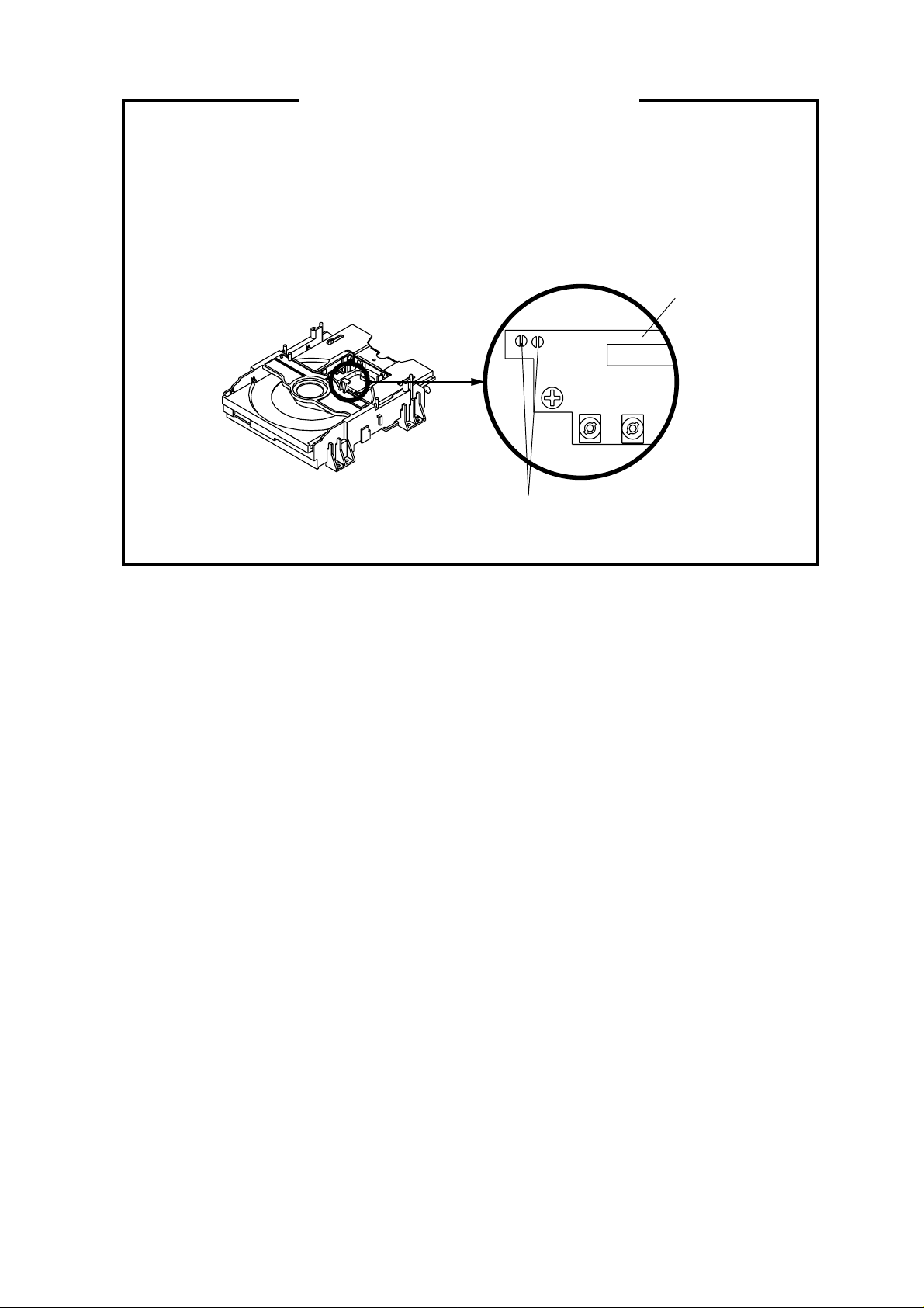
WHEN REPLACING DVD DECK
[ When the removal of the DVD Deck ]
Before removing Pick Up PCB and DVD PCB connector, make the short circuit on the position as
shown Fig. 1 using a soldering. If you remove the DVD Deck with no soldering, the Laser may be
damaged.
[ When the installation of the DVD Deck ]
Remove all the soldering on the short circuit position after the connection of Pick Up PCB and DVD
PCB connector.
Pick Up PCB
Make the sort circuit
using a soldering.
Fig. 1
A1-6
Page 8
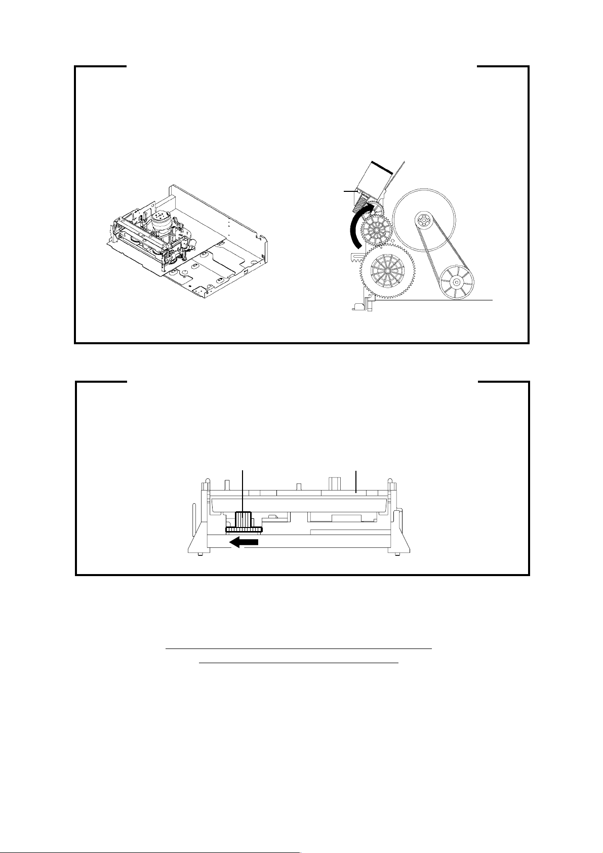
TAPE REMOVAL METHOD AT NO POWER SUPPLY
Remove the Top Cabinet, Front Cabinet and DVD Block. (Refer to item 1 of the
1.
DISASSEMBLY INSTRUCTIONS.)
Remove the screw 1 of the Deck Chassis and remove the Loading Motor. (Refer to Fig. 2)
2.
Rotate the Pinch Roller Cam in the direction of the arrow by hand to slacken the Video Tape.
3.
Rotate the Clutch Ass'y either of the derections to wind the Video Tape in the Cassette Case.
4.
Repeat the above step 3~4. Then take out the Video Cassette from the Deck Chassis. Be careful not to
5.
scratch on the tape.
Loading Motor
Screw 1
Capstan DD Unit
Pinch Roller Cam
Main Cam
Fig. 1
Main Chassis (Front Side)
Fig. 2
DISC REMOVAL METHOD AT NO POWER SUPPLY
1.
Remove the Back Cabinet and TV//DVD/VCR Block. (Refer to item 1 of the DISASSEMBLY
INSTRUCTIONS.)
2.
Rotate the Main Gear in the direction of the arrow by hand.
(Refer to Fig. 1)
3.
Draw the Tray.
DVD DeckMain Gear
Fig. 1
Clutch Ass'y
PARENTAL CONTROL - RATING LEVEL
4 DIGIT PASSWORD CANCELLATION
If the stored 4 digit password in the Rating Level menu needs to be cancelled, please follow the steps below.
Turn Unit ON.
1.
Press and hold the '7' key on the remote control unit.
2.
Simultaneously press and hold the 'STOP' key on the front panel.
3.
Hold both keys for more than 3 seconds.
4.
The On Screen Display message 'PASSWORD CLEAR' will appear.
5.
The 4 digit password has now been cleared
6.
A1-7
Page 9

CONTENTS
CAUTION ....................................................................................................................................
PREPARATION OF SERVICING ...............................................................................................
IMPORTANT SERVICE SAFETY INFORMATION ....................................................................
IMPORTANT SAFEGUARDS.....................................................................................................
WHEN REPLACING DVD DECK ...............................................................................................
TAPE REMOVAL METHOD AT NO POWER SUPPLY ............................................................
DISC REMOVAL METHOD AT NO POWER SUPPLY .............................................................
PARENTAL CONTROL-RATION LEVEL ..................................................................................
CONTENTS .................................................................................................................................
GENERAL SPECIFICATIONS ...................................................................................................
DISASSEMBLY INSTRUCTIONS
1. REMOVAL OF MECHANICAL PARTS AND P. C. BOARDS............................................
2. REMOVAL OF VCR DECK PARTS ...................................................................................
3. REMOVAL OF DVD DECK PARTS ...................................................................................
4. REMOVAL AND INSTALLATION OF FLAT PACKAGE IC ...............................................
KEY TO ABBREVIATIONS ........................................................................................................
SERVICE MODE LIST ................................................................................................................
PREVENTIVE CHECKS AND SERVICE INTERVALS..............................................................
WHEN REPLACING EEPROM (MEMORY) IC ..........................................................................
SERVICING FIXTURES AND TOOLS .......................................................................................
PREPARATION FOR SERVICING.............................................................................................
MECHANICAL ADJUSTMENTS ................................................................................................
ELECTRICAL ADJUSTMENTS..................................................................................................
BLOCK DIAGRAMS
DVD..........................................................................................................................................
Y/C/AUDIO/CCD/HEAD AMP .................................................................................................
SYSTEM CONTROL ..............................................................................................................
OPERATION/DISPLAY ..........................................................................................................
Hi-Fi/DEMODULATOR ...........................................................................................................
TUNER/JACK .........................................................................................................................
POWER ..................................................................................................................................
PRINTED CIRCUIT BOARDS
DVD..........................................................................................................................................
VCR/OPERATION ..................................................................................................................
LOADING MOTOR/SW ..........................................................................................................
SCHEMATIC DIAGRAMS
MPEG/MICON/DSP.................................................................................................................
MEMORY .................................................................................................................................
RF AMP/DSP ...........................................................................................................................
AUDIO/VIDEO .........................................................................................................................
Y/C/AUDIO/CCD/HEAD AMP ................................................................................................
SYSCON.................................................................................................................................
TUNER/JACK .........................................................................................................................
OPERATION/DISPLAY ..........................................................................................................
Hi-Fi/DEMODULATOR ...........................................................................................................
POWER ..................................................................................................................................
OPERATION/LED....................................................................................................................
LOADING MOTOR/SW ...........................................................................................................
INTERCONNECTION DIAGRAM ...............................................................................................
WAVEFORMS .............................................................................................................................
MECHANICAL EXPLODED VIEW .............................................................................................
CHASSIS EXPLODED VIEWS ...................................................................................................
DVD DECK EXPLODED VIEW...................................................................................................
MECHANICAL REPLACEMENT PARTS LIST .........................................................................
CHASSIS REPLACEMENT PARTS LIST..................................................................................
DVD DECK REPLACEMENT PARTS LIST...............................................................................
ELECTRICAL REPLACEMENT PARTS LIST...........................................................................
A1-1
A1-1
A1-2
A1-3~A1-5
A1-6
A1-7
A1-7
A1-7
A2-1
A3-1~A3-7
B1-1, B1-2
B2-1~B2-6
B3-1~B3-3
B4-1, B4-2
C1-1, C1-2
C2-1
C3-1, C3-2
C4-1
D1-1
D1-1
D2-1~D2-4
D3-1, D3-2
E-1, E-2
E-3, E-4
E-5, E-6
E-7, E-8
E-9, E-10
E-11, E-12
E-13, E-14
F-1, F-2
F-3~F-6
F-7, F-8
G-1, G-2
G-3, G-4
G-5, G-6
G-7, G-8
G-9, G-10
G-11, G-12
G-13, G-14
G-15, G-16
G-17, G-18
G-19, G-20
G-21, G-22
G-23, G-24
G-25, G-26
H-1~H-3
I1-1
I2-1, I2-2
I3-1
J1-1
J2-1
J3-1
J4-1, J4-2
A2-1
Page 10

GENERAL SPECIFICATIONS
G-1 Outline of the product DVD VIDEO PLAYER & VHS Player / Recorder
G-2 DVD System Color System NTSC
G-3 VCR System VHS Player / Recorder
System Video System NTSC
Disc DVD, CD-DA, CD-R/RW
Disc Diameter 120 mm , 80 mm
Deck Disc Loading System Front Disc Loading
Motor 3 Motors
Pick up 1-Lens 2-Beams System
Playback time (Max) DVD 1-Layer 135min (4.7GB)
DVD 2-Layer 245min (8.5GB)
CD 74min
VIDEO CD --min
Search speed Fwd 4 steps
Actual 2-45 times (DVD)
4-40 times (CD)
Rev 4 steps
Actual 2-45 times (DVD)
4-40 times (CD)
Slow speed Fwd 1/7-1/2 times
Actual --
Rev --
Actual --
Hi-Fi STEREO Yes
NTSC PB(PAL60Hz) No
Deck DECK OVD-7
Loading System Front
Motor 3
Heads Video Head 4Head
FM Audio Head 2Head
Audio / Control Mono/Yes
Erase (Full Track Erase) Yes
Tape Rec PAL Speed NTSC SP/SLP
Fast Forward / Rewind Time (Approx.) at 25oC FF:4'50"/REW:2'30"
Forward/Reverse NTSC or PAL-M SP/LP/SLP = 3x,5x / 7x,9x / 9x,15x
Picture Search PAL or SECAM Frame Advance Yes
Slow Speed 1/10
G-4 Tuning Broadcasting System US System M
System Tuner and System 1Tuner
Receive CH Destination US (w/CATV)
Intermediate Picture (FP) 45.75 MHz
Frequency Sound (FS) 41.25 MHz
Preset CH RF Converter Output Yes
Stereo / Dual TV Sound US-ST
Tuner Sound Muting Yes
Erase (Normal Audio Track Erase) No
Play PAL -
Channel 3 or 4 ch
Level / Impedance 66 dBu / 75 Ohm
Sound Selector No
NTSC SP/LP/SLP
with Cassette T-120
Tuning System F-Synth
Input Impedance VHF/UHF 75 OHM
CH Coverage
FP-FS 4.50 MHz
2-69,4A,A-5~ A-1,A~I,
J~ W, W+1-W+84
A3-1
Page 11
GENERAL SPECIFICATIONS
8 dBm/ 1k ohm (VCR
G-5 Power Power Source AC 120V 60Hz
Power Consumption 18 W at 120V 60Hz
Protector Power Fuse Yes
G-6 Regulation Safety UL
G-7 Temperature Operation 5oC - 40oC
G-8 Operating Humidity Less than 80% RH
G-9 Signal Video Signal Output Level 1 V p-p/75 ohm (DVD,VCR)
RGB Signal Output Level Audio Signal Input Level Microphone -
Hi-Fi Audio Signal Dynamic Range : More than 90dB
DC -
Stand by 2 W at 120V 60Hz
Per Year -- W
Safety Circuit Yes
IC Protector(Micro Fuse) No
Radiation FCC
Laser DHHS
Storage -20oC - 60oC
S/N Ratio (Weighted) 65 dB(DVD) 50 dB(VCR)
Horizontal Resolution 500 Lines (DVD) 230 Lines(VCR Mode)
Input Level Line -8 dBm/ 50k ohm (VCR, 0dBm=0.775Vrms)
Output Level Line
Digital Output Level 0.5 V p-p / 75 ohm(DVD)
S/N Ratio at (Weighted) 90dB(DVD), 42dB(VCR at SP)
Harmonic Distortion (1KHz) Typical
Frequency Response : DVD Mode at DVD 4 Hz - 22 KHz
DVD Mode at VIDEO CD -
DVD Mode at CD 4 Hz - 20 KHz
VCR Mode at SP 100Hz - 10 KHz
VCR Mode at LP -
VCR Mode at SLP 100Hz - 4 KHz
Frequency Response 20Hz ~20kHz
Wow And Flutter : Less than 0.01 %Wrms
Channel Separation : More than 60 dB
Harmonic Distortion : Less than 0.01
0dBm=0.775Vrms)
-12dBm/ 1k ohm (DVD, -20dBFs
0.02% (1KHz) (DVD) , 1.5% (1KHz) (VCR)
,
A3-2
Page 12

GENERAL SPECIFICATIONS
G-10 On Screen
Display (DVD) Menu Type Character
Menu
Language Yes
Menu Yes
Subtitle Yes
Audio Yes
Picture Yes
TV Screen Size Yes
OSD Display On/Off Yes
JPEG Interval No
Select Files No
E.B.L. (Enhanced Black Level) No
Sound Yes
DRC (Dynamic Range Control) Yes
Dialogue On:DRC(TV)/ Off:DRC(Std) No
dts Decode No
Output (5.1ch/2ch) No
Surround On/Off No
Center On/Off No
Sub Woofer On/Off No
Parental Yes
Password Lock/Unlock Yes
Rating Level Yes
Other Yes
OSD Language (Set up Language) Yes
Output (RGB / Composite) No
Open Yes
Close Yes
No disc Yes
Reading Yes
Play Yes
Still/Pause Yes
Stop Yes
Prohibit Mark Yes
Step Yes
Skip (>>|) Yes
Skip (|<<) Yes
Random Yes (CD, MP3)
Repeat Yes
Slow+ ## Yes
Slow- ## No
Search+ ## Yes
Search- ## Yes
Jump Yes
Resume Yes
Title No. Yes
Chapter No. Yes
Track No. Yes
Time Yes
Subtitle No. Yes
Angle No. Yes
Vocal On/Off Yes
Audio No. Yes
Audio Stereo L/R No
Zoom Yes
Marker No. Yes
Spatializer (N-2-2) No
Program Play Back Yes (CD, MP3)
MP3 Folder Name Yes
File Name Yes
File No Yes
Time Yes
Track No Yes
Progressive Scan Out ON/OFF Yes
Yes
A3-3
Page 13
GENERAL SPECIFICATIONS
P
(Symbo
)
C
ec,FF(Cue),Rew(Rev),Stop,
ject
On Screen Menu Yes
Display(VCR) Menu Type Character
G-CODE(or SHOWVIEW or PLUSCODE)No. Entry No
Stereo, Audio Output, SAP Yes
G-11 OSD Language DVD OSD English / French / Spanish
G-12 Clock,Timer Calendar 1990/1/1 ~ 2081/12/31
and Timer Timer Events 8 Program/ 1 Month
Back-up One Touch Recording Max Time 6 Hours
OTPB Valid Time No
Timer Back-up (at Power Off Mode) 5sec
G-13 Display DISPLAY Yes
Timer Rec Set Yes
Auto Repeat On/Off Yes
SAP On/Off Yes
CH Set-Up Yes
System Set Up Yes
lay/Stop/FF/Rew/Rec/OTR/Pause/Eject/Tape In/Repeat
VCR OSD English / French / Spanish
TV/CABLE Yes
Auto CH Memory Yes
Add/Delete Yes
Clock Set Yes (Calendar 12H)
Language Yes
No Noise Back Ground Yes
Auto Clock Yes
Standard Time Yes
Daylight Saving Time Yes
l Mark
CH/AV(LINE) Yes
Clock Yes
Repeat Yes
Tape Counter Yes
Index Yes
Tape Speed Yes
ATR / Manual Tracking Yes
ZERO Return Yes
Hi-Fi Yes
DISPLAY type LED Module (Green, "Rec" &Timer symbol = Red)
lock/Counter,CH,Timer Rec,OTR, Play
R
VCR Yes
DVD Yes
CD Yes
Clock
Counter VCR Yes (hour:min)
Eject Yes
Counter Remain No
Play Yes
Stop No
Rec Yes
FF / Cue No
REW / Review No
Pause / Still Yes
OTR (ITR) No
T-Rec Yes
Chapter No
TITLE No
TRACK Yes
Repeat No
Hi-Fi No
SP No
LP No
SLP No
CH Yes
RF Output CH Yes
Tape In Yes
Remocon Custom Code No
Progressive Scan Out Yes
ATR,E
DVD Yes (hour:min)
Yes
Yes (12h)
AM
Yes
PM
CD Yes (min:sec)
No
No
A3-4
Page 14

GENERAL SPECIFICATIONS
G-14 Remote Unit RC-JN
Control Glow in Dark Remocon No
G-15 Features Auto Power Off No
(DVD) Parental Lock Yes
Format NEC
Custom Code 71-8E
Power Source Voltage(D.C) 3V
Total Keys 46 Keys
Keys Power Yes
Video CD Playback No
MP3 Playback Yes
WMA Playback No
JPEG Playback No
Progressive Scan Out Yes
Digital Out Dolby Digital Yes
Down Mix Out (Dolby Digital) Yes
Spatializer (N-2-2)
Screen Saver
Tray Lock No
Auto Stop No
Audio DAC 192kHz / 24bit
UM size x pcs UM-4 x 2 pcs
DISPLAY Yes
1 Yes
2 Yes
3 Yes
4 Yes
5 Yes
6 Yes
7 Yes
8 Yes
9 Yes
0 Yes
Input Select No
Input Select / PROGRESSIVE Yes
UP/CH+ Yes
DOWN/CH- Yes
LEFT/ SET- / TRACKING- Yes
RIGHT/ SET+ / TRACKING+ Yes
VCR/DVD Yes
TV/VCR Yes
DVD MENU Yes
TOP MENU Yes
SETUP MENU/VCR MENU Yes
ENTER Yes
CANCEL Yes
RETURN Yes
PLAY Yes
STOP Yes
PAUSE/STILL/STEP Yes
FF(Cue)/SEARCH+ Yes
REW(Review)/SEARCH- Yes
REC/OTR Yes
SKIP+ / INDEX+ Yes
SKIP- / INDEX- Yes
AUDIO / AUDIO SELECT Yes
ANGLE/COUNTER RESET Yes
SUBTITLE/ATR Yes
PLAY MODE/SPEED Yes
T-REC Yes
CLOCK / COUNTER Yes
JUMP/ZERO RETURN Yes
ZOOM Yes
REPEAT A-B Yes
SLOW (Forward) Yes
MARKER Yes
OPEN/CLOSE Yes
EJECT Yes
MPEG Yes
PCM Yes
DTS Yes
(DTS) No
No
No
A3-5
Page 15

GENERAL SPECIFICATIONS
Features Auto Head Cleaning Yes
(VCR) Auto Tracking Yes
G-16 Accessories Owner's Manual Language English / Spanish
HQ (VHS Standard High Quality) Yes
Auto Power On, Auto Play, Auto Rewind, Auto Eject Yes
Auto Power Off No
Forward/Reverse Picture Search Yes
VIDEO PLUS+ (SHOWVIEW, G-CODE) No
One Touch Playback No
Auto CH Memory Yes
AREA CODE No
Auto Clock Set Yes
Index Search Yes
SQPB No
CATV Yes
Energy Star No
MTS (SAP) Yes
CM Skip (30sec x 6 Times) No
Copy (Disc to Tape) No
w/Guarantee Card Yes
Remote Control Unit Yes
Guarantee Card No
Registration Card No
Warning Sheet No
Service Station List No
Important Tag No
AC Plug Adapter No
Quick Set-up Sheet No
Battery No
UM size x pcs -AC Cord No
AV Cord (1.2m) Yes
75 Ohm Coaxial Cable (0.9m) Yes
S-Video Cable No
21pin cable No
800 No Sticker No
Toll Free Insert Sheet No
Safety Tip No
A3-6
Page 16
GENERAL SPECIFICATIONS
G-17 Interface Switch Front Power Yes
Rear Attenuator No
Volume Phones Volume No
Terminals Front Video In RCA x1 (Yellow)
Rear Video Output RCA x1 (Yellow)
Indicator LED Power No
G-18 Set Size Approx. W x D x H (mm) 430 x 227 x 99
G-19 Weight Net (Approx.) 3.5 kg( 7.7lbs)
G-20 Carton Master Carton No
Gift Box Yes
Drop Test
Container Stuffing 2,011 Sets/40' container
G-21 Material Cabinet Front PS 94V2 or More / DECABROM
PCB Non-Halogen Demand No
G-22 Environment Pb Free Lead-free Solder No
Cd Free No
Play Yes
Eject (VCR) Yes
Stop Yes
Rec/OTR Yes
Open/Close (DVD) Yes
CH + Yes
CH - Yes
FF/ Search(>>) Yes
Rew/Search(<<) Yes
Still/Pause No
Shuttle (Search/REV/FWD) No
DVD/VCR Yes
Main Power SW No
S-Video/Component Video Selector Yes
RF Out (Slide SW) No
Main Power SW No
Mic Volume No
Echo Volume No
Rec/OTR No
Audio In RCA x 2 (Stereo, White/Red)
S-Video x 1 (DVD Signal Only)
Component x1 (RCA 3pin,DVD Signal Only)
Audio Output RCA x 4 (Stereo, White/Red)
Coaxial x 1 (Digital Audio,DVD Signal Only)
Optical Out (Option) Yes (Digital Audio,DVD Signal Only)
Video Input (Option) No
Audio Input (Option) No
RF Input / Output Yes
Euro Scart No
AC Inlet No
Rec No
T-Rec No
TV/VCR No
DVD Yes (RED)
VCR Yes (RED)
Surround No
Level Meter No
Gross (Approx.) 4.5 kg( 9.9lbs)
Content --- Sets
Material --- / --Dimensions W x D x H(mm) --Description of Origin ---
Material Double / Brown
W/Color Photo Label No
Dimensions W x D x H(mm) 497 x 340 x 180
Design As Per BUYER 's
Description of Origin Yes
Natural Dropping At 1 Corner / 3 Edges / 6 Surfaces
Height (cm) 80 cm
Eyelet Demand No
Other No
A3-7
Page 17
DISASSEMBLY INSTRUCTIONS
1.
REMOVAL OF MECHANICAL PARTS
AND P.C. BOARDS
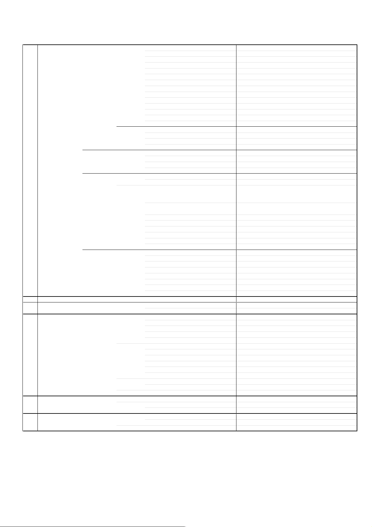
1-1:
TOP CABINET/FRONT CABINET/OPERATION PCB
(Refer to Fig. 1-1)
1.
Remove the 5 screws 1.
2.
Remove the Top Cabinet in the direction of arrow (A).
3.
Disconnect the following connector: (CP651).
4.
Unlock the 8 supports 2.
5.
Remove the Front Cabinet in the direction of arrow (B).
6.
Remove the 2 screws 3.
7.
Remove the Operation PCB in the direction of arrow (C).
Top Cabinet
1
(A)
Front Cabinet
(B)
2
2
2
2
2
2
3
3
2
(C)
Operation PCB
2
1-2: FLAP (Refer to Fig. 1-2)
1.2.Open Flap to 90˚ and flex in direction of arrow (A), at
the same time slide in direction of arrow (B).
Then lift in direction of arrow (C).
1
1
1
1
Fig. 1-1
1-3: DVD DECK/DVD PCB (Refer to Fig. 1-3)
1.
Make the short circuit on the position as shown Fig. 1-3
using a soldering. If you remove the DVD Deck with no
soldering, the Laser may be damaged.
2.
Unlock the support 1 and remove the Deck Top Holder
in the direction of arrow (A).
3.
Remove the 2 screws 2.
4.
Remove the 2 screws 3.
5.
Disconnect the following connectors:
(CP501, CP8001).
6.
Remove the DVD Deck in the direction of arrow (B).
7.
Remove the 2 screws 4.
8.
Remove the DVD PCB in the direction of arrow (C).
9.
Remove the 3 screws 5.
10.
Remove the Front Angle in the direction of arrow (D).
4
4
(C)
3
2
DVD PCB
Make the sort circuit
using a soldering.
Pick Up PCB
Fig. 1-3
Deck Top Holder
5
5
DVD Deck
3
2
1
(A)
(B)
5
(D)
Front Angle
(C)
(B)
(A)
NOTE
When the installation of the DVD Deck, remove all the
soldering on the short circuit position after the connection
of Pick Up PCB and VCR PCB connector.
Flap
Fig. 1-2
B1-1
Page 18
DISASSEMBLY INSTRUCTIONS
1-4: VCR DECK (Refer to Fig. 1-4)
NOTE
Do not remove the cable at the FE Head section. The FE
Head may be damaged if you remove the cable by force.
1.
Remove the screw 1.
2.
Remove the FE Head.
3.
Move the Cassette Holder Ass’y to the back side.
4.
Remove the 2 screws 2.
5.
Remove the 2 screws 3.
6.
Disconnect the following connectors:
(CP101, CP102, CP3001).
7.
Remove the VCR Deck in the direction of arrow.
2
1
FE Head
2
VCR Deck
3
3
1-5: VCR PCB (Refer to Fig. 1-5)
1.
Remove the screw 1.
2.
Remove the 5 screws 2.
3.
Remove the 2 screws 3.
4.
Remove the 3pin Shield.
5.
Remove the VCR PCB in the direction of arrow.
3
3
VCR PCB
3pin Shield
1
Fig. 1-4
2
2
2
2
2
Fig. 1-5
B1-2
Page 19
DISASSEMBLY INSTRUCTIONS
2. REMOVAL OF VCR DECK PARTS
2-1: TOP BRACKET (Refer to Fig. 2-1)
Extend the 2 supports 1.
1.
Slide the 2 supports 2 and remove the Top Bracket.
2.
NOTE
1. After the installation of the Top Bracket, bend the
support 1 so that the Top Bracket is fixed.
Top Bracket
1
Top Bracket
2
Main Chassis
2
Main Chassis
2-2: CASSETTE HOLDER ASS'Y (Refer to Fig. 2-2)
Move the Cassette Holder Ass'y to the front side.
1.
Push the Locker R to remove the Cassette Side R.
2.
Remove the Cassette Side L.
3.
Main Chassis
Cassette Side R
1
Fig. 2-1
Locker R
NOTE
1.2.In case of the Locker R installation, check if the one
position of Fig.2-3-B are correctly locked.
When you install the Cassette Side R, be sure to move
the Locker R after installing.
Locker R
Check if this position
Cassette Side R
is locked.
Fig. 2-3-B
2-4: LINK UNIT (Refer to Fig. 2-4)
Set the Link Unit to the Eject position.
1.
Unlock the support 1.
2.
Remove the (A) side of the Link Unit first, then remove
3.
the (B) side.
Main Chassis
Link Unit
Link Unit
Cassette Side L
Main Chassis
Fig. 2-2
2-3: CASSETTE SIDE L/R (Refer to Fig. 2-3-A)
Remove the Locker Spring.
1.
Unlock the 4 supports 1 and then remove the Cassette
2.
Side L/R.
Unlock the support 2 and then remove the Locker R.
3.
Locker Spring
1
1
2
Cassette Holder
Locker R
1
1
(A)
1
(B)
Link Unit
Main Chassis
2-5: LINK LEVER/FLAP LEVER (Refer to Fig. 2-5)
Extend the support 1.
1.
Remove the Link Lever.
2.
Remove the Flap Lever.
3.
1
Flap Lever
Link Lever
Fig. 2-4
Fig. 2-5
Cassette Side R
Cassette Side L
Fig. 2-3-A
B2-1
Page 20
DISASSEMBLY INSTRUCTIONS
2-6: LOADING MOTOR/WORM (Refer to Fig. 2-6-A)
Remove the screw 1.
1.
Remove the Loading Motor.
2.
Remove the Worm.
3.
Loading Motor
Worm
Main Chassis
• Screw Torque: 3 ± 0.5kgf•cm
1
Fig. 2-6-A
NOTE
1.
In case of the Worm installation, check if the value of
the Fig. 2-6-B is correct.
2.
In case of the Loading Motor installation, hook the wire
on the Cassette Opener as shown Fig. 2-6-C.
3.
When installing the wires between Capstan DD Unit
and Loading Motor, connect them correctly as shown
Fig. 2-6-D.
2-7: TENSION ASS'Y (Refer to Fig. 2-7-B)
Turn the Pinch Roller Cam clockwise so that the
1.
Tension Holder hook is set to the position of Fig. 2-7-A
to move the Tension Arm Ass'y.
Remove the Tension Spring.
2.
Unlock the 2 supports 1 and remove the Tension
3.
Band.
Unlock the support 2 and remove the Tension Arm
4.
Ass'y.
Unlock the support 3 and remove the Tension
5.
Connect.
Float the hook 4 and turn it clockwise then remove the
6.
Tension Holder.
Tension Arm Ass'y
Fig. 2-7-A
1
Tension Connect
Tension Spring
2
4
1
3
Tension Holder
Tension Band
Tension Arm Ass'y
19.2 ± 0.1mm
Safety surface for pressing
of the insert.
Loading Motor
Cassette Opener
Fig. 2-6-B
Fig. 2-6-C
Loading Motor Capstan DD Unit
-
Pink
L2
Fig. 2-7-B
NOTE
1.
In case of the Tension Band installation, note the
direction of the installation. (Refer to Fig. 2-7-C)
2.
In case of the Tension Band installation, install correctly
as Fig. 2-7-D.
3.
In case of the Tension Connect installation, install as
the circled section of Fig. 2-7-E.
Tension Connect
Tension Band
Fig. 2-7-C
[OK]
[NG]
Tension Connect
Tension Connect
Tension Band
Tension Band
Fig. 2-7-D
+
White
L1
Fig. 2-6-D
Tension Connect
Main Chassis
Fig. 2-7-E
B2-2
Page 21
DISASSEMBLY INSTRUCTIONS
2-8: T BRAKE ARM/T BRAKE BAND (Refer to Fig. 2-8-A)
Remove the T Brake Spring.
1.
Turn the T Brake Arm clockwise and bend the hook
2.
section to remove it.
Unlock the 2 supports 1 and remove the T Brake
3.
Band.
Idler Gear
S Reel
Idler Arm Ass'y
(B)
T Brake Band
Hook section
1
1
T Brake Arm
T Brake Spring
Fig. 2-8-A
NOTE
1. In case of the T Brake Band installation, install correctly
as Fig. 2-8-B.
[OK]
T Brake Band
[NG]
T Brake Band
T Brake Arm
T Brake Arm
(A) T Reel
1
(A)
1
Fig. 2-9-A
NOTE
1.2.In case of the S Reel and T Reel installation, check if the
correct parts are installed. (Refer to Fig. 2-9-B)
In case of the Idler Arm Ass'y installation, install correctly
as Fig. 2-9-C. And also set it so that the section "B" of
Fig. 2-9-A is placed under the Main Chassis tab.
Fig. 2-8-B
2-9: S REEL/T REEL/IDLER ARM ASS'Y/IDLER GEAR
(Refer to Fig. 2-9-A)
Remove the S Reel and T Reel.
1.
Remove the 2 Polyslider Washers 1.
2.
Remove the Idler Arm Ass'y and Idler Gear.
3.
NOTE
Take care not to damage the gears of the S Reel and T
1.
Reel.
The Polyslider Washer may be remained on the back of
2.
the reel.
Take care not to damage the shaft.
3.
Do not touch the section "A" of S Reel and T Reel. (Use
4.
gloves.) (Refer to Fig. 2-9-A) Do not adhere the stains
on it.
When you install the reel, clean the shaft and grease it
5.
(FG-84M). (If you do not grease, noise may be heard in
FF/REW mode.)
After installing the reel, adjust the height of the reel.
6.
(Refer to MECHANICAL ADJUSTMENT)
[OK]
[NG]
Clutch Gear
Clutch Gear
Big Hole
(S Reel)
Small Hole
(T Reel)
Fig. 2-9-B
Idler Arm Ass'y
Idler Arm Ass'y
Fig. 2-9-C
B2-3
Page 22
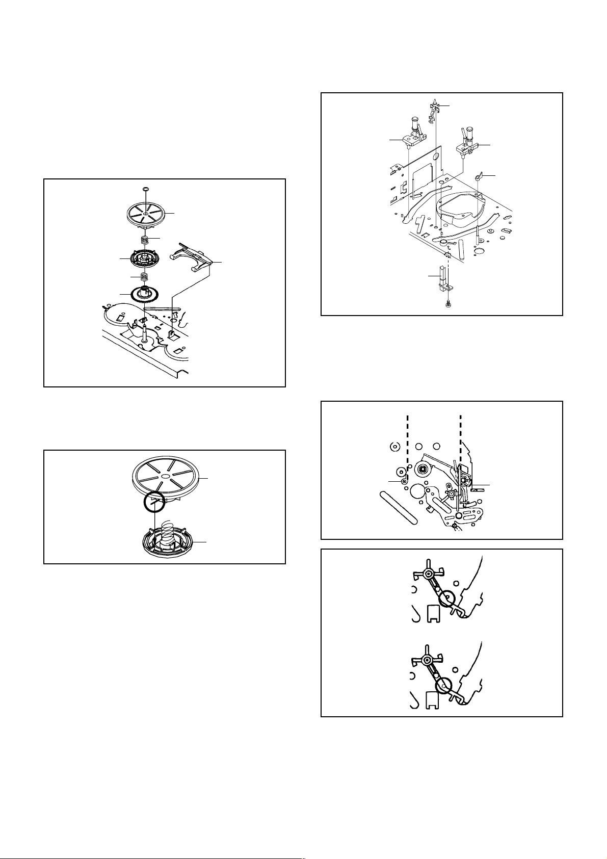
DISASSEMBLY INSTRUCTIONS
2-10: CASSETTE OPENER/PINCH ROLLER BLOCK/
P5 ARM ASS'Y (Refer to Fig. 2-10-A)
Unlock the support 1 and remove the Cassette
1.
Opener.
Remove the Pinch Roller Block and P5 Arm Ass'y.
2.
1
Cassette Opener
Pinch Roller Block
P5 Arm Ass'y
Main Chassis
Fig. 2-10-A
NOTE
Do not touch the Pinch Roller. (Use gloves.)
1.
In case of the Pinch Roller Block and the Pinch Roller
2.
Cam installation, install correctly as Fig. 2-10-B.
Pinch Roller Block
P5 Arm Ass'y
Can be seen the hole of the
Main Cam.
Can be seen the hole of
the Pinch Roller Cam.
Fig. 2-10-B
2-11: A/C HEAD (Refer to Fig. 2-11-A)
Remove the screw 1.
1.
Remove the A/C Head Base.
2.
Remove the 3 screws 2.
3.
Remove the A/C Head and A/C Head Spring.
4.
NOTE
1.
Do not touch the A/C Head. (Use gloves.)
2.
When you install the A/C Head Spring, install as shown in
Fig. 2-11-B.
3.
When you install the A/C Head, tighten the screw (1) first,
then tighten the screw (2), finally tighten the screw (3).
(3)
(1)
2
2
(2)
1
2
A/C Head
A/C Head Spring
Spring Position
Fig. 2-11-B
2-12: FE HEAD (RECORDER ONLY) (Refer to Fig. 2-12)
Remove the screw 1.
1.
Remove the FE Head.
2.
1
FE Head
• Screw Torque: 5 ± 0.5kgf•cm
• The FE Head is not installed on the Video Cassette Player.
Fig. 2-12
2-13: AHC ASS'Y/CYLINDER UNIT ASS'Y
(Refer to Fig. 2-13)
Unlock the support 1 and remove the AHC Ass'y.
1.
Disconnect the following connector:
2.
(CD2001)
Remove the 3 screws 2.
3.
Remove the Cylinder Unit Ass'y.
4.
NOTE
When you install the Cylinder Unit Ass'y, tighten the
1.
screws from (1) to (3) in order while pulling the Ass'y
toward the left front direction.
Cylinder Unit Ass'y
AHC Ass'y
1
(3)
(2)
(1)
• Screw Torque: 3 ± 0.5kgf•cm
2
2
2
Fig. 2-13
• Screw Torque: 5 ± 0.5kgf•cm (Screw 1)
A/C Head Base
Fig. 2-11-A
B2-4
Page 23
DISASSEMBLY INSTRUCTIONS
2-14: CAPSTAN DD UNIT (Refer to Fig. 2-14)
Remove the Capstan Belt.
1.
Remove the screw 1.
2.
Remove the Capstan Holder.
3.
Remove the 3 screws 2.
4.
Remove the Capstan DD Unit.
5.
Pinch Roller Cam
Marker
Main Cam
1
2
2
2
• Screw Torque: 4 ± 0.5kgf•cm
2-15:
MAIN CAM/PINCH ROLLER CAM/JOINT GEAR
Capstan Belt
Capstan Holder
Capstan DD Unit
(Refer to Fig. 2-15-A)
Remove the E-Ring 1, then remove the Main Cam.
1.
Remove the E-Ring 2, then remove the Pinch Roller
2.
Cam and Joint Gear.
1
Fig. 2-14
Fig. 2-15-B
2-16: LOADING GEAR S/T UNIT (Refer to Fig. 2-16-A)
1.2.Remove the E-Ring 1 and remove the Main Loading
Gear.
Remove the Main Rod, Tension Lever, Loading Arm S
Unit and Loading Arm T Unit.
1
Main Rod
Tension Lever
Main Loading Gear
Loading Arm T Unit
Loading Arm S Unit
Fig. 2-16-A
Main Cam
2
Pinch Roller Cam
Joint Gear
Fig. 2-15-A
NOTE
1.
In case of the Pinch Roller Cam and Main Cam
installation, install them as the circled section of Fig. 215-B so that the each markers are met. (Refer to Fig.
2-15-B)
NOTE
When you install the Loading Arm S Unit, Loading Arm
1.
T Unit and Main Loading Gear, align each marker.
(Refer to Fig. 2-16-B)
Marker
Main Loading Gear
Marker
Loading Arm T Unit
Loading Arm S Unit
Fig. 2-16-B
B2-5
Page 24
DISASSEMBLY INSTRUCTIONS
2-17:
CLUTCH ASS'Y/RING SPRING/CLUTCH LEVER/
CLUTCH GEAR (Refer to Fig. 2-17-A)
Remove the Polyslider Washer 1.
1.
Remove the Clutch Ass'y and Ring Spring.
2.
Remove the Clutch Lever.
3.
Remove the Coupling Gear, Coupling Spring and
4.
Clutch Gear.
1
Clutch Ass'y
Ring Spring
Inclined Base S
Unit
1
Cassette Guide Post
Inclined Base T
Unit
P4 Cap
Coupling Gear
Coupling Spring
Clutch Gear
Clutch Lever
Fig. 2-17-A
NOTE
In case of the Clutch Ass'y installation, install it with
1.
inserting the spring of the Clutch Ass'y into the dent of
the Coupling Gear. (Refer to Fig. 2-17-B)
Clutch Ass'y
Coupling Gear
Fig. 2-17-B
2-18:
CASSETTE GUIDE POST/INCLINED BASE S/T
UNIT/P4 CAP/LED REFLECTOR
(Refer to Fig. 2-18-A)
Remove the P4 Cap.
1.
Unlock the support 1 and remove the Cassette Guide
2.
Post.
Remove the Inclined Base S/T Unit.
3.
Remove the screw 2.
4.
Remove the LED Reflector.
5.
LED Reflector
• Screw Torque: 5 ± 0.5kgf•cm
2
Fig. 2-18-A
NOTE
Do not touch the roller of Guide Roller.
1.
In case of the P4 Cap installation, install it with parallel
2.
for "A" and "B" of Fig. 2-18-B.
In case of the Cassette Guide Post installation, install
3.
correctly as the circled section of Fig. 2-18-C.
"A"
P4 Cap
"B"
Cassette Opener
Fig. 2-18-B
[OK]
Cassette Guide Post
[NG]
Cassette Guide Post
B2-6
Fig. 2-18-C
Page 25

DISASSEMBLY INSTRUCTIONS
3. REMOVAL OF DVD DECK PARTS
NOTE
1. Do not disassemble the DVD DECK PARTS except
listed parts here. Minute adjustments are needed if the
disassemble is done. If the repair is needed except
listed parts, replace the DVD MECHA ASS'Y.
3-1: TRAY (Refer to Fig. 3-1-A)
Set the Tray opened. (Refer to the DISC REMOVAL
1.
METHOD AT NO POWER SUPPLY)
Unlock the 2 supports 1 and remove the Tray.
2.
Main Frame Ass'y
Tray
NOTE
In case of the Tray installation, install them as the
1.
circled section of Fig. 3-1-B so that the each markers
are met.
1
1
Fig. 3-1-A
NOTE
In case of the Main Chassis Ass'y, install it from (1) to
1.
(4) in order. (Refer to Fig. 3-2-B)
In case of the Main Chassis Ass'y installation, hook the
2.
wire on the Main Frame Ass'y as shown Fig. 3-2-C.
Main Frame Ass'y (Bottom Side)
(3)
Rack Loading
(3)
(2)
(4)
Check Lock
Main Frame Ass'y
(3)
Traverse Holder
(1)
Main Chassis Ass'y
(4)
Fig. 3-2-B
Main Frame Ass'y
Tray
Fig. 3-1-B
3-2: MAIN CHASSIS ASS'Y (Refer to Fig. 3-2-A)
Remove the screw 1.
1.
Unlock the 2 supports 2.
2.
Remove the Insulator (R) from the Main Frame Ass'y.
3.
Remove the Main Chassis Ass'y.
4.
1
2
2
Main Frame Ass'y
Insulator (R)
Check Hook
Fig. 3-2-C
3-3: LOADING MOTOR PCB ASS'Y/ LOADING BELT
(Refer to Fig. 3-3-A)
1.
Remove the Loading Belt.
2.
Remove the screw 1.
3.
Remove the 2 screws 2.
4.
Remove the Loading Motor PCB Ass'y.
5.
Remove the Pulley Gear.
Loading Belt
2
2
Main Frame Ass’y
Pulley Gear
1
• Screw Torque: 2.5 ± 0.3kgf•cm (Screw 1)
• Screw Torque: 1.0 ± 0.3kgf•cm (Screw 2)
Loading Motor PCB Ass’y
Fig. 3-3-A
Main Chassis Ass'y
• Screw Torque: 2.0 ± 0.5kgf•cm
Fig. 3-2-A
B3-1
Page 26

DISASSEMBLY INSTRUCTIONS
NOTE
1.
In case of the Pulley Motor installation, check if the
value of the Fig. 3-3-B is correct.
2.
When installing the Loading Motor PCB Ass'y, install it
correctly as Fig. 3-3-C.
3.
In case of the Loading Motor PCB Ass'y installation,
hook the wire on the Main Frame Ass'y as shown Fig.
3-3-C.
Pulley Motor
Loading Motor
Rack Loading
Safety surface for pressing
of the insert.
The Lever should be position
between A and B.
7.0 ± 0.1mm
Fig. 3-3-B
AB
3-5: CLAMPER ASS'Y (Refer to Fig. 3-5-A)
Press the Clamper and rotate the Clamper Plate
1.
clockwise, then unlock the 3 supports 1.
Remove the Clamper Plate, Clamper Magnet and
2.
Clamper.
Clamper Plate
Clamper Magnet
Main Frame
1
1
Clamper
1
Fig. 3-5-A
NOTE
1. In case of the Clamper Ass'y installation, install
correctly as Fig. 3-5-B.
Clamper Plate
Check Hook
Loading Motor PCB Ass’y
Fig. 3-3-C
3-4: RACK LOADING/MAIN GEAR/PULLEY GEAR
(Refer to Fig. 3-4-A)
1.
Press down the catcher 1 and slide the Rack Loading.
2.
Unlock the support 2 and remove the Pulley Gear.
3.
Remove the Main Gear.
Pulley Gear
Main Gear
2
1
Rack Loading
Main Frame Ass’y
Fig. 3-4-A
NOTE
1. In case of the Rack Loading installation, do not mesh it
to the Main Gear as shown the Fig. 3-4-B.
Rack Loading
Check Hook
Clamper
No gap
Fig. 3-5-B
3-6:
TRAVERSE HOLDER/INSULATOR (F)/INSULATOR
(R) (Refer to Fig. 3-6-A)
Remove the Traverse Holder.
1.
Remove the 2 Insulator (F).
2.
Remove the Insulator (R).
3.
Main Chassis Ass'y
Insulator (F)
Traverse Holder
Insulator (F)
Insulator (R)
Fig. 3-6-A
NOTE
1.2.In case of the Insulator (F) installation, install correctly
as Fig. 3-6-B.
In case of the Insulator (R) installation, install correctly
as Fig. 3-6-C.
Main Gear
Fig. 3-4-B
Insulator (F)
Traverse Holder
Fig. 3-6-B
B3-2
Page 27

DISASSEMBLY INSTRUCTIONS
Insulator (R)
3-7:
RACK FEED ASS'Y/SWITCH PCB ASS'Y/FEED
Main Chassis Ass'y (Top Side)
MOTOR (Refer to Fig. 3-7-A)
Remove the screw 1.
1.
Remove the Rack Feed Ass'y.
2.
Remove the screw 2.
3.
Remove the Switch PCB Ass'y.
4.
Remove the 2 screw 3.
5.
Remove the Feed Motor.
6.
Remove the Motor Gear.
7.
1
2
Switch PCB Ass'y
Main Chassis Ass'y
• Screw Torque: 5.0 ± 0.3kgf•cm (Screw 1)
• Screw Torque: 3.0 ± 0.3kgf•cm (Screw 2)
• Screw Torque: 1.0 ± 0.3kgf•cm (Screw 3)
• Screw Torque: 3.5 ± 0.3kgf•cm (Screw 4)
Rack Feed Ass'y
3
3
Fig. 3-6-C
Motor Gear
Feed Motor
Fig. 3-7-A
~ FEED MOTOR ~
Switch PCB Ass'y
~ SPINDLE MOTOR ~
• Install wire from (1) to (4) in order.
Main Chassis Ass'y (Bottom Side)
Check Hook
Check Hook
• Loosen the wire in the direction of the arrow.
Check Hook
BLUE (4)
ORANGE (3)
BLACK (2)
RED (1)
Fig. 3-7-D
Check Hook
Fig. 3-7-E
NOTE
1.
When pushing the Rack Feed in the direction of the
arrow, it should be restored to the original position by
the spring force. (Refer to Fig. 3-7-B)
2.
In case of the Motor Gear installation, check if the value
of the Fig. 3-7-C is correct.
3.
When installing the wire of the Switch PCB Ass'y, install
it correctly as Fig. 3-7-D.
4.
After the assembly of the Main Chassis Ass'y, hook the
wire on the Main Chassis Ass'y as shown Fig. 3-7-E.
Push
Rack Feed Ass'y
Fig. 3-7-B
Motor Gear
Feed Motor
6.0 ± 0.2mm
Safety surface for pressing
of the insert.
Fig. 3-7-C
B3-3
Page 28

DISASSEMBLY INSTRUCTIONS
4.
REMOVAL AND INSTALLATION OF
FLAT PACKAGE IC
REMOVAL
Put the Masking Tape (cotton tape) around the Flat
1.
Package IC to protect other parts from any damage.
(Refer to Fig. 4-1.)
NOTE
Masking is carried out on all the parts located within
10 mm distance from IC leads.
When IC starts moving back and forth easily after
3.
desoldering completely, pickup the corner of the IC using
a tweezers and remove the IC by moving with the IC
desoldering machine. (Refer to Fig. 4-3.)
NOTE
Some ICs on the PCB are affixed with glue, so be
careful not to break or damage the foil of each IC
leads or solder lands under the IC when removing it.
Blower type IC
desoldering
machine
Masking Tape
(Cotton Tape)
Heat the IC leads using a blower type IC desoldering
2.
IC
machine. (Refer to Fig. 4-2.)
NOTE
Do not add the rotating and the back and forth
directions force on the IC, until IC can move back and
forth easily after desoldering the IC leads completely.
Blower type IC
desoldering machine
Fig. 4-1
Tweezers
IC
Peel off the Masking Tape.4.
Absorb the solder left on the pattern using the Braided
5.
Shield Wire. (Refer to Fig. 4-4.)
NOTE
Do not move the Braided Shield Wire in the vertical
direction towards the IC pattern.
Fig. 4-3
Braided Shield Wire
Soldering Iron
IC
Fig. 4-2
IC pattern
Fig. 4-4
B4-1
Page 29

DISASSEMBLY INSTRUCTIONS
INSTALLATION
Take care of the polarity of new IC and then install the
1.
new IC fitting on the printed circuit pattern. Then solder
each lead on the diagonal positions of IC temporarily.
(Refer to Fig. 4-5.)
Soldering Iron
Solder temporarily
Supply the solder from the upper position of IC leads
2.
Solder temporarily
sliding to the lower position of the IC leads.
(Refer to Fig. 4-6.)
Fig. 4-5
When bridge-soldering between terminals and/or the
4.
soldering amount are not enough, resolder using a Thintip Soldering Iron. (Refer to Fig. 4-8.)
Thin-tip Soldering Iron
IC
Fig. 4-8
Finally, confirm the soldering status on four sides of the
5.
IC using a magnifying glass.
Confirm that no abnormality is found on the soldering
position and installation position of the parts around the
IC. If some abnormality is found, correct by resoldering.
NOTE
When the IC leads are bent during soldering and/or
repairing, do not repair the bending of leads. If the
bending of leads are repaired, the pattern may be
damaged. So, always be sure to replace the IC in this
case.
Soldering IronSolder
IC
Absorb the solder left on the lead using the Braided
3.
Supply soldering
from upper position
to lower position
Shield Wire. (Refer to Fig. 4-7.)
NOTE
Do not absorb the solder to excess.
Soldering Iron
IC
Braided Shield Wire
Fig. 4-6
Fig. 4-7
B4-2
Page 30

A
A/C
ACC
AE
AFC
AFT
AFT DET
AGC
AMP
ANT
A.PB
APC
ASS’Y
AT
AUTO
A/V
B
BGP
BOT
BPF
BRAKE SOL
BUFF
B/W
C
C
CASE
CAP
CARR
CH
CLK
CLOCK (SY-SE)
COMB
CONV
CPM
CTL
CYL
CYL-M
CYL SENS
D
DATA (SY-CE)
dB
DC
DD Unit
DEMOD
DET
DEV
E
E
EF
EMPH
ENC
ENV
EOT
EQ
EXT
F
F
FBC
FE
FF
FG
FL SW
FM
FSC
FWD
G
GEN
GND
H
H.P.F
KEY TO ABBREVIATIONS
:
Audio/Control
:
Automatic Color Control
:
Audio Erase
:
Automatic Frequency Control
:
Automatic Fine Tuning
:
Automatic Fine Tuning Detect
:
Automatic Gain Control
:
Amplifier
:
Antenna
:
Audio Playback
:
Automatic Phase Control
:
Assembly
:
All Time
:
Automatic
:
Audio/Video
:
Burst Gate Pulse
:
Beginning of Tape
:
Bandpass Filter
:
Brake Solenoid
:
Buffer
:
Black and White
:
Capacitance, Collector
:
Cassette
:
Capstan
:
Carrier
:
Channel
:
Clock
:
Clock (Syscon to Servo)
:
Combination, Comb Filter
:
Converter
:
Capstan Motor
:
Control
:
Cylinder
:
Cylinder-Motor
:
Cylinder-Sensor
:
Data (Syscon to Servo)
:
Decibel
:
Direct Current
:
Direct Drive Motor Unit
:
Demodulator
:
Detector
:
Deviation
:
Emitter
:
Emitter Follower
:
Emphasis
:
Encoder
:
Envelope
:
End of Tape
:
Equalizer
:
External
:
Fuse
:
Feed Back Clamp
:
Full Erase
:
Fast Forward, Flipflop
:
Frequency Generator
:
Front Loading Switch
:
Frequency Modulation
:
Frequency Sub Carrier
:
Forward
:
Generator
:
Ground
:
High Pass Filter
H.SW
Hz
I
IC
IF
IND
INV
K
KIL
L
L
LED
LIMIT AMP
LM, LDM
LP
L.P.F
LUMI.
M
M
MAX
MINI
MIX
MM
MOD
MPX
MS SW
N
NC
NR
O
OSC
OPE
P
PB
PB CTL
PB-C
PB-Y
PCB
P. CON
PD
PG
P-P
R
R
REC
REC-C
REC-Y
REEL BRK
REEL S
REF
REG
REW
REV, RVS
RF
RMC
RY
S
S. CLK
S. COM
S. DATA
SEG
SEL
SENS
SER
SI
SIF
SO
SOL
SP
STB
SW
:
Head Switch
:
Hertz
:
Integrated Circuit
:
Intermediate Frequency
:
Indicator
:
Inverter
:
Killer
:
Left
:
Light Emitting Diode
:
Limiter Amplifier
:
Loading Motor
:
Long Play
:
Low Pass Filter
:
Luminance
:
Motor
:
Maximum
:
Minimum
:
Mixer, mixing
:
Monostable Multivibrator
:
Modulator, Modulation
:
Multiplexer, Multiplex
:
Mecha State Switch
:
Non Connection
:
Noise Reduction
:
Oscillator
:
Operation
:
Playback
:
Playback Control
:
Playback-Chrominance
:
Playback-Luminance
:
Printed Circuit Board
:
Power Control
:
Phase Detector
:
Pulse Generator
:
Peak-to Peak
:
Right
:
Recording
:
Recording-Chrominance
:
Recording-Luminance
:
Reel Brake
:
Reel Sensor
:
Reference
:
Regulated, Regulator
:
Rewind
:
Reverse
:
Radio Frequency
:
Remote Control
:
Relay
:
Serial Clock
:
Sensor Common
:
Serial Data
:
Segment
:
Select, Selector
:
Sensor
:
Search Mode
:
Serial Input
:
Sound Intermediate Frequency
:
Serial Output
:
Solenoid
:
Standard Play
:
Serial Strobe
:
Switch
C1-1
Page 31

S
SYNC
SYNC SEP
T
TR
TRAC
TRICK PB
TP
U
UNREG
V
V
VCO
VIF
VP
V.PB
VR
V.REC
VSF
VSR
VSS
V-SYNC
VT
X
X’TAL
Y
Y/C
KEY TO ABBREVIATIONS
:
Synchronization
:
Sync Separator, Separation
:
Transistor
:
Tracking
:
Trick Playback
:
Test Point
:
Unregulated
:
Volt
:
Voltage Controlled Oscillator
:
Video Intermediate Frequency
:
Vertical Pulse, Voltage Display
:
Video Playback
:
Variable Resistor
:
Video Recording
:
Visual Search Fast Forward
:
Visual Search Rewind
:
Voltage Super Source
:
Vertical-Synchronization
:
Voltage Tuning
:
Crystal
:
Luminance/Chrominance
C1-2
Page 32

SERVICE MODE LIST
This unit provided with the following SERVICE MODES so you can repair, examine and adjust easily.
To enter to the SERVICE MODE function, press and hold both buttons simultaneously on the main unit or on the main unit
and on the remote control for more than a standard time in the appropriate condition. (See below chart.)
In case of the main unit and remote control, press the remote control buttons first, then press the main unit buttons.
Set
Condition
VCR mode
VCR mode
VCR mode
(Playback)
Power Off
Set
Condition
DVD mode
(No disc)
DVD mode
(No disc)
Set Key Operations
CH UP
CH UP PLAY 2 sec.
CH UP STOP 2 sec.
CH DOWN POWER 2 sec.
Set Key
REC/OTR 4 2 sec.
STOP 7 3 sec.
Set Key
FF 2 sec.
Remocon
Key
Standard
Time
Standard
Time
PLAY/REC total hours are displayed on the TV Monitor.
Refer to the “PREVENTIVE CHECKS AND SERVICE INTERVALS”
(CONFIRMATION OF HOURS USED).
Can be checked of the INITIAL DATA of MEMORY IC.
Refer to the “WHEN REPLACING EEPROM (MEMORY) IC”.
Initialization of the factory on VCR.
NOTE: Do not use this for the normal servicing.
If you set a factory initialization, the memories are reset
such as the clock setting, the channel setting, and PLAY/
REC total hours.
Adjust the PG SHIFTER automatically.
Refer to the “ELECTRICAL ADJUSTMENT”.
VCR operation mode at no connection of DVD.
Refer to the “PREPARATION FOR SERVICING”
NOTE:
Initialization of the factory on DVD.
NOTE:
Releasing of PARENTAL LOCK.
Refer to the “PARENTAL CONTROL - RATING LEVEL”.
NOTE:
Although the DVD is connected, the DVD mode cannot be
selected.
Operations
Do not use this for the normal servicing.
This function will only work without the setting of DVD
disc at DVD mode. While pressing the Remocon Key for
more than 2 seconds, press the Set Key simultaneously.
The function will only work without the setting of DVD disc
at DVD mode.
Method Operations
Press the ATR button on the
remote control for more than
2 seconds during PLAY.
Make the short circuit
between the test point of
SERVICE and the GND.
Adjusting of the Tracking to the center position.
Refer to the “MECHANICAL ADJUSTMENT” (GUIDE ROLLER) and “ELECTRICAL
ADJUSTMENT” (PG SHIFTER).
The BOT, EOT, and the Reel Sensor do not work and the VCR deck can be operated
without a cassette tape.
Refer to the “PREPARATION FOR SERVICING”
C2-1
Page 33

PREVENTIVE CHECKS AND SER VICE INTERVALS
The following standard table depends on environmental conditions and usage.
Parts replacing time does not mean the life span for individual parts.
Also, long term storage or misuse may cause transformation and aging of rubber parts.
The following list means standard hours, so the checking hours depends on the conditions.
Time
Parts Name
Audio Control Head
Full Erase Head
(Recorder only)
Capstan Belt
Pinch Roller
Capstan DD Unit
Loading Motor
Tension Band
T Brake Band
Clutch Ass’y
Idler Arm Ass’y
Capstan Shaft
Tape Running
Guide Post
Cylinder Unit
: Clean
: Check it and if necessary, replace it.
500
hours
1,000
hours
1,500
hours
2,000
hours
2,500
hours
Notes
Clean those parts in
contact with the tape.
Clean the rubber, and parts
which the rubber touches.
Replace when rolling
becomes abnormal.
Clean the Head
CONFIRMATION OF HOURS USED
PLAY/REC total hours can be checked on the screen.
Total hours are displayed in 16 system of notation.
NOTE: If you set a factory initialization, the total hours is reset to “0”.
1.
Connect the set to TV Monitor.
2.
Turn on the POWER, and set to the VCR mode.
3.
Press both CH UP button on the set and the FF button on the set for more than 2 seconds.
The Fig. 1 screen will appear on TV Monitor.
4.
After the confirmation of using hours, turn off the power.
INIT 00 0E
PLAY/REC 0010
Fig. 1
Initial setting content of MEMORY IC.
PLAY/REC total hours.
= (16 x 16 x 16 x thousands digit value)
+ (16 x 16 x hundreds digit value)
+ (16 x tens digit value)
+ (ones digit value)
C3-1
Page 34

PREVENTIVE CHECKS AND SER VICE INTERVALS
CLEANING
NOTE
After cleaning the heads with isopropyl alcohol, do not
run a tape until the heads dry completely. If the heads
are not completely dry and alcohol gets on the tape,
damage may occur.
1. AUDIO CONTROL HEAD
Clean the Audio Control Head with the cotton stick
soaked by alcohol. Clean the full erase head in the
same manner. (Refer to the figure below.)
Audio Control Head
2. TAPE RUNNING SYSTEM
When cleaning the tape transport system, use the
gauze moistened with isopropyl alcohol.
3. CYLINDER
Wrap a piece of chamois around your finger. Dip it in
isopropyl alcohol. Hold it to the cylinder head softly.
Turn the cylinder head counterclockwise to clean it (in
the direction of the arrow). (Refer to the figure below.)
NOTE
Do not exert force against the cylinder head. Do not move
the chamois upward or downward on the head.
Use the chamois one by one.
Cylinder Head
C3-2
Page 35

WHEN REPLACING EEPROM (MEMORY) IC
If a service repair is undertaken where it has been required to change the MEMORY IC, the following steps should be taken to
ensure correct data settings while making reference to TABLE 1.
NOTE: INI 34 and INI 35 cannot be set. Because, the total time for the PLAY/REC of the main unit is recorded.
INIT
+0 +1 +2 +3 +4 +5 +6 +7 +8 +9 +A +B +C +D +E +F
00
0E 10 DC 60 64 64 4A 86 0B 2B 86 32 0A 08 0A 01
10
AF 97 95 8A A0 57 31 04 88 A5 9F 3A 00 10 BF 00
20
3A 11 22 70 61 2A 3A 00 0B 00 40 C5 9A B0 00 37
30
03 17 --- --- --- --- --- --- --- --- --- --- --- --- --- ---
Table 1
1.
Connect the set to TV Monitor.
2.
Turn on the POWER, and set to the VCR mode.
3.
Press both CH UP button on the set and the FF button on the set for more than 2 seconds.
ADDRESS and DATA will appear on TV Monitor as Fig 1.
ADDRESS DATA
INIT 00 0E
PLAY/REC 0010
Fig. 1
4.
ADDRESS is now selected and should “blink”. Using the Tracking + or - button on the remote, step through the ADDRESS
until required ADDRESS to be changed is reached.
5.
Press ENTER to select DATA. When DATA is selected, it will “blink”.
6.
Again, step through the DATA using Tracking + or - button until required DATA value has been selected.
7.
Pressing ENTER will take you back to ADDRESS for further selection if necessary.
8.
Repeat steps 4 to 7 until all data has been checked.
9.
When satisfied correct DATA has been entered, turn POWER off (return to STANDBY MODE) to finish DATA input.
After the data input, set to the initializing of shipping.
10.
Turn on the POWER, and set to the VCR mode.
11.
Press both CH UP button on the set and the PLAY button on the set for more than 2 seconds.
12.
After the finishing of the initializing of shipping, the unit will turn off automatically.
The unit will now have the correct DATA for the new MEMORY IC.
C4-1
Page 36

SERVICING FIXTURES AND TOOLS
(For 2 heads model)
VHS Alignment Tape
JG001
JG001A
JG001Q
JG001T
(VN2S-LI63)
(VN2S-CO13)
(VN2S-LI63H)
2S-X6
(VN
Screwdriver
JG154 Cable
(For 4 heads model)
VHS Alignment Tape
JG001B
JG001I
3
)
JG001P
JG001S
(VN
(VN1S-CO13)
(VN1S-LI63H)
(VN
1S-LI6
1S-X6
3
)
3
)
JG002B
JG002E
JG002F
JG024AJG022 Master PlaneJG153 X Value Adjustment
Adapter
Dial Torque Gauge
(10~90gf•cm)
(60~600gf•cm)
Reel Disk Height
Adjustment Jig
JG005 Post Adjustment
Screwdriver
Part No. SV-TG0-030-000
(small)
JG100A Torque Tape
(VHT-063)
JG185 Tentelometer
Ref. No.
JG001
JG001A APJG001A00
JG001Q
JG001T
JG001B
JG001I
JG001P
JG001S
JG002B
JG002E
JG002F
JG005
JG153
JG022
JG024A
JG100A
JG154 APJG154000 Cable Used to connect the test point of SERVICE and GROUND
JG185 APJG185000 Tentelometer Confirmation of Tape Tension on Playback
Part No.
APJG001000
APJG001Q00
APJG001T00
APJG001B00
APJG001I00
APJG001P00
APJG001S00 VHS Alignment Tape X Value Adjustment (For 4 heads model)
APJG002B00
APJG002E00
APJG002F00
APJG005000
APJG153000
APJG022000
APJG024A00
APJG100A00
VHS Alignment Tape
VHS Alignment Tape
VHS Alignment Tape
VHS Alignment Tape
VHS Alignment Tape
VHS Alignment Tape
VHS Alignment Tape
Adapter
Dial Torque Gauge (10~90gf•cm)
Dial Torque Gauge (60~600gf•cm)
Post Adjustment Screwdriver
X Value Adjustment Screwdriver
Master Plane
Reel Disk Height Adjustment Jig
Torque Tape (VHT-063)
Parts Name
Remarks
Monoscope, 6KHz (For 2 heads model)
Color Bar, 1KHz (For 2 heads model)
Hi-Fi Audio (For 2 heads model)
X Value Adjustment (For 2 heads model)
Monoscope, 6KHz (For 4 heads model)
Color Bar, 1KHz (For 4 heads model)
Hi-Fi Audio (For 4 heads model)
VSR Torque, Brake Torque (S Reel/T Reel Ass'y)
Brake Torque (T Reel Ass'y)
VSR Torque, Brake Torque (S Reel)
Guide Roller Adjustment
X Value Adjustment
Reel Disk Height Adjustment
Reel Disk Height Adjustment
Playback Torque, Back Tension Torque During Playback
PREPARATION FOR SERVICING
1.
While pressing the CH DOWN button on the set for more than 2 seconds, press the POWER button on the set
simultaneously at the Power OFF. Although the DVD is connected, the DVD mode cannot be selected.
2.
Short circuit between TP3001 and Ground with the cable JG154.
(The BOT, EOT, and the Reel Sensor do not work and the VCR deck can be operated without a cassette tape.)
3.
In case of using a cassette tape, press the STOP/EJECT button to insert or eject a cassette tape.
Turn on the power and re-check the cable before checking the trouble points.
When you servicing with connection of DVD, perform the operations above step 2 to step 3.
D1-1
Page 37

MECHANICAL ADJUSTMENTS
1. CONFIRMATION AND ADJUSTMENT
Read the following NOTES before starting work.
• Place an object which weighs between 450g~500g on
the Cassette Tape to keep it steady when you want to
make the tape run without the Cassette Holder. (Do not
place an object which weighs over 500g.)
1-1: CONFIRMATION AND ADJUSTMENT OF REEL
DISK HEIGHT
1.
Turn on the power and set to the STOP mode.
2.
Set the master plane (JG022) and reel disk height
adjustment jig (JG024A) on the mechanism framework,
taking care not to scratch the drum, as shown in Fig. 1-
1-A.
3.
While turning the reel and confirm the following points.
Check if the surface “A” of reel disk is lower than the
surface “B” of reel disk height adjustment jig (JG024A)
and is higher than the surface “C”. If it is not passed,
place the height adjustment washers and adjust to
10(+2, -0)mm.
4.
Adjust the other reel in the same way.
Master Plane (JG022)
Reel Disk Height Adjustment Jig
(JG024A)
1-2: CONFIRMATION AND ADJUSTMENT OF TENSION
POST POSITION
1.
Set to the PLAY mode.
2.
Adjust the adjusting section for the Tension Arm
position so that the Tension Arm top is within the
standard line of Main Chassis.
3.
While turning the S Reel clockwise, confirm that the
edge of the Tension Arm is located in the position
described above.
Standard line of Main Chassis
Tension Arm
0.5mm (Adjusting range)
Fig. 1-2-A
Adjusting section for the
Tension Arm position
Tension Band
Master Plane (JG022)
10(+0.2, -0)mm
Reel Disk
(B)
Height Adjustment Washer
2.6x4.7xT0.13
2.6X4.7xT0.25
Fig. 1-1-A
Reel Disk Height
Adjustment Jig
(JG024A)
(C)
(A)
Fig. 1-1-B
The Tension Arm top will
move to the inside direction
of the Main Chassis.
Bend
The Tension Arm top will
move to the outside direction
of the Main Chassis.
Fig. 1-2-B
1-3: CONFIRMATION OF PLAYBACK TORQUE AND
BACK TENSION TORQUE DURING PLAYBACK
1.2.Load a video tape (T-120) recorded in standard speed
mode. Set the unit to the PLAY mode.
Install the tentelometer (JG185) as shown in Fig. 1-3.
Confirm that the meter indicates 20 ± 2gf in the beginning of playback.
• USING A CASSETTE TYPE TORQUE TAPE (JG100A)
1.
After confirmation and adjustment of Tension Post
position (Refer to item 1-2), load the cassette type
torque tape (JG100A) and set to the PLAY mode.
2.
Confirm that the right meter of the torque tape indicates
50~90gf•cm during playback in SP mode.
3.
Confirm that the left meter of the torque tape indicates
25~40gf•cm during playback in SP mode.
Tentelometer
(JG185)
Video Tape
D2-1
P1 Post Guide Roller
Fig. 1-3
Page 38

MECHANICAL ADJUSTMENTS
1-4: CONFIRMATION OF VSR TORQUE
1.2.Install the Torque Gauge (JG002F) and Adapter (JG002B)
on the S Reel. Set to the Picture Search (Rewind) mode.
(Refer to Fig.1-4-B)
Then, confirm that it indicates 120~180gf•cm.
NOTE
Install the Torque Gauge on the reel disk firmly. Press the
REW button to turn the reel disk.
1-5: CONFIRMATION OF REEL BRAKE TORQUE
(S Reel Brake) (Refer to Fig. 1-4-B)
1.
Once set to the Fast Forward mode then set to the Stop
mode. While, unplug the AC cord when the Pinch Roller
Block is on the position of Fig. 1-4-A.
2.
Move the Idler Ass’y from the S Reel.
3.
Install the Torque Gauge (JG002F) and Adapter
(JG002B) on the S Reel. Turn the Torque Gauge
(JG002F) clockwise.
4.
Then, confirm that it indicates 60~100gf•cm.
(T Reel Brake) (Refer to Fig. 1-4-B)
1.
Once set to the Fast Forward mode then set to the Stop
mode. While, unplug the AC cord when the Pinch Roller
Block is on the position of Fig. 1-4-A.
2.
Move the Idler Ass’y from the T Reel.
3.
Install the Torque Gauge (JG002E) and Adapter
(JG002B) on the T reel. Turn the Torque Gauge
(JG002E) counterclockwise.
4.
Then, confirm that it indicates 30~50gf•cm.
Stop at this position.
The position at
STOP mode.
Capstan DD Unit
The position at FF mode.
Cassette Holder Ass’y
Pinch Roller Block
Cassette Opener
Fig. 1-4-A
NOTE
If the torque is out of the range, replace the following parts.
Check item
1-4
1-5
S Reel side:
Replacement Part
Idler Ass’y/Clutch Ass’y
S Reel/Tension Band/Tension
Connect/T ension Arm Ass’y
T Reel side:
T Reel/T Brake Band//T Brake
Spring/T Brake Arm
2. CONFIRMA TION AND ADJUSTMENT
OF TAPE RUNNING MECHANISM
Tape Running Mechanism is adjusted precisely at the
factory. Adjustment is not necessary as usual. When you
replace the parts of the tape running mechanism because
of long term usage or failure, the confirmation and adjustment are necessary.
2-1: GUIDE ROLLER
1.
Playback the VHS Alignment Tape (JG001 or JG001B).
(Refer to SERVICING FIXTURE AND TOOLS)
2.
Connect CH-1 of the oscilloscope to TP101 (Envelope)
and CH-2 to TP3002 (SW Pulse).
3.
Press and hold the ATR button on the remote control
more than 2 seconds to set tracking to center.
4.
Trigger with SW Pulse and observe the envelope. (Refer
to Fig. 2-1-A)
5.
When observing the envelope, adjust the Adjusting
Driver (JG005) slightly until the envelope will be flat.
Even if you press the Tracking Button, adjust so that
flatness is not moved so much.
6.
Adjust so that the A : B ratio is better than 3 : 2 as shown
in Fig. 2-1-B, even if you press the Tracking Button to
move the envelope (The envelope waveform will begin to
decrease when you press the Tracking Button).
7.
Adjust the PG shifter during playback.
(Refer to the ELECTRICAL ADJUSTMENTS)
NOTE
After adjustment, confirm and adjust A/C head.
(Refer to item 2-2)
Torque Gauge/Adapter
(JG002F/JG002B)
S Reel
Torque Gauge/Adapter
(JG002E/JG002B)
T Reel
Fig. 1-4-B
D2-2
CH-1
Envelope
(TP101)
CH-2
SW Pulse (TP3002)
Entrance
Max
CH-1
Track
A : B ≥ 3 : 2
CH-2
Track
Fig. 2-1-A
Exit
MaxA B
Fig. 2-1-B
Page 39

MECHANICAL ADJUSTMENTS
2-2: CONFIRMA TION AND ADJUSTMENT OF AUDIO/
CONTROL HEAD
When the Tape Running Mechanism does not work well,
adjust the following items.
1.
Playback the VHS Alignment Tape (JG001 or JG001B).
(Refer to SERVICING FIXTURE AND TOOLS)
2.
Confirm that the reflected picture of stamp mark is
appeared on the tape prior to P4 Post as shown in Fig.
2-2-A.
a)
When the reflected picture is distorted, turn the screw
1 clockwise until the distortion is disappeared.
b)
When the reflected picture is not distorted, turn the
screw 1 counterclockwise until little distortion is
appeared, then adjust the a).
3.
Turn the screw 2 to set the audio level to maximum.
4.
Confirm that the bottom of the Audio/ Control Head and
the bottom of the tape is shown in Fig. 2-2-C.
c)
When the height is not correct, turn the screw 3 to
adjust the height. Then, adjust the 1~3 again.
Audio/Control Head
Reflected picture of
Stamp Mark
P4 Cap
2-3: TAPE RUNNING ADJUSTMENT
(X VALUE ADJUSTMENT)
1.
Confirm and adjust the height of the Reel Disk.
(Refer to item 1-1)
2.
Confirm and adjust the position of the Tension Post.
(Refer to item 1-2)
3.
Adjust the Guide Roller. (Refer to item 2-1)
4.
Confirm and adjust the Audio/Control Head.
(Refer to item 2-2)
5.
Connect CH-1 of the oscilloscope to TP3002, CH-2 to
TP101 and CH-3 to HOT side of Audio Out Jack.
6.
Playback the VHS Alignment Tape (JG001S or JG001T).
(Refer to SERVICING FIXTURE AND TOOLS)
7.
Press and hold the ATR button on the remote control
more than 2 seconds to set tracking to center.
8.
Set the X Value adjustment driver (JG153) to the 4 of
Fig. 2-2-B. Adjust X value so that the envelope waveform
output becomes maximum. Check if the relation between
Audio and Envelope waveform becomes (1) or (2) of Fig.
2-3.
Envelope
(1)
CH-3
Audio
(2)
3
2
Audio/Control Head
Tape
Stamp Mark
Audio/Control Head
1
4
Fig. 2-2-A
Fig. 2-2-B
0.25±0.05mm
Fig. 2-2-C
Fig. 2-3
2-4: CONFIRM HI-FI AUDIO (Hi-Fi model only)
1.
Connect CH-1 of the oscilloscope to TP101 and CH-2 to
the Hi-Fi Audio Out Jack.
2.
Playback the VHS Alignment Tape (JG001P or JG001Q).
(Refer to SERVICING FIXTURE AND TOOLS)
3.
Press and hold the ATR button on the remote control
more than 2 seconds to set tracking to center.
4.
Press the Tracking Up button and count number of steps
which the audio output is changed from Hi-Fi (10KHz) to
MONO (6KHz).
5.
Press and hold the ATR button on the remote control
more than 2 seconds to set tracking to center.
6.
Press the Tracking Down button and count number of
steps which the audio output is changed from Hi-Fi
(10KHz) to MONO (6KHz).
7.
If the difference are more than 3 steps, set the X Value
adjustment driver (JG153) to 4 of Fig. 2-2-B. Change
the X Value and adjust it so that the value becomes
within 2 steps.
D2-3
Page 40

MECHANICAL ADJUSTMENTS
3. MECHANISM ADJUSTMENT PARTS LOCATION GUIDE
3
4
5
6
2
1
8910
1. Tension Connect
2. Tension Arm
3. Guide Roller
4. Audio/Control Head
5. X value adjustment driver hole
6.
P4 Post
7.
T Brake Spring
8.
T Reel
9.
S Reel
10.
Adjusting section for the Tension Arm position
7
D2-4
Page 41

ELECTRICAL ADJUSTMENTS
Read and perform this adjustment when repairing the
circuits or replacing electrical parts or PCB assemblies.
1. BASIC ADJUSTMENT
CAUTION
When you exchange IC and Transistor for a heat sink,
•
apply the silicon grease (YG6260M) on the contact
section of the heat sink. Before applying new silicon
grease, remove all the old silicon grease. (Old grease
may cause damages to the IC and Transistor.)
1-1: PG SHIFTER
CONDITIONS
MODE-PLAYBACK
Input Signal-Alignment Tape (JG001B)
INSTRUCTIONS
Connect CH-1 on the oscilloscope to TP3002 and CH-2
1.
to Video Out Jack.
Playback the alignment tape. (JG001B)
2.
Press and hold the Tracking-Auto button on the remote
3.
control more than 2 seconds to set tracking to center.
Press both CH UP button on the set and the STOP
4.
button on the set for more than 2 seconds.
6.5H
CH-2
CH-1
Fig. 1-1-A
CH-2
CH-1
6.5H
Fig. 1-1-B
D3-1
Page 42

ELECTRICAL ADJUSTMENTS
2. ELECTRICAL ADJUSTMENT PARTS LOCATION GUIDE (WIRING CONNECTION)
AC IN
CD501
VCR PCB
TU301
TP101
TP3001
CP103
J8003
TP701
TP3002
J8004
FE HEAD
J8005
CP102
CD102
AC HEAD
OS651
J8001
V651
J8006
CP8001
CP501
OS8001
J8007
J8008
CP651
S501
S502
CD8001
DVD DECK
CP681
OPERATION PCB
CD681
CD501
CP8101
CD4002
CD2001
CD2301
CD2302
CP2603
CP2602
CP2601
DVD PCB
D3-2
Page 43

DVD BLOCK DIAGRAM
E-1
E-2
DVD LOADER
DM3
Pick up
Spindle Moter
Loading Moter
Sled Moter
A,B,C,D,E,F
RF
CD,DVD,LD
TR+/-,FO+/-
SPDL+/-,SLED+/-
READ CHANNEL
IC2601
ZR36708TQC
HOME,TIN SW ,TOUT SW
Moter Driver
IC2301
LA6565
FLASH 8M
IC4007
SST39VF800A70-4C-EK-D
RFA_SDEN,DATA,SCLK
AAF_CE,FE,TE,PI
FNN,FNP
VBIASS0,S1
DEFECT,LINK,MIRR,LDON
SPDL_SENS
SPINDLE,SLED_PWM
TRACK,FOCUS_PWM
ADC IN 5,6,7
S MUTE
HD0~H120
HA0~HA20
MPEG Decoder
W/Video Encorder
W/u-CON
W/DSP
IC4001
ZR36762PQCG_V
(Vaddis6V)
SDRAM 64M
IC4005
HY57V641620HGT-7
SDA0~SDA11
SDD0~SDD15
1.9V
3.3V
DAC A,B,C,D
22
I CLKI DAT
REG+3.3V/+1.9V
IC4003
SI-3007KWM-TL
FROM/TO POWER
CD4002
CU2B2201
P.CON+A5V
UNREG+3.8V
UNREG+3.8V
GND(D)
GND(D)
TX
RX
GND(M)
P.CON+9V
GND(A)
SPDIF
1
2
3
4
5
6
7
8
9
10
11
FROM/TO
TUNER/JACK
CP8101_2
IMSA-9604S-14F
V SW
Y(G)
DVD-H
DVD RESET
ZERO
AUDIO-R
GND
AUDIO-L
GND
V(R)
GND
U(B)
GND
CVBS
14
13
12
11
10
9
8
7
6
5
4
3
2
1
ASDATA0
AMCLK
ABCLK
ALRCLK
EEPROM
IC4002
S-24C04BFJ-TB
PCM1753DBQR
STEREO DAC
IC8502
DVD AUDIO R
DVD AUDIO L
Page 44

Y/C/AUDIO/CCD/HEAD MAP BLOCK DIAGRAM
X101
3.578545M Hz
CYL
HI-FI/DEMODU
LATOR
FE HEAD
HEAD
AUDIO
CONTROL
CP101
EP/LP-CH2 (L)
1
EP/LP_COM
2
EP/LP-CH1 (R)
3
SP-CH2 (L)
4
SP_COM
5
SP-CH1 (R)
6
HF2 (L)
7
8
HF_COM
HF1 (R)
9
CP103
FE HEAD (HOT)
1
2
FE HEAD (GND)
CP102_1
AUDIO PB
4
AUDIO REC
3
CTL+
2
CTL-
1
HF1
HF_COM
HF2
Y/C/AUDIO/CCD/HEAD AMP IC
IC101
LA71206M
REC AMP
AUTO BIAS
2
3
1
L
H.SW
H
H.AMP
SW
H
H.SW
L
Q105
BIAS CTL
Q104
BIAS OSC
H
L
11
67
66
65
72
73
74
9
7
8
6
COIL, BIAS OSC
L101
5
6
4
P
DELAY
PB
FM-EQ
PB
PHASE-EQ
PB.EE
Q109
BUFFER
39
10
FM
MOD
P
43
R
FM
DEM
ALC
DET
OUT
Main
CONV
P
KIL
B.D.
R
P
DOUBLE
LIM
4
41
PULL
REC
FM-EQ
KIL
C-LPF
GCA
3
DRIVER
B-UP
AMP
ACC
AMP
MUTE
2
50
FM
AGC
49
VX01
TIMMING CCD
AGC
AMP
R
R
EQ
AMP
5 78 76
80
WC
DC
LINE
AMP
LPF
ALC
37
CLAMP
3.58M
BPF2
3.58M
BPF1
PB
AMP
NL
EMPHA
V/I
CONV
SUB
LPF
Q107
Y-LPF
V-AGC
32
BUFFER
DETAL
ENH
30
28
P
R
P
SYNC
SEP
P
R
YNR/
COMB
N.L.
DEEM
NC1
Y/C MIX
P
R
R
SERIAL
DECODER
CLAMP
H.AMP SW/
1/2
FBC
Chara
INS.
6dB
VCA
CLAMP
AUDIO
MUTE
C ROT
RF SW IN
ENV DET
CONP
OUT
55
54
53
22
21
36
34
58
57
59
60
24
25
26
4FSC
Y/C_CS
Y/C_DATA
Y/C_CLK
H. AMP_SW
C. ROTARY
H. SW
AUDIO_MUTE-H
ENV. DET
COMP
DUMMY_V. SYNC
C.SYNC
Y/C_VIDEO_OUT
FSC
FRONT_V_IN
TUNER_V
DVD V OUT
TO_NORMAL_A
FROM_NORMAL_A
FSC
SYSCON
SYSCON
TUNER/JACK
HI-FI/DEMODU
LATOR
E-3
Q101, Q102
AUDIO PB SW
Q103
SW
P. CON + 5V
V.REC_ST-H
CTL+
CTL-
POWER
SYSCON
E-4
Page 45

SYSTEM CONTROL BLOCK DIAGRAM
E-5
POWER
TUNER/JACK
OPERATION/
DISPLAY
BOT SENSOR
Q3008
CAPSTAN
POWER
DVD_POWER_CTL
VCR_POWER_ON-L
DVD_POWER_LTL
1G/VCR/T-REC_LED
2G/DUB/REC_LED
CP3001
DD UNIT
AT+12.6V
P.CON +5V
POWER_FAIL
DVD RESET
SEG_5
SEG_1
VCR_LED
DVD_LED
KEY-B
KEY-A
REM_IN
11
CYL FG/PG
12
CYL DRIVE
10
LDM CTL
5
I LIMIT
9
CAP CTL
1 CAP FG
4
CAP.M F/R
2 CAP VCO
LD/CY_VCO
8
RX
TX
CENT LED
D3001
EOT SENSOR
Q3006
AT+5.2V
MS_SEN B
Q3004
AT 5.2V
2
3
1 2
4
POWER
3
X3002
32.768KHz
2 1
4 3
1
MS_SEN A
Q3005
4
X1001
10MHz
P.CON+5V
REEL SENS
Q3002
SYSCON/TIMER/SERVO
IC3001 OEC0138A
DVD_POWER_CTL
45
POWER ON-L
41
POWER FAIL
37
65
RX
OSC 2
80
OSC 1
78
TX64
X1
75
X2
76
DVD/RESET44
1G/VCR/T-REC LED48
63
SEG5
SEG1
55
VCR LED
47
DVD LCD
46
49
2G/DUB/REC LED
29
KEY-B
KEY-A
30
43
REM IN
25
BOT-H
26
EOT-H
REEL-T
42
103
CYL SPEED UP
DFG/PG
104
DRUM PWM
107
LD M CTL
97
CAP FULL
102
CAP PWM
108
CAP LIMIT
84
CAP FG
9
CAP FWD-L
98
28
MS SEN-A
27
MS SEN-B
REC_MUT_H
4FSC IN
HIFI ENV
HIFI H.SW
ST SELECT
C.SYNC
DUMMY V.SYNC
VIDEO H.SW
C.ROTARY
Y/C CS
AUDIO MUTE-H
H.AMP SW
V.REC ST-H
V ENV
CTL(+)
CTL(-)
Y/C DATA
Y/C CLK
COMP
AV SW1
SYNC DET
CV IN1
POWER MUTE L
AFT S.CURVE
CV OUT
VCR-H
IIC CLK
IIC SDA
VIDEO MUTE H
SYS_MUTE
RF_CH_SW
TAB SW
RESET
SEG 10
SEG 9
SEG 8
SEG 7 67
SEG 6
3G/TV/VCR LED
4G/TIME SHIFT LED
5G/CB/BS LED 52
SEG 2
SEG 3
SEG 4
82
22
32
106
31
111
109
105
99
93
95
100
96
24
3
4
54
53
101
92
39
17
87
33
19
86
61
62
40
88
94
35
77
73
71
68
66
50
51
58
59
60
REC SAFTY
SW
IC3003
PST3231NR
SYSTEM
1
RESET
REC_MUTE_H
AUDIO_MUTE-H
IIC_CLK
IIC_DATA
HIFI/
DEMODULATOR
HIFI_ENV.DET
HIFI_H.SW
ST_SELECT
4FSC
C.SYNC
DUMMY_V.SYNC
H.SW
C.ROTARY
Y/C CS
AUDIO_MUTE-H
H.AMP_SW
V.REC_ST-H
ENV.DET
Y/C/AUDIO/
CCD/HEAD AMP
CTL+
CTL-
Y/C_DATA
Y/C_CLK
COMP
AV_SW1
SW_V_ OUT
POWER_MUTE-L
AFT-S.CURVE
VIDEO_OUT
TV/VCR
IIC_CLK
IIC_DATA
VIDEO_MUTE-H
TUNER/JACK
SYS_MUTE
RF_CH_SW
EEPROM
SCL
6
5
2
3
SDA
IC3099
S-24C02BFJ-TB
AT+5V
SEG 10
SEG 9
SEG 8
SEG 7
SEG 6
3G/TV/VCR_LED
4G/TIME SHIFT_LED
5G/CB/BS_LED
SEG 2
SEG 3
SEG 4
POWER
OPERATION/
DISPLAY
E-6
Page 46

V651 C02D0M3-A
OPERATION/DISPLAY BLOCK DIAGRAM
14 15
12 11 10 8 9 7
13
54
6
21
3
Q651
5G SW
Q653
SEG9 SW
Q655
SEG8 SW
Q657
SEG6 SW
Q659
3G SW
Q661
2G SW
Q663
SEG2 SW
Q665
1G SW
Q652
SEG10 SW
Q654
4G SW
Q656
SEG7 SW
Q658
SEG5 SW
Q660
SEG4 SW
Q662
SEG3 SW
Q664
SEG1 SW
5G/CS/BS_LED
SEG10
SEG9
4G/T_SHT_LED
SEG8
SEG7
SEG6
SEG5
3G/TV/VCR_LED
SEG4
2G/DUB/REC_LED
SEG3
SEG2
SEG1
1G/VCR/T-REC_LED
SYSCON
E-7
STOP
REC/OTR
FF/CUE
PLAY
REW/REV
OPEN CLOSE
CP681
KEY-A
KEY-B
DVD LED
DVD LED
D681
VCR EJECT
DVD_LED
VCR_LED
POWER
VCR/DVD
CH UP
CH DOWN
CP651
2
1
5
2
1
5
OS651
1
VCR LED
D651
KEY-A
KEY-B
SYSCON
REM_IN
2
3
Q666
DVD LED SW
AT+5.2V
POWER
E-8
Page 47

HiFi/DEMODULATOR BLOCK DIAGRM
HIFI AUDIO/H.AMP/DEM IC
IC701
LA72670BM-L-MPB-E
Y/C/AUDIO/CCD
/HEAD AMP
HF1
HF2
HF_COM
FSC
FROM_NORMAL_A
TO_NORMAL_A
24
27
26
51
DVD_A_OUT-R
DVD_A_OUT-L
FRONT_A_IN-R
FRONT_A_IN-L
AUDIO_OUT_R
TUNER/JACK
AUDIO_OUT_L
RF_CONV_A.OUT
AMP
AMP
OUTPUT
SW
ALC
INPUT SW
AMP
AMP
ALC/
MUTE
74
71
9
73
11
12
78
80
2
PNR
57
4
6
SIF OUT
E-9
POWER
AT+5.2V
P.CON+9V
P.CON+5V
54
15
36
46
32
DBX
NOISE
REDUCTION
5
3
LOGIC
DEM
BLOCK
23
39
49
38
37
40
17
HIFI_ENV. DET
HIFI_H.SW
AUDIO_MUTE-H
IIC_CLK
IIC_DATA
ST_SELECT
REC_MUTE-H
SYSCON
E-10
Page 48

SYSCON
POWER
VIDEO MUTE H
VIDEO_OUT
SW V OUT
P. CON+12V
+32V
P.CON+5V
SPDIF
TUNER/JACK BLOCK DIAGRAM
FRONT AV
Q8004
BUFFER
REAR OUT JACK
J8001
2
3
5
JACK VIDEO
J8003
2
AUDIO L
J8004
2
Q8003
VIDEO
MUTE SW
Q301
MUTE SW
Q8006
MUTE SW
Q8005
MUTE SW
Q8007
MUTE SW
TU301
3
5
1
OPTICAL
OS8001
Q8001
DVD AUDIO
DRIVER
1
2
15
8
4
10
11 SDA
14
2
17
AUDIO R
J8005
2
3
DVD V OUT
FSC
FRONT_V_IN
Y/C VIDEO OUT
TUNER_V
FRONT_A_IN-R
FRONT_A_IN-L
AUDIO_OUT_R
AUDIO_OUT_L
DVD_A_OUT-R
DVD_A_OUT-L
RF_CONV_A. OUT
SIF OUT
POWER MUTE_L
TV/VCR
SCL
RF_CH_SW
DVD POWER CTL
Y/C/AUDIO/CCD
HEAD AMP
HI-FI/
DEMODULATOR
SYSCON
E-11
12
DVD AIDIO OUT
J8006
3
5
2
Y/C SEPA
J8008
3
4
Y/U/V OUT
J8007
2
3
5
AUDIO MUTE
Q8008, Q8009
Q8010, Q8011
Q8012
Y
C
Y
U
V
DVD AIDIO L
DVD AIDIO R
VIDE OUT SW
SW 8001
AUDIO AMP
IC8001
NJM4580M
AFT-S. CURVE
AV SW1
SYS_MUTE
DVD_RESET
6
1
4
Vcc
5
2
3
DVD/VCR SW
IC8005
MM1501XNRE
CP8001
V SW
Y(G)
DVD-H
DVD RESET
ZERO
AUDIO-R
AUDIO-L
V(R)
U(B)
CVBS
10
12
14
1
2
3
4
5
DVD
6
8
E-12
Page 49

POWER BLOCK DIAGRAM
AC IN
Q501
L501
SW.
Q507
CONTROL
Q502
CONTROL
D505, D506
D502, D503
IC503
PHOTO
COUPLER
T501
2
7
6
4
IC501
TL431AILP
11
13
14
15
1210
VOLTAGE
CTL. IC
2
3
AT+12.6V
SYSCON
Q510
P.CON+12V
SW
P.CON+12V
TUNER/JACK
Q509
P.CON SW
Q503
P.CON+5V
SW.
Q506
M-CON
POWER SW.
1
Q504
M-CON+5V
SW.
9VREG
IC502
KIA7809API
1
Q513
POWER FAIL
SW.
4
32
Q505
P.CON 5V
SW.
Q514
POWER FAIL
SW.
VCR POWER ON-L
AT+5.2V
P.CON+5V
AT+5V (M-CON)
POWER FAIL
DVD POWER CTL
P.CON+5V
P.CON+5V
P.CON+9V
AT+5.2V
P.CON+5V
AT+5.2V
+32V
SYSCON
OPERATION/DISPLAY
SYSCON
Y/C/AUDIO/
CCD/HEAD AMP
HIFI/
DEMODULATOR
TUNER/JACK
SPDIF
E-13
RX
TX
TX
RX
P.CON+9V
P.CON+5V
UNREG+3.8V
UNREG+3.8V
SPDIF
CP501
3
4
6
7
8
9
11
SYSCON
DVD
E-14
Page 50

PRINTED CIRCUIT BARDS
Q2602
C2641_1
E
R2618
C2640_1
C2610
C2612
C2613
C2608_1
B4002
D2601
E
Q2601
R2617
R2645
R2646
C2655
C4071_1
C2648
R2615
R2616
R4040
2
C2614
C2622
C4039
R4041
R2601
IC4007
R2609
C2621
CP2601
17
IC2601
33
R2608
C4070_1
48
C2607
64
R2607
C2606
C2616
C2620
C4068_1
23
C2605
49
C2619
24
1
DVD (TOP SIDE)
C2302
C2634
R2613
R2644
R4057
R2614
C2654
R4046
C2629
C2633
R2612
R2303
R2621
R2619
C2625
C2624
C2628
C2644_1
R4050
R4049
C4008
Q2605
R2623
R2622
C2646_1
B2605
1
E
B2604
R4072
R4052
C4002
R4051
Q2604
R2647
C2604
R2643
R4073
C2603
Q2603
E
R2620
C2643_1
R2336
R4060
C4003
208
E
R2624
IC4001
READ_CH
R4061
C2310_1
C2309
R2327
MOTOR
R2324
R2334
C2303R2304
R2330
R2337
R4001
5
CP2602
4
R2325
R2319
R4004
157
R2328
R2326
R4003
2
C2306
R2321
R2316
R4005
C4007
R2339
R2317
R4024
C2313
HS2301
36
IC2301
C4069_1
X4001
C4031
5
R4043
R4044
R4023
R4025
CP2603
6
NTSC
PAL
R4021
R4019
C4098
2
R2305
R4022
R4020
R2307
R2306
R2651
R2650
R2301
R2308
REFLOW
TOP
R2635
R2649
C2314_1
R2652
R2338
R2653
C2305
R4016
C2658
C2301
R2329
R2323
R2318
R2310
R2309
C4032
C2660
C4079
R2312
C4034
C4035
C4081
C2659
C2308
R2320
C2304
R4012
C4096
R2322
R4042
R2315
R2313
DVD (BOTTOM SIDE)
C2657
C2307
C4074
R4002
C4085
C4005
C2312
C4086
C4027
B4001
C4004
R4018
C4006
C4088
C4076
C4089
R2331
C4030
C4090
C4028
C4029
R2335
R2314
C4033
R4045
R4056
C2642
C4001
C4010
C4013
C2311
C2645
C2647
C2635
C2627
C2626
C2632
R2611
C4073
B2603
C2609
R2605
R2610
C2618
B4004
C2636
C2611
C2615
C2623
C2638
R2604
R2603
C2617
C4075
B2601
C2637
B2602
C2639
R2602
R2648
B4003
C4011_1
IC4003
R4070
W854
C4063_1
C4053_1
C4009_1
B4007
W817
C4091
C4062
C4095
B4005
B4006
C4064
C4067_1
C4021_1
C4084_1
CD4002
R4054
C4036
MPEG
C4083_1
R4053
C4082
L4001
C4016
C4017
C4077
NR4001
C4078_1
C4047
11
53
NR4002
NR4003
NR4004 NR4005
R4048
IC4005
C4046
54
C4041
A/V
R4008
NR4006
C4040
C8113
C8126
R8112
NR4007
R4039
R4038
105
C4045 C4050
R8113
C8122
NR4008
C8114
C8125
C4038
R4014
R4068
C8119_1
L8104
C8112
W820
B4010
R4071
R4027
16
IC8102
W819
W824
CP8101_2
R4058
R4026
C4094
R4035
R4031
IC4002
C4037
D8112
D8111
C8121_1
C8104
L8102
W818
C8109
R4047
C4093
8
L8103
L8105
W826
13
1
C8110
C8124
C8127
W815
VMD343A
C8107
C8115
VMD343A
C8108
C8105
R4037
R4036
C8106
C4026
C8111
C8120
C4025
C4024
B8103
C4023
R4064
C4022
C4020
R4059
C4019
C4018
C4066
C4014
B4008
C4099
C4097
C4080
C4072
C4065
C4052
C4092
C4012
R8101
C4015
F-1
F-2
Page 51

PRINTED CIRCUIT BARDS
VCR/OPERATION (INSERTED PARTS)
SOLDER SIDE
CP681
1
2
3
4
5
5
PG
SERVICE
HIFI-ENV
Q
3006
300
4
2
SW652
POWER
H.SW
V.ENV
TUNER
C313
W220
W217
2
CP103
TU301
D685
DVD
W212
W211
W210
TP3001
TP3002
TP701
TP101
W850
W879
C309
L301
Y
W213
C318
C315
J8003
W207
W214
OPE
VEDA46A
SW688
C8019
W209
W208
W216
W215
R729
R728
W229
W228
R712
R703
W226
W225
W224
W223
R704
L703
W233
W232
4
SW687
W206
W
W205
JACK I/O
8000
R
J8004 J8005
D-PCB
8000
NTSC
W823
W222
W221
C728
C722
L702
C726
C727
C716
C713
C720
C721
C731
L701
R718
C725
C719
C740
R719
R685
R686
SW3001
VEDA48A
C8031
C735
C712
HIFI
700
C758
R723
C751
C755
4VMD335A
W182
C8010
W219
4
C742
W204
L704
R710
SW685
R688
W175
W857
C763
W194
C753
R689
SW689
W178
W174
W193
C756
C759
C767
W169
W168
R724
W862
C765
VCR
R653
R3011
R3015
W192
C750
L705
R687
D651
W184
W177
W189
W805
8
9
R690
SW686
PLAYSTOPREWFFREC
W863
W170
W188
W183
C152
W202
SW655
W810
W190
X101
CP101
2
W173
W199
OPEN/CLOSE
SW690
CH_UPCH_DOWN EJECT
SW654
R3002
R3028
W811
W197
W196
W817
W815
R123
C142_1
W234
DIP
C138
Y/C
100
W198
W195
W191
C102
C135
W145
C123
R109
R105
W181
R3016
C136
VCR/DVD
SW653 SW651
W101
W096
W179
W180
W114
D3001
R137
W201
W135
W801
C131_1
R144
C110_1
C101_1
C119
C115_1
R305
W835
W151
C105
W098
W121
W118
W157
Q104
C104
W819
W122
W117
W809
Q105
L102
CP102_1
W107
W120
W129
W124
W162
3
ABCDEFG
1
1
R3050
K
L3003
W067
W828
D3002
W238
TV/VCR
K
A
C
E
3005
Q
W237
C
P
3
0
0
1
E
Q8004
OPE/DISP.
600
W154
W165
W161
W099
W080
W079
W078
C3029
W040
W081
C8015
W160
POWER
W032
W029
W025
SYSCON
3000
L3002
W087
C8005
OS651
K
C3045
R140
R651
W104
E
W131
W167
W166
W163
A
W100
Q3002
X3001
R3012
W235
W130
W128
W127
W125
W123
W152
W150
W141
C652
W106
C
W146
W142
W113
W110
W836
W158
W156
W105
W097
W095
W119
W838
W837
W148
W083
C8011
W108
W839
W840
C3023
C3021
W112
D3009
W109
W139
W138
W137
W136
W134
W133
W132
W155
W149
W147
W144
E
C112
E
L101
42
W143
C174
W852
W159
W036
W035
E
2
11
A
W073
W071
W077
R8011
C
W074
W072
W065
W033
Q3004
W053
W070
D3007
C3033
W068
W085
12
W090
C8035
REC/OTR
105
W057
W066
W061
W084
W092
V651
W030
W063
W082
J8001
W802
W023
W064
W062
W093
15
W026
W024
W867
W049
W048
W047
W046
W044
W042
W086
C8013
JACK I/O
8000
W094
W089
T-REC
W058
W055
C3052
C
3
0
W069
C8038
C8037
3
2
Q
3008
W050
R8009
W088
W031
W027
C8034
J8006
W059
W056
W054
W076
D520
R8059
R8036
W052
W051
C3013
W041
C3016
C8039
C8036
R535
R534
C8051
D8005
C8024
W009
W008
W007
W006
W045
W043
W075
W829
W015
13
D8006
E
W806
L505
R533
IC501
10 2
D8004
C8022
OS8001
C505_1
Q510
D514
14
CP8001
R8004
W005
W816
D528
C8032
11
31
C8062
C8063
C8061
Q505
CP501
J8007
W001
E
W011
D501
W021
W020
R513
C501_1
IC503
R530
C526_1
W018
R514
R509
D513
R549
Q507
E
C512
D503
R554
Q503
W010
132
4
D518
R529
W019
D523
D526
W004
R553
E
Q504
E
41
C514
IC502
D527
C521
W818
125V
1.6A
W804
C531
W845
D524
R524
D512
W826
E
Q502
D510
W016
HS501
Q501
SG
POWER
500
D505
D506
R503
W849
W017
W854
SW8001
D516
125V
D508
1A
D507
W012
C525
D502
L501_1
L8002
L8001
C519_1
C509
R504
D504
R508
R505
CP651
R517
W003
R527
C530_1
C506
T501
R516
R506
C511
C502_1
D656
W865
D515
B501
R512
J8008
W827
C518
D509
D511
C513
C540
F501
R501
42
C653
L506
2
C522_1
D519
W877
D522
3
C516_1
DANGER!
MAINS
VOLTAGE
4
R502
C515
FH502
RISK OF FIRE - REPLACE AS MARKED.
FH501
S501
BLACK
WHITE
S502
CD501
F-3
G
F
E
D
C
B
A
5
F-4
Page 52

C8058
C8060
C508
R507
R8048
C527
R8049
C510
R531
C8054
R547
C8055
R8054
R8023
C8056
R8002
Q8011
C8021
B8001
Q8002
R522
R519
Q8001
R8003
B8003
R518
C8023
C524
R521
Q509
R8006 R8005
Q8010
Q8012
C8020
C8008
R520
C8028
R8007C8025
B8002
R8027
R8046
R8022
R8025
R8026
C8033
C8009
R3004
C3006
R8029
Q8009
R8021
R8024
R8047
Q8007
R8042
C8047
Q8008
R8030
R8031
C8045
IC8001
C8050
R8034
R8035
Q8003
R8008
R8038
C8044
R8039
C8014
R8012
C8043
R8041
C8041
R8010
R8028
R8037
R8033
C8048
R8040
PRINTED CIRCUIT BARDS
VCR (CHIP MOUNTED PARTS)
SOLDER SIDE
R8032
R8056
R8014
R8015
Q8006
Q8005
R8043
R8045R8044
C3040
R3043
R3008
C3038
C3008
R3063
R8017
C3014
C3031
C3020
R3003
R3021
C3001
R3035
R3027
C3018
C3041
R3056
C3019
C3015
C3027
R3007
R3020
R8016
C3010
R3017
R3031
R3001
R3014
C3004
R136
C3007
R3032
Q101
R103
Q102
R102
Q103
R101
C140
C107
C106
R107
C114
R108
R113
C120
R114
R116
C125
R124
C122
R117
C127
R119
R141
R115
C126
R111
C121
C117
C118
R143
R106
R112
C124
C132
R110
C137
21
C108
C139
C134
C133
R122
Q107
C116
C109
41
1
R127
R126
C141
C129
IC101
C143
61
Q109
C148
R132
R142
C145
R129
C144
C162
C147
R131
C166
R133
C151
C146
C165
C169
C156
C154
C158
R727
C762
R725
R731
C757
C766
C764
C754
C704
41
C747
C746
R726
C768
C739
C743
21
61
C771
C709
C707
C714
C760
IC701
C723
C717
R701
C718
C705
C715
C752
1
C748
C744
C702
C701
R715
R720
R722
C730
R716
R721
C724
R713
C711
C732
C749
C733
C706
C708
R707
R708
R717
C703
Q301
R301
R304
R306
R302
C307
C3005
C308
C303
C302
C317
C544
C520
R536
R515
R532
R511
Q506
C534
R523
R552
R3053
C3017
C3036
C3061
Q651
R668
Q659
Q657
R670
R3010
C3034 C3049
C3065
Q658
R667
29
Q656
R666
R665
R3030
C3022
R3026
R3083
R3087
Q665
R671
R675
R664
Q661
R672
R673
R661
R669
Q654
R3055
R3038
Q666
R3047
Q514Q513
R683
R3046
R674
Q655
Q653
Q664
Q662
Q660
R663
R662
1
57
Q663
Q652
IC3001
R3057
R3033
R3034
IC3003
R3037
C3009
C3053
C3024
R3051
C3025
R3062
C3050
R3049
C3002
R3045
R3044
85
C3030
R659
R139
R138
R3006
IC3099_1
R657
R658
Q3003
Q3007
R3009
VMD335A
C3066
C8004
IC8005
C8057
C8099
R3036
R8019
R3022
R3025
C3044
F-5
VEDA46A
F-6
Page 53

PRINTED CIRCUIT BOARDS
LOADING MOTOR (INSERTED PARTS)
SOLDER SIDE
SW1
LOADING MOTOR (CHIP MOUNTED PARTS)
SOLDER SIDE
CD2302
SW
SOLDER SIDE
SW2
CD2301
00DD
RE
OR
BLUE
BL
M2602M2601
F-7
F-8
Page 54

ABC D E F GH
8
JG001
JG002
JG003
JG004
JG005
JG006
JG007
JG008
7
6
5
4
MEMCS0
SD_A10
SD_A11
3
SD_D10
SD_D11
SD_D12
SD_D13
SD_D14
SD_D15
RAMCS0#
RAMCS1#
RAMRAS#
RAMCAS#
SD_BA0
2
RAMDQM
RAMWE#
RAMCLK
JG009
FROM/TO MEMORY
GND TRAY_OPEN
P.CON+3.3V TRAY_CLOSE
HA0
HA1
HA2
HA3
HA4
HA5
HA6
HA7
HA8
HA9
HA10
HA11
HA12
HA13
HA14
HA15
HA16
HA17
HA18
HA19
HA20
HD0
HD1
HD2
HD3
HD4
HD5
HD6
HD7
HD8
HD9
HD10
HD11
HD12 M_GND
HD13 GND
HD14
HD15
RD
WR
SD_A0
SD_A1
SD_A2
SD_A3
SD_A4
SD_A5
SD_A6
SD_A7
SD_A8
SD_A9
SD_D0
SD_D1
SD_D2
SD_D3
SD_D4
SD_D5
SD_D6
SD_D7
SD_D8
SD_D9
C4038
0.01 B
UNREG+3.8V
BOOT2
BOOT1
DUPTD1
DUPRD1
DUPTD0
DUPRD0
P.CON+5V
4.7K
R4039
4.7K
R4037
4.7K
R4038
4.7K
R4036
C4008
1K
0.1 F
C4010
0.1 F
C4013
0.1 F
C4014
0.1 F
C4016 0.1 F
C4017 0.1 F
BOOTSEL2
BOOTSEL1
HA15 DUPTD0
HA16 DUPRD0
HA14
HA13 VR_SEL
HA12 TRAY_OPEN
HD15 TOUT_SW
HA11 TRAY_CLOSE
HD7 TIN_SW
HA10
HD14
HA9
HD6
HA8 RESET
HD13
HD5
HA20 HOME HOME
HD12
WR DJTDO ML
HD4 DJTDI MC
HD11 ICETCK V_SW
HD3 ICETDO
HA19 ICETDI
HD10 I2CCLK
HA18 I2CDAT
HD2 I2CDAT
HA17
HD9 I2CCLK
HA7
HD1 RX
HA6
HD8 IAMCLK AMCLK
HA5
HD0 IALRCLK ALRCLK
HA4 STBY_L
RD ASDATA0
HA3 ASDATA1
HA2 ASDATA2
MEMCS0 SPDIF
HA1
HA0
1K
R4053
R4054
C4077
JG064
FPCRX
R4052
4.7K
R4051
4.7K
R4050
4.7K
R4049
4.7K
R4046
4.7K
3.3
3.3
NC
3.3
3.0
3.0
3.0
3.3
3.3
0
0.5
2.6
0
0
1.9
0
0
0
2.1
2.0
0
3.3
0.6
3.3
2.6
1.8
2.7
2.9
0
0
0.5
0
0
0.6
0
0.6
2.7
2.7
0.6
0.4
5.5
3.3
0.4
3.3
0
0
0
3.1
3.1
3.2
0
3.3
3.3
C4078_1
0.1 F
MIRR
SPDL_SENS
JG065
JG027
FPCTX
FPCCLK
R4072 8.2K
0.7
3.3
3.3
4.3
110
SSCRXD
MEMCS(1)
3
VDDP
4
MEMAD(15)
5
MEMAD(16)
MEMAD(14)
MEMAD(13)
MEMAD(12)
MEMDA(15)
MEMAD(11)
MEMDA(7)
111213141516171819 22021222324
GNDP
MEMAD(10)
MEMDA(14)
MEMAD(9)
MEMDA(6)
MEMAD(8)
MEMDA(13)
MEMDA(5)
MEMAD(20)
VDDP
MEMDA(12)
MEMWR#
MEMDA(4)
VDDC
2526272829
MEMDA(11)
MEMDA(3)
MEMAD(19)
GNDC
MEMDA(10)
30313233343536373839
MEMAD(18)
GNDP
MEMDA(2)
MEMAD(17)
MEMDA(9)
MEMAD(7)
MEMDA(1)
MEMAD(6)
MEMDA(8)
MEMAD(5)
40414243444546474849
VDDP
MEMDA(0)
MEMAD(4)
MEMRD#
MEMAD(3)
MEMAD(2)
MEMCS(0)#
MEMAD(1)
MEMAD(0)
GNDP
50
VDD-IP
5152
VDDP
53 545556 57 58 59660 61 62 63 64 65 66 67 68 69770 71 72 73 74 75 76 77 78 79880 81 82 83 84 85 86 87 88 89990 91 92 93 94 95 96 97 98 99
0.9
0.3
1.001.0
1006.3V KA
NR4001
SD_A4
SD_A3
SD_A5
SD_A2
4D03WGJ0101T5E
JG028
JG029
IRRCV
FPCSTRB
C4001 0.1 F
FPCSTRB
IRRCV
3.3
VDDP
GNDP
ICGPCI/O(7)
ICGPCI/O(6)
RAMADD(1)
RAMADD(7)
RAMADD(6)
VDDP
3.301.0
C4018 0.1 F
NR4002
SD_A6
SD_A1
SD_A7
4D03WGJ0101T5E
DEFECT
RFA_SDEN
RFA_DATA
RFA_SCLK
R4056 100
R4057 100
R4073 100
3.30003.303.3
VDDPWM
DEFECT
PWMCO(6)
PWMCO(5)
PWMCO(4)
208
SSCTXD
207
SSCCLK
SPINDLEPULSE
206
205
SLEDPULSE 157
53
RAMADD(4)
54
RAMADD(3)
55
RAMADD(5)
56
RAMADD(2)
VDDC
RAMADD(10)
RAMADD(0)
GNDP
RAMADD(8)
0.200.2
1.8
1.900.2
C4019 0.1 F C4002 0.1 F
NR4003
SD_A0
SD_A8
4D03WGJ0101T5E
GND
S
GNDPWM
GNDC
SD_A10
SD_A9
NC
NC
2.9
2.903.3
PWMCO(2)
PWMCO(3)
RAMADD(9)
VDDP
3.303.1
C4020 0.1 F
NR4004
SD_A11
C4003 0.1 F
1.8
4D03WGJ0101T5E
SLED_PWM
SPINDLE_PWM
R4061 3.3K
R4060 1K
NC
VDDC
GNDC
PWMCO(0)
PWMCO(1)
PWMACT(1)
RAMADD(11)
RAMBA(0)
GNDP
RAMCS(1)#
RAMCS(0)# RAMBA(1)
0.503.1
RAMCS0#
RAMCS1#
RAMRAS#
SD_BA0
VBIASS1
VBIASS0
GND
AFE
NC
1.7
1.10000.701.5
VBIASS1
GNDAFES
PWMACT(0)
VDDP
RAMCAS#
RAMRAS#
0.2
3.2
3.3
3.2
NR4005
RAMCAS#
RAMWE#
SD_D7
4D03WGJ0101T5E
AAF_PI
1.6
VBIASS0
MPEG/MICON/DSP
IC4001
ZR36762PQCG_V
RAMWE#
0
R4059 100
SD_D9
MPEG/MICON/DSP SCHEMATIC DIAGRAM
(DVD PCB)
FNN
AAF_TE
1.7
1.8
ADCIN(0)
ADCIN(1)
RAMDQM
GNDPCLK
0
1.6
RAMDQM
AAF_FE
AAF_CE
ADCIN(3)
ADCIN(2)
PCLK
VDDPCLK
3.3
R4008 100
C4022 0.1 F
RAMCLK
LINK
ADCIN_5
R4044 10K
1.5
1.600
ADCIN(5)
ADCIN(4)
RAMDAT(8)
GNDP
2.101.3
R4064 100
SD_D8
ADCIN_6
R4043 10K
ADCIN(6)
RAMDAT(7)
ADCIN_7
C4086
0.001 B
C4088
0.01 B
C4089
R4022 10K
0.01 B
C4090
0.01 B
RFINN
C4004 0.1 F
1.203.3
1.7
VDDAFES
GNDAFERF
ADCIN(7)
RAMDAT(9)
RAMDAT(6)
VDDP
0.8
0.8
3.3
1.7
C4023 0.1 F
NR4006
SD_D10
SD_D6
SD_D5
4D03WGJ0101T5E
FNP
C4085 0.001 B
RFINP
C4005 0.1 F
1.2
RFINP
RFINN
VDDAFERF
RAMDAT(10)
RAMDAT(5)
RAMDAT(11)
1.3
0.500.9
SD_D11
TRACK_DAC
FOCUS_DAC
C4006 0.1 F
3.3
0.803.3
VDDDACS
GNDDACDS
DACDRIVE(1)
DACDRIVE(0)
160
VDDDAC
159
CVBS/C
158
CVBS/G/Y
GNDDACD
100
RAMDAT(14)
101
GNDP
102
RAMDAT(1)
103
RAMDAT(15)
104
RAMDAT(0)
GNDP
VDDC
RAMDAT(12)
RAMDAT(4)
1.8
1.400.5
C4024 0.1 F
NR4007
SD_D12
SD_D4
4D03WGJ0101T5E
GNDDACPS
GNDDACBS2
GNDC
RAMDAAT(3)
3.3
C4025 0.1 F
SD_D13
SD_D3
DAC_VIDEO_C
R4001
390 +-1%
1.1
1.2
1.20000.9
RSET
C/B/U
GNDDACP
VDDP
RAMDAT(13)
RAMDAT(2)
100
2.0
0.4
1.500.8
NR4008
SD_D2
4D03WGJ0101T5E
DAC_VIDEO_B
DAC_VIDEO_D
DAC_VIDEO_A
C4007 0.1 F
1.1
1.2
3.3
DUPTD1
DUPRD1
Y/R/V
VDD-IP
DUPTD0
DUPRD0
GNDP
IDGPCI/O(3)
GPCI/O(34)
ICGPCI/O(5)
GPCI/O(33)
ICGPCI/O(4)
GPCI/O(32)
VDDP
GCLKA
GCLKP
VDDA
RESET#
GNDA
IDGPCI/O(2)
GPCI/O(31)
VID(0)
VID(1)
VID(2)
VID(3)
V SW
D1 2
D1 1
VID(7)
VDDP
STBY-L
GNDP
HSYNC
VDDC
VSYNC
GNDC
VDDP-A2
AMCLK
GNDP-A2
ABCLK
ALRCLK
GPAI/O
AOUT(0)
AOUT(1)
AOUT(2)
SPDIF
IDGPCI/O(0)
ICGPCI/O(0)
GNDP
GPCI/O(20)
VDDP
101102 103104
1.2
SD_D14
SD_D15
SD_D1
R4002 75 +-1%
R4003 75 +-1%
R4004 82 +-1%
R4005 75 +-1%
GND
0
157158159160161162163164165166167168169170171172173174175176177178179180181182183184185186187188189190191192193194195196197198199200201202203204205206207208
3.3
5.1
3.3
3.3
5.0
0
3.3
0
3.3
0
0
3.1
3.3
0
0
0
XO
1.8
3.3
0
3.3
3.3
3.3
3.3
0
0
0
3.3
3.3
3.3
3.3
3.3
0
3.3
1.6
3.3
0
3.3
AIN
3.3
1.7
0
1.7
1.6
0
NC
0
0
0
1.6
0
NC
0
NC
0
0
3.3
105106 107108109 110111112113114 115116117118119 120121122123124 125126127128129 130131132133134 135136137138139 140141142 143144145146147 148149150151152 153154155156
1.5
100
R4068
SD_D0
C4067_1
+1.8V
+3.3V
4.7K
R4023
C4027 0.1 F
C4082
27MHz
X4001
100BT02701
C4028 0.1 F
0.1 F
1
R4042
100
DJTMS MD
SYS_MUTE
R4024
4.7K
476.3V KA
C4068_1
C4033 0.1 F
R4019 33
R4020 33
R4021 33
R4047
TP4007
TP4010
C4030 0.1 F
C4031 0.01 B
TP4015
TP4016
FCM2012H-102T04
C4026 0.1
C4083_1
476.3V KA
C4069_1
C4032 0.001 B
R4012
C4035 16P CH
JG066
B4010
F
1006.3V KA
476.3V KA
476.3V KA
C4070_1
C4096 0.001 B
C4034 5PCH
1M
33
R4014 4.7K
FCM2012H-102T04
476.3V KA
C4071_1
C4072 0.1 F
R4018 4.7K
C4079 100P CH
C4029 0.1 F
R4025 220
R4026 220
IABCLK ABCLK
R4027 220
R4058 220
R4071
150
B4006
C4073 0.1 F
C4074 0.1 F
4.7K
R4045
R4016
100
C4081 0.1 F
TP4004
TP4006
TP4005
C4011_1
W817
DUPTD1
C4076 0.1 F
C4075 0.1 F
B4002
FCM2012H-102T04
FCM2012H-102T04
FCM2012H-102T04
DUPTD1
DUPRD1
SMUTE
LDON
C4098
10P CH
C4094 100P CH
DVD-H
P.CON+3.3V UNREG+3.8V
UNREG+3.8V
1006.3V KA
0.1 F
C4012
B4003
FCM2012H-102T04
B4001
B4004
FCM2012H-102T04
B4005
TP4008
TP4009
5678
C4093
100P CH
EEPROM IC
IC4002 S-24C02BFJ-TB
SI-3007KWM-TL
REG+3.3V 1.9V IC
IC4003
12345
JG050
C4053_1
0.1 F
C4052
C4091
R4031 4.7K
R4035
3.2 0 3.33.2
6
03.35.1
1006.3V KA
RX
P.CON+3.3V
100P CH
4.7K
VCCWPSCLSDA
NCNCNCGND
1234
0000
13
V_INGNDV_C VO1 VO2
3.8 1.9
R4070
4716V KA
C4009_1
C4037
47K
C4015
TP4003
C4084_1
DUPRD1
M_GND
0.1 F
VCC+9V
P.CON+A5V
P.CON+5V
SPDIF
JG051
F
0.1
KA
47
6.3V
L4001
JG016
2.2uH
0305
C4097 0.01 B
C4036 0.1 B
C4065 0.01 B
JG011
CH
C4092 100P
FROM/TO AUDIO/VIDEO
FROM/TO RF AMP/DSP
JG015
JG059
JG012
JG017
JG014
C4080
0.01 B
SYS_MUTE
DVD-H
V_SW
DAC_VIDEO_A
DAC_VIDEO_C
DAC_VIDEO_B
DAC_VIDEO_D
ASDATA0
ABCLK
ALRCLK
AMCLK
MD
MC
ML
RESET
P.CON+5V
GND
GND
HOME
SPDL_SENS
TOUT_SW
TIN_SW
RFA_SDEN
RFA_DATA
RFA_SCLK
AAF_CE
AAF_FE
AAF_TE
AAF_PI
VR_SEL
FNN
FNP
VBIASS0
VBIASS1
DEFECT
LINK
MIRR
LDON
SMUTE
TRACK_DAC
FOCUS_DAC
SPINDLE_PWM
SLED_PWM
P.CON+A5V
P.CON+3.3V
VCC+9V
P.CON+5V
ADCIN_7
ADCIN_6
ADCIN_5
D
GND
JG018
C4066
1B
JG010
FROM/TO POWER
CD4002
(CP501)
CU2B1101
GND(D)
GND(D)
TX
RX
GND(M)
P.CON+9V
P.CON+A5V
UNREG+3.8V
UNREG+3.8V
GND(A)
SPDIF
PCB130
VMD343
8
7
6
5
4
1
2
3
4
5
6
7
8
9
10
3
11
2
1
DIGITAL AUDIO SIGNAL(PB)
NOTE:THE DC VOLTAGE EACH PART WAS
MEASURED WITH THE DIGITAL TESTER
DURING PLAYBACK.
NOTE:THIS SCHEMATIC DIAGRAM IS THE LATEST AT THE TIME
OF PRINTING AND SUBJECT TO CHANGE WITHOUT NOTICE
ABC D E F GH
G-1 G-2
1
Page 55

ABC D E F GH
8
MEMORY SCHEMATIC DIAGRAM
8
(DVD PCB)
FROM/TO MPEG/MICON/DSP
SD_A0
SD_A1
SD_A2
SD_A3
7
6
5
4
3
SD_A4
SD_A5
SD_A6
SD_A7
SD_A8
SD_A9
SD_A10
SD_A11
SD_D0
SD_D1
SD_D2
SD_D3
SD_D4
SD_D5
SD_D6
SD_D7
SD_D8
SD_D9
SD_D10
SD_D11
SD_D12
SD_D13
SD_D14
SD_D15
RAMCS0#
RAMCS1#
RAMRAS#
RAMCAS#
SD_BA0
RAMDQM
RAMWE#
RAMCLK
HA0
HA1
HA2
HA3
HA4
HA5
HA6
HA7
HA8
HA9
HA10
HA11
HA12
HA13
HA14
HA15
HA16
HA17
HA18
HA19
HA20
HD0
HD1
HD2
HD3
HD4
HD5
HD6
HD7
HD8
HD9
HD10
HD11
HD12
HD13
HD14
HD15
MEMCS0
P.CON+3.3V
GND
RD
WR
FCM2012H-102T04
FCM2012H-102T04
C4095
0.01 B
HA16 HA15
C4064
0.1 F
HD15 HA12
HD7 HA11
HD14 HA10
HD6 HA9
HD13 HA8
HD5 HA19
HD12 HA20
HD4 WR
C4062
0.1 F
HD11 RAMDQM
HD3
HD10 HA19 RAMRAS#
HD2 HA18
HD9 HA17 SD_A9 RAMCS0#
HD1 HA7
HD8 HA6 SD_A6 SD_A1
HD0 HA5
RD HA4
W854
MEMCS0 HA2
STANDARD
HA0 HA1
B4007
B4008
C4099
0.01 B
C4063_1
FLASH IC 8M
IC4007 SST39VF800A-70-4C-EK-D
1.2
A16
3.3
VCCQ
0
VSS
0.7
DQ15
1.9
DQ7
1.3
DQ14
1.2
DQ6
0.6
DQ13
0.7
DQ5
40 41 42 43 44 45 46 47 48
0.8
DQ12
1.6
DQ4
3.3
VDD
1.6
DQ11
1.6
DQ3
1.3
DQ10
1.2
DQ2
1.4
DQ9
1.4
DQ1
0.9
DQ8
30 31 32 33 34 35 36 37 38 39
1.6
DQ0
2.6
DE#
0
VSS
2.6
CE#
2.5 1.6
A0
25 26 27 28 29
4.7K
R4040
2206.3V KA
A15
A14
A13
A12
A11
A10
A9
A8
A19
A20
WE#
RP#
VPP
WP#
A19
A18
A17
A7
A6
A5
A4
A3
A2
A1
1.7
110111213141516171819 22021222324
1.0
0.8
3
1.5
4
2.5
56789
1.3
1.6
1.5
0
0
3.3
0
0.1
0.1
R4041
4.7K
0
1.6
0.7
1.4
1.6
1.6
1.3
1.7
2.5
C4039
0.1 F
RESET
HA14
HA13
HA3
64M SDRAM IC
IC4005 HY57V641620HGT-7
VDDQ
VSSQ
VDDQ
VSSQ
LDQM
A10/AP
VDD
DQ0
DQ1
DQ2
DQ3
DQ4
DQ5
DQ6
DQ7
VDD
CAS
RAS
BA0
BA1
VDD
3.3
110111213141516171819 22021222324252627
1.5
C4050
3.3
3
0.1 F
0.8
4
0.4
5
0
6789
0.5
0.9
C4045
3.3
0.1 F
1.3
0.8
0
1.3
C4046
3.3
0.1 F
0
3.2
WE
3.2
0.2
3.1
CS
0.5
3.1
1.9
0.2
A0
0
A1
0
A2
0.3
A3
3.3
RAMCS1#
C4047
0.1 F
0
VSS
SD_D15 SD_D0
SD_D14 SD_D1
SD_D13 SD_D2
C4040
0.1 F
SD_D12 SD_D3
SD_D11 SD_D4
SD_D10 SD_D5
SD_D9 SD_D6
C4041
0.1 F
SD_D8 SD_D7
RAMDQM RAMWE#
RAMCLK RAMCAS#
SD_A11 SD_BA0
SD_A8 SD_A10
SD_A7 SD_A0
SD_A5 SD_A2
SD_A4 SD_A3
1.2
DQ15
0
VSSQ
1.5
DQ14
2.0
DQ13
50 51 52 53 54
3.3
VDDQ
0.4
DQ12
0.5
DQ11
0
VSSQ
1.7
DQ10
0.8
DQ9
3.3
VDDQ
2.1
DQ8
0
VSS
0
NC
NC
40 41 42 43 44 45 46 47 48 49
0
UDQM
1.5
R4048
2
CLK
3.3
CKE
47K
0
NC
NC
36 37 38 39
0
A11
0.2
A9
0.2
A8
1.0
A7
1.0
A6
1.0
A5
30 31 32 33 34 35
0.9
A4
0
VSS
28 29
7
6
5
4
3
2206.3V KA
C4021_1
FROM/TO AUDIO/VIDEO
RESET
2
PCB130
VMD343
1
NOTE:THIS SCHEMATIC DIAGRAM IS THE LATEST AT THE TIME
OF PRINTING AND SUBJECT TO CHANGE WITHOUT NOTICE
NOTE:THE DC VOLTAGE EACH PART WAS
MEASURED WITH THE DIGITAL TESTER
DURING PLAYBACK.
ABC D E F GH
G-3 G-4
2
1
Page 56

ABC D E F GH
RF AMP/DSP SCHEMATIC DIAGRAM
8
(DVD PCB)
FROM/TO MPEG/MICON/DSP
8
CP2601
09-5000-024-001-001
7
10
11
12
13
14
6
15
16
17
18
19
20
21
22
23
24
5
CP2602
00_6232_005_006_800
4
CP2603
00_6232_006_006_800
6
5
4
3
3
2
1
2
1
DM3
FROM/TO LODER
1
T-
2
T+
3
F-
4
F+
5
MON(DVD)
6
NC(SW)
7
VOL(DVD)
8
GND(DVD)
9
LD(DVD)
LD(CD)
VOL(CD)
GND(CD)
MON(COM)
DVD/CD
RF
C
B
A
D
F
E
VCC
VREF
GND(PDIC)
5
LD-
4
LD+
3
OPEN
2
GND(D)
1
CLOSE
SW(GND)
LIMIT SW
SLDSLD+
SP1SP1+
NC
R2650
R2635
C2634
C2648
4.7K
R2651
4.7K
R2649
100
MOT_SLED-
MOT_SLED+
MOT_SPDLMOT_SPDL+
0.1 F
0.1 F
TP2601
HOME
FNP
C2629
MIRR
FNP
DIP
MIRR
0.001 B
C2611
FNP
MP
C2610
FNN
FNN
33 LINK
MB
0.0068 B
C2612
0.1 F
4
0.1 F
C2632
C2633
0.001 B
+-1%
R2614
12K
00002.33.53.52.62.45.14.34.33.13.101.5
4955051525354555657585966061626364
0
RX
MEV
VNA
SDEN48
MLPF
220P CH
0.033 B
C2613
R2648
MIN
13K
SDATA
SCLK
V33
LCP
LCN
MNTR
V25
V125
TPH
DFT
C2614
CE
FE
TE
PI
MEVO
R2602
1.8M
0.1 B
1.5
3.3
3.3
C2616
4.2
470P CH
4.1
0
1.8
NC
1.7
40 41 42 43 44 45 46 47 48
R2608
1.8
1.2K
1.6
3.3
R2605
10K +-1%
1.7
C2617
0
0.1 B
3.3
R2645
0
33 34 35 36 37 38 39
1K
R2603
13K +-1%
R2643
1K
R2607
1.2K
R2609
1.2K
R2604
C2615 0.1 F
27K +-1%
R2611
4.7K
R2612
4.7K
R2613
4.7K
R2610
C2654
0.01 B
R2644
2.2K
C2619
560P CH
C2620
0.0056 B
C2621
0.0056 B
C2622
0.0056 B
C2623
0.1 F
5.1K
C2618
0.1 B
R2646
2.2K
C2655
0.01 B
GND
+-1%
VR_SEL
R2624
4.7K
TP4
TP6
C2624
AIN
ATON
ATOP
RFSIN
1 DVDRFP
16 CD_A
CD_E
TP34
C2609
OPU_E
R2616
3.9
C2640_1
6.3V
3.9
R2618
NOTE:THIS SCHEMATIC DIAGRAM IS THE LATEST AT THE TIME
DVDLD
VPB
VC
TP29
0.1 F
OPU_VREF
JG022
R2615
10
TP40
1K
1006.3V KA
C2641_1
100
KA
R2617
1K
10
OF PRINTING AND SUBJECT TO CHANGE WITHOUT NOTICE
JG061
0.001 B
AIP
CDLD
TP42
0.1 F
C2626
JG062
C2625 0.001 B
RFAC
VPA
RFAC
READ CHANNEL IC
IC2601
ZR36708TQC
DVDPD
CDPD
TP30
TP31
CDPD
DVDPD
C2627
TP25
JG023JG024
0.033 B
C2628
BYP
VNB
R2601
4.7K
TP37
LDON
FNN
0.001 B
DIN
LDON
TP36
100
R2621
R2620
0.7 0.5
4.7K
D
Q2604
S
2SK3018
0
C2603
C2604
C2605
C2606
C2607
476.3V KA
B2601
FCM2012H-102T04
0.1 F
0.1 F
B2602
FCM2012H-102T04
GND
VR_CD
G
VR SEL CTL
0.0022 B
0.0022 B
0.0022 B
0.0022 B
P.CON+5V
100
00
Q2605
2SK3018
C2635
0.001 B
33P CH
TP19
TP20
TP21
TP22
C2638
C2639
4.7K
R2622
R2647
4.7K
D
0.7
G
S
0
TP10
0
110111213141516
NC
0
DVDRFN
NC
2.5
A2
0
4
B2
2.5
C2
2.5
D2
3.7
789
CP
3.7
CN
2.7
D
2.7
C
2.7
B
2.6
A
2.7
CD_D
2.7
CD_C
2.7
CD_B
2.6
2.6 02.6 5.1 5.1 3.7 5.1 0.2 0.2 0 3.3 2.7 2.2 2.3 2.9 0.2
TP27
JG019
DVD LD CTL
Q2601
2SA1036K
D2601
KDS120RTK
0.1 F
3
2
1
0.1 F
CD LD CTL
Q2602
2SA2048
JG020
R2623
4.7K
JG021
RFDC
CD_F
17 18 19220 21 22 23 24 25 26 27 28 29330 31 32
TP28
OPU_F
4.5
1.0
1.0
4.5
VR_DVD
R2619
0
D
VR DVD CTL
Q2603
TRTR+
FOFO+
DVDPD
VR_DVD GND
JG056
DVDLD
CDLD
VR_CD
GND RFA_SDEN
CDPD
OPU_RF
OPU_C
OPU_B
OPU_A
OPU_D
OPU_F
OPU_E
OPU_VREF
JG052JG063
MOT_LD- OPU_A
MOT_LD+
R2653
TOUT_SW
100
R2652
TIN_SW
100
JG053
C2657
JG054
P.CON+3.3V
C2658
100P CH
100P CH
C2659
C2660
100P CH
4.7K
2SK3018
OPU_RF GND
TP5
100P CH
G
S
0
VR CD CTL
JG055
3
OPU_D AAF_FE
OPU_C AAF_TE
OPU_B AAF_PI
C2608_1
DVDLD
C2636
C2637
CDLD
RF
TP15
TP16
TP17
TP18
TP26
TP38
TP35
TP33
RF_A5V
RFA_DATA
RFA_SCLK
AAF_CE
MOT_SPDL+
MOT_SPDL-
VBIASS0
VBIASS1
DEFECT
LINK
NOTE:THE DC VOLTAGE EACH PART WAS
TP46
MOT_LD-
MEASURED WITH THE DIGITAL TESTER
DURING PLAYBACK.
KA
476.3V
C2646_1
C2647
0.1 F
47
6.3V KA
REG-IN
VD2+
TP55
F
C2306 0.1
MOT_SPDL-
C2644_1
VIN+OP
VD2-
TP66
KA
C2314_1 10010V
47
6.3V KA
C2645
FCM2012H-102T04
R2306
5.6K
1.5K
R2316
R2339
VO_OP
VIN-OP
VD1-
VD1+
C2307 0.1 B
C2308 0.1 B
R2323
MOT_SLED-
MOT_SLED+
0.1 F
FCM2012H-102T04
C2305
R2321
1M
C2310_1 10010V KA
1.2
R2329
C2642
0.1 F
C2643_1
+-1%
+-1%
5.6K
+-1%
5.6K
R2307
TP138
VIN4-
MUTE234
VLD+
VLD-
R2314
R2313
27K
R2305
TP64
TR+
VIN4
VD4+
5.6K
5.6K
R2309
27K
VREF-IN
VD4-
TP65
TR-
+-1%
C2304
220P CH
R2335
1.5K
R2315
10K
R2317
470 +-1%
22K
HS76
HS2301
763WSA0026
NC NC00NC
1.0 2.5 0 1.5 1.7
38
272829330313233343536
REG-OUT
VREF-OUT
VD3-
VD3+
37
4.1
TP69
TP68
TP56
FO+
FO-
MOT_SPDL+
R2310
R2312
R2320
R2322
4.7K
4.7K
10K
R2308
1K
R2301
R2338
12K
0 4.0 2.6 2.6 1.5 1.5 1.5 1.5
S-GND
VCONT
MUTE1
VCC2
REV
FWD
IC2301 LA6565
MOTOR DRIVE IC
1 101112131415161718
C2313
0.1 B
MOT_LD+
456789
C2301
0.1 F
C2302 0.1 B
R2303 2.2
C2303 0.1 B
R2304 2.2
B2605
FCM2012H-102T04
B2604
B2603
5.6K
R2318
220P CH
C2309
0.001 B
TP45TP139
R2334
R2324
27K
R2319
3.9K
27K
R2326
TP140
1.5 1.5 1.54.2
VIN3VCC1
VIN2
VIN3-
VCCS
VIN1+A
1.2
10K
1K
R2327
19220212223242526
VIN2-
VIN1-A
1.51.51.58.88.84.14.03.05.104.14.14.10.90.88.800
R2328
4.7K
JG057
JG058
VIN 1 VIN2+
C2312
4.7K
R2325
3.3K
C2311
0.001 B
R2337
R2330
TP141
TOUT_SW
TIN_SW
RFA_SDEN
RFA_DATA
RFA_SCLK
AAF_CE
AAF_FE
AAF_TE
AAF_PI
VR_SEL
FNN
FNP
VBIASS0
VBIASS1
DEFECT
LINK
MIRR
LDON
HOME
GND
GND
P.CON+5V
P.CON+A5V
P.CON+3.3V
7
6
4.7K
R2336
SMUTE
TRACK_DAC
FOCUS_DAC
SPINDLE_PWM
SLED_PWM
ADCIN_7
TP1
TP2
ADCIN_5
ADCIN_6
VCC+9V
M_GND
SPDL_SENS
TRAY_CLOSE
TRAY_OPEN
5
4
10K
1K
3
TP24
R2331
0.1 B
470 +-1%
2
PCB130
VMD343
1
ABC D E F GH
G-6G-5
Page 57

ABC D E F GH
AUDIO/VIDEO SCHEMATIC DIAGRAM
8
(DVD PCB)
8
7
6
5
4
3
FROM/TO MPEG/MICON/DSP
DAC_VIDEO_A
DAC_VIDEO_C
DAC_VIDEO_B
DAC_VIDEO_D
P.CON+5V
RESET
MC
MD
ML
AMCLK
ABCLK
ALRCLK
ASDATA0
V_SW
DVD-H
SYS_MUTE
GND
GND
FROM/TO MEMORY
RESET
B8103
FCM2012H-102T04
C8120
C8124
C8104
C8107
LRCK
150P CH
150P CH
150P CH
C8110
100P CH
234
C8115
12P CH
L8105
0305
12P CH
L8102
C8108
12P CH
L8103
1.61.11.63.34.92.5
DATA
1uH
C8105
1uH
0305
1uH
0305
C8111
12P CH
L8104
1uH
0305
C8114
C8125
C8113
C8126
DAC_VIDEO_A DAC_A_VIDEO
DAC_VIDEO_C DAC_C_VIDEO
DAC_VIDEO_B DAC_B_VIDEO
DAC_VIDEO_D DAC_D_DVD_VIDEO
C8119_1
VOUTL
1006.3V KA
NC
0
5678
VCC
VDD
DGND
0.1 F
2.4
1B
1B
1B
1B
1
BCK
C8127
C8106
C8109
C8112
W815
150P CH
5
150P CH
7
12 3 4
W818
10
A
B
C
W819
9
150P CH
W820
8
33P CH
R8113
470
6
R8112
470
7
D
DVD-H
V_SW
DAC_A_VIDEO
RESET
D8111 MCL4148
ZERO
R_AUDIO
L_AUDIO
DAC_B_VIDEO
DAC_C_VIDEO
DAC_D_DVD_VIDEO
SYS_MUTE
G
R
B
CVBS
C8122
CVBS
CVBS CVBS
R8101
1K
0.001 B
Y
VV
U
C
D8112
MCL4148
Y
Y
U
C
JG013
JG030
JG033
JG031
JG036
JG034
JG035
JG048
JG042
JG040
JG038
W826
W824
JG037
FROM/TO TUNER/JACK
CP8101_2
(CP8001)
IMSA-9604S-14F
V SW
Y(G)
DVD-H
DVD RESET
ZERO
AUDIO-R
GND
AUDIO-L
GND
V(R)
GND
U(B)
GND
CVBS
6
5
4
14
13
12
11
10
9
8
7
6
5
4
3
2
1
3
STEREO DAC IC
2
1
PLAYBACK COLOR SIGNAL
PLAYBACK LUMINANCE SIGNAL
COMPONENT SIGNAL(U)
COMPONENT SIGNAL(V)
AUDIO SIGNAL(PB)PLAYBACK VIDEO SIGNAL
10 11
9
2.4
0
C8121_1
12 13 14 15 16
3.3 0 0 0 3.3 1.7
NC
1025V KA
ZERO
2
PCB130
MD
MC
ML
AMCLK
ABCLK
ASDATA0
ALRCLK
NOTE:THIS SCHEMATIC DIAGRAM IS THE LATEST AT THE TIME
OF PRINTING AND SUBJECT TO CHANGE WITHOUT NOTICE
NOTE:THE DC VOLTAGE EACH PART WAS
MEASURED WITH THE DIGITAL TESTER
DURING PLAYBACK.
VMD343
1
SCK
ML
MC
MD
ZEROL/NA
ZEROR/ZEROA
VCOM
AGND VOUTR
IC8102 PCM1753DBQR
ABC D E F GH
G-8G-7
Page 58

ABC D E F GH
Y/C/AUDIO/CCD/HEAD AMP SCHEMATIC DIAGRAM
8
(VCR PCB)
8
FROM/TO POWER
7
FROM/TO HI-FI/DEMODULATOR
FSC
TO_NORMAL_A
FROM_NORMAL_A
6
HF1
HF_COM
HF2
FROM/TO CYL
CP101
TOC-C09X-A1
9
8
7
6
5
4
3
EP/LP-CH1 (R)
2
1
EP/LP-CH2 (L)
HF1 (R)
HF_COM
HF2 (L)
SP-CH1 (R)
SP_COM
SP-CH2 (L)
EP/LP COM
5
4
FROM/TO HEAD AUDIO CONTROL
CP102_1
IMSA-9604S-04C
4
AUDIO REC
3
3
AUDIO PB
2
CTL+
1
CTL-
2F041508
FFC
CD102
2
TO FULL ERASE HEAD
CP103
B2013H02-2P
FE HEAD(GND)
2
FE HEAD(HOT)
1
1
P.CON+5V
GND
KTC3875S_Y_RTK
GND
HOT
COMP
ENV.DET
H.AMP_SW
R136
22K
R137
W862
W863
C154
0.1 B
OUT
C166
0.068 B
C169
0.047 F
C165
0.047 F
W805
P.CON+5V
1B
C162
1B
C158
W852
P.CON+5V DUMMY_V.SYNC
R142
COMP
AUDIO
2.1
2.9
1.6
1.8
1.9
1.8
5.0
ENV
DET
KILL
616263646566676869
0
DET
HA
GND
CHROMA
DET
ACC
DET
HA VCC
HA SW
P
R
P
1.8
1K
1.6
70717273747576777879
HA
0
PRE GND
1.8
P
1.8
1.8
2.3
4.9
R
P
0
A-GND
1
2
3
A-VCC
2.3
TO_NORMAL_A
CTL+
CTL-
V.REC_ST-H
C140
15P CH
AUDIO PB SW
Q101
AUDIO PB SW
Q102
KTC3875S_Y_RTK
P.CON+5V
0
0
0
0
C105
680
R106
COIL,BIAS OSC
L101
1626010
2206.3V KA
C104
C106
C107
2216V KA
C108
0.01 B
0.015 B
R105
C129
1K 1/4W
1B
0.7
R140
2.2K1/4W
R101
560
W819
C174 476.3V
R102
KA
5.2
SW
0
Q103
DTA124EKA
5.3
1
6
2
5
34
20
10K
C101_1
R103
0.7
0.033100V MMTS
10K
NOTE:THIS SCHEMATIC DIAGRAM IS THE LATEST AT THE TIME
OF PRINTING AND SUBJECT TO CHANGE WITHOUT NOTICE
0.01 B
R107
3.9K
0
L102
100uH
0305
0
BIAS OSC
0
KTC3203_Y
Q104
C109
0.1 B
Y/C/AUDIO/CCD/HEAD AMP IC
BIAS CTL
Q105
KTA1266
0
5.2
5.2
C110_1
0
2.3 2.1
Vref
2.3V
1 10111213141516
2.3 2.3 2.3 2.32.3 2.3 0 2.3 2.3 4.80.8 1.1 1.1 1.4 02.0 0.22.62.6
IC101
LA71206M-MPB
C115_1
3310V KA
C116
R109
1/4W
0.1 F
1K
C112
2206.3V KA
C117
R108
0.01 B
22K
4716V YK
0.1 B
C114
NOTE:THE DC VOLTAGE EACH PART WAS
MEASURED WITH THE DIGITAL TESTER
DURING PLAYBACK.
C.ROTARY
AUDIO_MUTE-H
R138
12K 1/4W
C-ROT
MUTE
RF-SW
IN
H
L
H
L
ALC
ALC
DET
EQ
AMP
SP,LP
3
4
8.2K
R110
8.2K
R111
R112
330K
C118
0.01 B
22K
C156
C-GND
C119
H.SW
R139
PB,EE
R113
12K
0.1 F
1025V KA
220
Y/C_CS
+
C120
R
P
REC:LP<EP
PB:EP
Y/C_DATA
SERAIL
DECODER
C-LPF
PB,EE
7
C121
1B
Y/C_CLK
RP
Main
CONV
4.21M
BPF
Sub
CONV
LPF
VREF
8809
0.0027 B
R114
20K
C122
0.0012 B
C-VCC
REC
AMP
R115
3.58M
820
C123
19
P.CON+5V
W817
4716V KA
C152
1B
C151
C145
R133
8.2K
17
X101
3.579545MHz
3.579545MHz
4.8
VX01
REC
APC
R
BGA
BPF2
B-UP
AMP
ACC
AMP
RPPP
ACC
DET
R
DETAIL
ENH
NL
EMPHA
R-EQ
TEST
LINE
REC
AMP
FM-EQ
R
P
AGC
MUTE
AUTO
BIAS
fo-ADJ
4.750V KA
FROM_NORMAL_A
BUFFER
W815
Q109
KTC3875S_Y_RTK
4.9
R129
3.9
1.8K
3.3
3.3K
R132
1B
1B
C148
C146
0.022 B
C147
0.022 B
R131
1.5K
NC
ALWAYS
SLD
S-EQ
PB-C
SOPB
YNR/COMB
P
R
FM
AGC
FIL
C124
V.ENV
TP101
B
3.58M
FM
DEM
P
BPF1
CNC
PB
AMP
B.D
P
N.L.
DEEM
NC1
5V
R
Y-GND
1B
P
CLAMP
EMPHA
MOD
FM
PHASE
R116
320FH
VCO
R
P
REC
PB
AFC
APC
BEFORE
BGA
BGA
AFTER
R
P
R
P
Y-LPF
NL
FM
NORMAL
DOUBBLE
LIM
PB
FM EQ
VHS
PHASE
EQ
EQ
Q-ADJ
15K
R117
6.8K
18
CAUTION: DIGITAL TRANSISTOR
P.CON+5V
R127
680K
VDD 4Fsc
TIMMING OUT
DRIVER
CCD
VIDEO
AGC
R
PB-C
Y/C
MIX
QV/QH
SUB
LPF
MAIN
DE-EM
R
P
MAIN
EMPHA
17 18 192 20
NC
NC
C142_1
4716V KA
1/2
FBC
R
P
R
P
V.SYNC
FIL
C125
SYNC
SEP
C143
SEP
390PCH
1B
PLL
AUTO-BIAS
CLAMP
VCA
CLAMP
1
2
3
6DB
4.7K
S
DET
C126
FSC
C144
0.01 B
FROM/TO TUNER/JACK
7
DVD_V_OUT[DAC_D]
FRONT_V_IN
TU/REAR_V_IN
Y/C_VIDEO_OUT
C141
0.01 B
R126
1.8K
W828
4FSC
FSC
6
0.82.21.24.94.93.24.95.25.25.205.204.84.8 2.1 4.1 3.3 3.2
414243444546474849550515253545556575859660
CLOCK
VSS
OUT
VSS
IN
VCA
VCP
REG
4V
BAL
TC1
AGC
TC2
0
40
1.6
0
3.2
2.5
3.2
3.3
2.6
2.6
4.1
2.3
30 31 32 33 34 35 36 37 38 39
2.3
2.1
1.6
3.6
4.1
KTA1504S_Y_RTK
C133
1B
C134
1B
C135
0.2250V YK
C136
2235V YK
BUFFER
Q107
1.6
2.20
R123
2.2K 1/4W
R124
82K
R122
100K
C137
1B
C138
150V YK
TU/REAR_V_IN
C139
0.1 B
FRONT_V_IN
R143
C102
1025V KA
W801
1K
R141
DVD_V_OUT[DAC_D]
1K
16
Y/C_VIDEO_OUT
FROM/TO SYSCON
4FSC
Y/C_CLK
Y/C_DATA
Y/C_CS
DUMMY_V.SYNC
V.REC_ST-H
C.ROTARY
AUDIO_MUTE-H
CTLCTL+
H.AMP_SW
COMP
ENV.DET
H.SW
C.SYNC
5
4
C.SYNC
5.0
4.4
Y-VCC
3.2
B
21 22 23 24 25 26 27 28 29
2.8
C131_1
C132
1B
1006.3V KA
W809
P.CON+5V
3
R144
220K1/4W
1.8K
R119
0.1 B
C127
180P CH
2
PCB010
VMD335
PLAYBACK VIDEO SIGNAL
RECORD COLOR SIGNAL
RECORD LUMINANCE SIGNAL
AUDIO SIGNAL(REC)
AUDIO SIGNAL(PB)
PLAYBACK COLOR SIGNAL
PLAYBACK LUMINANCE SIGNAL
1
TUNER VIDEO SIGNAL
ABC D E F GH
G-10G-9
Page 59

ABC D E F GH
SYSCON SCHEMATIC DIAGRAM
8
(VCR PCB)
AT+5.2V
C3016
MD0
CTL(+)
3
2216V KA
23
476.3V KA
C3024
12P CH
100GT01006
VCL
CTL(-)
4
5
C3015
820P CH
C3025
15P CH
X3001
10MHz
R3034
1M
OSC2
VSS (GND)
85
86
87
C SYNC
111
VCC (BACK UP)
112
CTL BIAS
CTL FB
R3022
C3018
C3019
R3027
RESET
C3050 0.01 B
R3062 1K
OSC1
/RESET
VCR_H
POWER MUTE-L
CTL AMP(O)
CTL SMT(I)
25
150K
22
150P CH
0.1 B
15K
C3041 0.0015 B
FWE
SEG_9
SEG_10
R3037 47K
NC
0
FWE
SEG10
JUST_CLK
SYSCON/TIMER/SERVO IC
IC3001
OEC0147A
AFC LPF
AFC OSC
AFC PC
11 12 13 14 15 16 17 18 192 20 21 22 23 24 25 26 27 28
470
C3001
1B
C3022
R3030
C3032 2.250V KA
470P CH
5.6K
R3025
L3003
12uH
C3044
12P CH
X1
CAP FG
9
R3056
CAP_FG
NC
X2
SVCC (P.CON5V)
1K
NCNC
0000
SEG9
CV IN2
V CYNC
C SYNC/H SYNC
C3038
1F
R3043
SW_V_OUT
SEG_8
SEG_7
4.8
SEG8
CV IN1
0.1 F
C3065
470K
AT+5V[M-CON]
SEG7
OVCC
SEG_6TXSEG_5
R3028 47K
0
SEG6
56
55
54
31
30
29
CV OUT
VIDEO_OUT
1/4W
SI1/RX
SO1/TX
VCC (BACK UP)
SEG1
Y/C DATA
ST SELECT
KEY-A
KEY-B
4FSCOUT/2FSCOUT
OVSS(GND)
NC
C3017
4FSC
SDA
W839
SEG5
IIC SDA
4FSCIN/2FSCIN
AVSS (GND)
0.001 B
SCL
W840
4.84.82.53.45.1
IIC CLK
4G/TIME SHIFT LED
1G/VCR/T-REC_LED
SYNC DET/
V ENV
ENV.DET
SEG_2
SEG_3
SEG_4
4.84.804.8000
SEG4
SEG2
SEG3
Y/C CLK
5G/CS/BS LED
3G/TV/VCR LED
2G/DUB/REC LED
VCR LED
DVD LED
DVD_POWER_CTL
DVD RESET
REM IN
REC_L/
REEL T
POWER ON-L
VIDEO_MUTE-H
REC_L/
REEL T
VSC_L/ REEL S
POWER FAIL
AVCC (BACK UP)
TAB SW
AFT S.CURVE
HiFi ENV
ST SELECT
BOT-H
MS SEN-B
EOT-H
MS_SEN-B
BOT
EOT
R3044 3.3K
C3061
05.04.901.51.45.100
57585966061626364656667686977071727374757677787988081828384
VSS (GND)
PG
MS SEN-A
D3007
1SS133
R3010
MS_SEN-A
R30453.3K
0.1 F
5.1
50
40 41 42 43 44 45 46 47 48 49
30 31 32 33 34 35 36 37 38 39
29
10K
0
4.8
5.0
5.0
5.0
51 52 53 54 55 56
5.0
5.0
5.0
0.3
5.1
0
3.3
4.7
5.0
0
0
0.1
NC
5.0
5.1
0
0
2.5
3.7
0
5.2
5.2
C3031
RX DRIVE
Q3003
AT+5V[M-CON]
DTA124EKA
W838
W867
C3014
1F
C3034
1K
R3063
0.0015 B
R3053
SW_V_OUT
5.2
5.3
4.7K
R3009
W837
R3055 22K
R3038 4.7K
R3021 1K
C3036 0.1 F
180P CH
R3036
100P CH
C3049
470K
0
10K
0
0
DTC124EKA
D3002
3.4
RX
RX DRIVE
Q3007
5G/CS/BS_LED
4G/VSC_LED
3G/TV/VCR_LED
VCR_POWER_ON-L
C.SYNC
1SS133
AFT-S.CURVE
ST_SELECT
10K
R3046
10K
R3047
AT+5.2V
C3053
R3012
56K 1/4W
MD0
0.1 B
C3009
AT+5V[M-CON]
W836
10K
R3033
0.1 B
3.3
5.0
NC
8586878889
0
CAP LIMIT
5.0
5.1
NC
5.0
5.0
0.1
5.1
0
0
2.4
2.5
2.7
3.0
2.5
2.5
2.7
2.7
0.4
5.1
REC MUTE-H
SYS MUTE
90919293949596979899
AV SW2
AV SW1
Y/C CS
RF CH SW
AUDIO MUTE-H
V.REC ST-H
LDM_CTL
0
CAP FWD-L
C.ROTARY
0
H.AMP SW
100
0
COMP
CAP FULL
0
CYL SPEED UP
D FG/PG
VIDEO H.SW
HIFI H.SW
DRUM PWM
CAP PWM
0
DUMMY_V.SYNC
0
VSS (GND)
110 101102103104105106107108109112 111
SVSS (GND)
CTL REF
110
0 0 2.5 0 2.5 0.1 2.6 2.5 2.3 5.1 2.0 2.0 1.5 0.4 0 3.1 2.6 5.1 2.6 0 0 2.5 0 2.6 0 0 1.3 1.3
C3013
2216V KA
C3052
FROM/TO POWER
TX
RX
DVD_POWER_CTL
AT+12.6_V
P.CON+5V
AT+5V[M-CON] H.AMP_SW
7
6
5
4
3
VCR_POWER_ON-L
POWER_FAIL
AT+5.2V
GND
MOTOR_GND
FROM/TO DECK
CP3001
TMC-J12P-B2
1
CAP FG
2
CAP VCO
3
VCC
4
CAP.M/F/R
5
I LIMIT
6
MOTOR GND
7
GND
8
LD/CY VCO
9
CAP CTL
10
LDM CTL
11
CYL FG/PG
12
CYL CTL
BOT SENSOR
Q3008
ST-304L
R3004
10K
R3035
C3033
22016V YK
L3002
22uH
9C08A
5.0
R3016
D3001
LTE-3271T-012A-O
270 1/4W
SW3001
TAB SW
0
330K
5.0
EOT SENSOR
Q3006
ST-304L
0
270K
R3026
LSA-1144EAU
R3003
3.3K
C3040
CAP_FG
AT+12.6_V RF_CH_SW VCR_LED
P.CON+5V
CAP_F/R DVD_POWER_CTL
CAP_LIMIT
1F
AT+12.6_V
CONTROL_IN
LDM_CTL H.AMP_SW
CYL_FG/PG
CYL_DRIVE AT+5.2V
AT+5.2V
C3005
0.001 B
C3006
0.001 B
EOT
BOT
(LED_GND)
R3011
AT+5.2V
47K 1/4W
TAB_SW
CAP_LIMIT
LDM_CTL
CAP_F/R REM_IN
C3008
0.0047 B
CONTROL_IN
CYL_DRIVE
CYL_FG/PG POWER_FAIL
R3001
5.6K
C3007 0.1 B
AT+5V[M-CON] KEY-B
C3020
0.022 B
TV/VCR SEG_1
POWER_MUTE-L Y/C_DATA
SYS_MUTE Y/C_CLK
C3066
0.01 B
AV_SW1 2G/DUB/REC_LED
Y/C_CS 1G/VCR/T-REC_LED
AUDIO_MUTE-H DVD_LED
V.REC_ST-H DVD_POWER_CTL
C.ROTARY REC_L/REEL-T
24
COMP VIDEO_MUTE-H
R3031
R3008
1K
H.SW AT+5V[M-CON]
HIFI_H.SW TAB_SW
C3004 0.022 B
DUMMY_V.SYNC HIFI_ENV.DET
C.SYNC KEY-A
CTL+
CTL-
AT+5.2V
REC_MUTE_H
R3057
22K
R3015
47K 1/4W
SERVICE
NC SERVICE
TP3001
W835
R3032
10K
1M
21
R3014 56K
R3017
C3010
560
R3020
0.001 B
560
R3007
6.8K
TP3002 H.SW
H.SW
JG3002JG3003JG3004 JG3005 JG3007 JG3008JG3006
NC
FROM/TO Y/C/AUDIO/CCD/H.AMP
DUMMY_V.SYNC
C.SYNC
V.REC_ST-H
C.ROTARY
AUDIO_MUTE-H
CTLCTL+
COMP
ENV.DET
H.SW
Y/C_CS
Y/C_DATA
Y/C_CLK
4FSC
FROM/TO TUNER/JACK
DVD_POWER_CTL
RF_CH_SW
SW_V_OUT
AV_SW1
SCL
SDA
AFT-S.CURVE
TV/VCR
VIDEO_OUT
POWER_MUTE-L
VIDEO_MUTE-H
DVD_RESET
SYS_MUTE
FROM/TO HI-FI/DEMODULATOR
REC_MUTE_H
HIFI_ENV.DET
HIFI_H.SW
AUDIO_MUTE-H
SCL
SDA
ST_SELECT
FROM/TO OPERATION1/DISPLAY
DVD_LED
VCR_LED
KEY-A
KEY-B
REM_IN
1G/VCR/T-REC_LED
2G/DUB/REC_LED
3G/TV/VCR_LED
4G/VSC_LED
5G/CS/BS_LED
SEG_1
SEG_2
SEG_3
SEG_4
SEG_5
SEG_6
SEG_7
SEG_8
SEG_9
SEG_10
8
7
6
5
4
3
SCL
KA
476.3V
0.1 F
C3029
MS_SEN-B
P.CON+5V
2
1
CAUTION: DIGITAL TRANSISTORCAUTION: DIGITAL TRANSISTOR
AT+5.2V
MS_SEN B
Q3004
RPI-352C40N
5.1
23
1
0.9
R3083
MS_SEN A
Q3005
RPI-352C40N
5.1
23
4
1
1.3
0.4
R3050
33K
100 1/4W
4
R3087
5.10.9
1.3
33K
MS_SEN-A
REEL SENS
REC_L/REEL-T
120
1/4W
R3002
1.2
2.4
2
1
34
Q3002 RPI-303
5.2
NOTE:THE DC VOLTAGE EACH PART WAS
47K
R3006
W811
0
27
MEASURED WITH THE DIGITAL TESTER
DURING PLAYBACK.
C3027
NOTE:THIS SCHEMATIC DIAGRAM IS THE LATEST AT THE TIME
OF PRINTING AND SUBJECT TO CHANGE WITHOUT NOTICE
SYSTEM RESET IC
IC3003
PST3231NR
NC
OUT IN GND
123
05.05.0
KA
0.4750V
C3045
RESET
R3049
NC
00
45
NCNC
D3009
1SS133
47K
R3051
C3021
18K
C3002
1025V KA
1B
AT+5V[M-CON]
4706.3V YK
C3023
5.2
0 5.0 4.9
VCC
TEST
EEP ROM IC
A1
A0
IC3099_1 S-24C02BFJ-TB
1234
00
SCL
A2
00
SDA
5678
SDA
VSS
AT+5.2V
C3030
1F
TX
MD0
RESET
FWE
AT+5V[M-CON]
RECORD LUMINANCE SIGNAL
PCB010
VMD335
2
1
RECORD COLOR SIGNAL
PLAYBACK LUMINANCE SIGNAL
PLAYBACK COLOR SIGNAL
ABC D E F GH
G-12G-11
Page 60

8
TU301
115-V-H035ARE
18
19
1
A.IN
2
7
6
5
CH
+B
CONTROL
V.IN
FSC
NC
CLOCK
DATA
AFT
A.OUT
SIF OUT
TU 32V
NC
V.OUT
20
3
4
5
7
8
9
10
11
12
13
14
15
16
17
21
4
3
2
CAUTION: DIGITAL TRANSISTOR
1
ABC D E F GH
TUNER/JACK SCHEMATIC DIAGRAM
REAR OUT JACK
J8001
1K1/4W
Q301
33K
1K
C317
100P CH
R305
0
00
C318
RF_CONV_A_OUT
1025V KA
RF_CH_SW
P.CON+5V
R302
1K
R306
W879
AFT-S.CURVE
C313
1025V KA
TV/VCR
FSC
22
SCL
SDA
SIF_OUT
+32V
TU_V_OUT
4706.3V YK
C8005
C8011
C8014
0.1 F
C8013
1050V KA
P.CON+12V
VIDEO MUTE SW
Q8003
DTC124EKA
VIDEO_MUTE-H
TU/REAR_V_IN
TU_V_OUT
4701/2W
0
RF MUTE SW
KTC3875S_Y_RTK
R301
C315
R304
1025V KA
L301
22uH 0305
2206.3V YK
C309
NCNC
NC
NC
NC
C307
33P CH
C302
100P CH
C303
0.1 F
C308
0.01 B
CAUTION: DIGITAL TRANSISTOR
MSP-213V1-432_NI_LF
EE
1
2345
H1H1 H2
L
V
R
68
R8010
2206.3V KA
2206.3V KA
C8015
R8009
3.3
0
3.3
0
W810
NOTE:THIS SCHEMATIC DIAGRAM IS THE LATEST AT THE TIME
OF PRINTING AND SUBJECT TO CHANGE WITHOUT NOTICE
2.6
BUFFER
Q8004
KTA1266
R8011
100 1/4W
FRONT AV JACK
75
R8019
VIDEO
J8003MSP-281V42-B
C8021
0.1 F
C8022
C8023
0.022 B
C8024
4716V YK
R8014
100
KTC3875S_Y_RTK
E
1
2
H
VCC
GND
4716V YK
B8001
P.CON+5V
R8015
100
MUTE SW
Q8005
AUDIO L
FRONT AV JACK
J8004MSP-281V40-B
R8002
INPUT
123
OFTG038101
OPTICAL
OS8001
R8054
2.2K
R8003
B8003
FCM2012H-102T04
SPDIF
MUTE SW
Q8006
KTC3875S_Y_RTK
0
R8016
0
2.2K
0
E
1
2
H
FRONT AV JACK
C8099
470P CH
C8004
470P CH
D AUDIO DRIVER
KTC3875S_Y_RTK
3.3K
Q8001
0
1.7
1.2
R8006
1.5K
C8025
R8007
FCM2012H-102T04
0
0
2.2K
0
E
1
AUDIO R
23
HNC
J8005 MSP-281V31-A
FRONT_A_IN_L
FRONT_A_IN_R
220
R8005
68
0.1 B
FCM2012H-102T04
100K
R8017
C8019
1025V KA
B8002
R8032
150
MUTE SW
Q8007
DTA124EKA
5.20
5.0
FRONT_V_IN
CAUTION
DVD AUDIO OUT
J8006
MSP-213V1-732_NI_LF
EE
1
2345
H1H1 H2
470
R8012
470
R8008
45
R8004
33K1/4W
ZERO
SYS_MUTE
DVD_A_OUT_L
DVD_A_OUT_R
R8056
150
R8059
4.7K1/4W
:SINCE THESE PARTS MARKED BY
CRITICAL FOR SAFETY,USE ONES
DESCRIBED IN PARTS LIST ONLY
100P CH
C8028
2.6
(VCR PCB)
C8054
33P CH
C8055
33P CH
Q8002
MUTE SW
DTC144EKA
R8027
3.2
4.7K
0
MUTE SW
Q8008
KTC3875S_Y_RTK
0
R8021
-0.3
1K
0
0
R8022
-0.3
1K
0
MUTE SW
Q8009
KTC3875S_Y_RTK
DVD_V_OUT[DAC_D]
Y/C_VIDEO_OUT
YUV OUT
J8007
MSP-213V1-652_NI_LF
1
2345
AT+5.2V
D8006
1SS133
MUTE SW.
Q8010
5.0
5.0
DTA143EKA
-0.2
3.3K
5.0
4.750V KA
C8032
0
KTC3875S_Y_RTK
C8031
4.750V KA
C8010
1025V KA
ARE
EE
H1H1 H2
YVU
P.CON+5V
D8004
R8023
1SS133
D8005
0
1SS133
MUTE SW.
Q8011
DTC124EKA
MUTE DET
Q8012
ATTENTION
DVD_V[DAC_B]
C8033
220P CH
C8034
R8024
4.7K
0.3
0.6
0
Vin1
0
GND
8.4
456
VIDEO OUT SW
SW8001
SK42H01G9A
33P CH
C8035
41
42
R8029
10K
07.8
123
7.0
11.7
R8049
R8030
10K
C8036
2.250V
470
R8031
2.2
V_SW
470
NC
NC
KA
R8033
R8034
2.250V KA
C8057
1.5K
C8037
2250V KA
1.5K
32
0.1 F
NC
P.CON+12V
R8036
C8038
2250V YK
R8035
10K
NC
1
34 5678
2
11 12
13 14 15 16 17 18
NC
10K
R8048
C8056
DVD_Y_VIDEO[DAC_A]
2206.3V YK
1K
R8025
470K
R8026
R8028
SW1
V OUT
VccVin2
AV SW IC
IC8005
MM1501XNRE
:LES PIECES REPAREES PAR UN ETANT
DANGEREUSES AN POINT DE VUE SECURITE
N’UTILISER QUE CELLS DECRITES
DANS LA NOMENCLATURE DES PIECES
C8058
L8001
W854
DVD_U[DAC_C]
R8037
10K
12K
R8038
C8043
330P
CH
5.8 5.8 5.8 0
1234
56 1/4W
+
VCC
10016V KA
C8039
C8041
0.1 F
W823
56
10P CH
12
YC
34
Y/C SEPA
J8008
0.33uH
MDC-070V-B_LF
C8045
150P CH
A_GND
+
5678
5.85.85.811.6
C8044
330P CH
12K
R8039
C8060
10P CH
L8002
0.33uH
W849
C8048
330P CH
R8043
R8041
10K
10K
R8045
10K
150P CH
47K
R8044
C8051
AUDIO_OUT_R
AUDIO_OUT_L
100K
R8046
100K
R8047
10K
3350V YK
AT+5.2V
VIDEO_OUT
POWER_MUTE-L
AV_SW1
SW_V_OUT
P.CON+9V
AUDIO_AMP IC
IC8001 NJM4580M
R8040
47K
C8047
330P CH
R8042
C8050
PLAYBACK VIDEO SIGNAL
TUNER VIDEO SIGNAL
PLAYBACK LUMINANCE SIGNAL
PLAYBACK COLOR SIGNAL
RECORD COLOR SIGNAL
RECORD LUMINANCE SIGNAL
AUDIO SIGNAL(REC)
AUDIO SIGNAL(PB)
V_SW
DVD_Y_VIDEO[DAC_A]
DVD_POWER_CTL
DVD_RESET
ZERO
DVD_V[DAC_B]
C8063 10006.3V YK
DVD_U[DAC_C]
C8062 10006.3V YK
DVD_V_OUT[DAC_D]
C8061
10006.3V YK
C8009
0.0015 B
0.0015 B
C8020
100P CH
C8008
FROM/TO AUDIO/VIDEO
CP8001
(CP8101_2)
IMSA-9604S-14C
DVD RESET
FROM/TO Y/C/AUDIO/CCD/H.AMP
1
V SW
2
Y(G)
3
DVD-H
4
5
ZERO
6
AUDIO-R
7
GND
8
AUDIO-L
9
GND
10
V(R)
11
GND
12
U(B)
13
GND
14
CVBS
FFC
CD8001
2F0E1001
DVD_V_OUT[DAC_D]
FSC
TU/REAR_V_IN
FRONT_V_IN
Y/C_VIDEO_OUT
FROM/TO SYSCON
DVD_POWER_CTL
DVD_RESET
SYS_MUTE
SCL
SDA
AV_SW1
TV/VCR
RF_CH_SW
AFT-S.CURVE
POWER_MUTE-L
VIDEO_MUTE-H
VIDEO_OUT
SW_V_OUT
FROM/TO HI-FI/DEMODULATOR
DVD_A_OUT_R
DVD_A_OUT_L
SIF_OUT
FRONT_A_IN_L
FRONT_A_IN_R
AUDIO_OUT_L
AUDIO_OUT_R
RF_CONV_A_OUT
FROM/TO POWER
GND
+32V
AT+5.2V
P.CON+5V
P.CON+12V
SPDIF
P.CON+9V
PCB010
VMD335
8
7
6
5
4
3
2
1
ABC D E F GH
G-14G-13
Page 61

ABC D E F GH
OPERATION/DISPLAY SCHEMATIC DIAGRAM
8
(VCR PCB)
V651 CO2D0M3-A
8
7
6
5
4
SEG1 SW
Q664
DTC124EKA
0
2.0
SEG_1
1.9
1G SW
Q665
KTA1504S_Y_RTK
5.2 1.7
4.9
R675
1G/VCR/T-REC_LED
SEG2 SW
Q663
DTC124EKA
0
4.0
820
SEG_2
R674
0.4
SEG3 SW
Q662
DTC124EKA
4.0
180
0.40
2G SW
Q661
KTA1504S_Y_RTK
4.9
SEG_3
R673
180
R672
1.75.2
SEG4 SW
Q660
DTC124EKA
4.0
820
R671
SEG_4
2G/DUB/REC_LED
180
1.10
SEG5 SW
Q658
DTC124EKA
01.0
3.0
SEG_5
R670
180
R668
3G SW
Q659
KTA1504S_Y_RTK
1.75.2
SEG6 SW
4.9
DTC124EKA
00.4
820
R669
4.0
3G/TV/VCR_LED
180
Q657
R667
180
SEG_6
1101112131415 23456789
R665
180
R666
180
4G SW
Q654
KTA1504S_Y_RTK
1.7
4.9
R664
SEG7 SW
DTC124EKA
3.1 0
5.2
820
4G/VSC_LED
R662
Q656
0
SEG_7
180
R663
180
SEG8 SW
Q655
DTC124EKA
5G SW
Q651
KTA1504S_Y_RTK
1.3 5.2
4.9
03.5
0
R661
SEG_8
5G/CS/BS_LED
SEG9 SW
Q653
DTC124EKA
0.4 0
4.0
820
SEG_9
SEG10 SW
Q652
DTC124EKA
0.9 0
4.0
SEG_10
OS651
PIC-37043LO-H
4.9
Vout
1
GND
2
5.1
B+
3
7
FROM/TO SYSCON
DVD_LED
VCR_LED
1G/VCR/T-REC_LED
2G/DUB/REC_LED
3G/TV/VCR_LED
4G/VSC_LED
5G/CS/BS_LED
SEG_1
SEG_2
SEG_3
SEG_4
SEG_5
SEG_6
SEG_7
SEG_8
SEG_9
SEG_10
REM_IN
KEY-B
KEY-A
0
C652
R651
1001/4W
10010V YK
REM_IN
AT+5.2V
6
5
4
GND
D656
1N4005-EIC
3
KEY-A
R683
NC
DVD_LED
DVD LED SW
0
Q666
DTA124EKA
560
5.25.2
W802
R653
D651
VCR_LED
VCR_LED
330 1/4W
LTL-1CHEE-002A
C653
47010V YK
AT+5.2V
KEY-A
2
EVQ21505R
R659
1.5K
SW655
CH DOWN
SW654
CH UP
EVQ21505R
EVQ21505R
KEY-B
GND
KEY-B
(CP681)
IMSA-9604S-05F
CP651
FROM/TO OPERATION1/LED
1
CAUTION: DIGITAL TRANSISTOR
KEY-A
DVD LED
1
2
345
CAUTION: DIGITAL TRANSISTOR
NOTE:THE DC VOLTAGE EACH PART WAS
MEASURED WITH THE DIGITAL TESTER
DURING PLAYBACK.
SW652
EVQ21505R
R657
2.7K
POWER
EVQ21505R
SW651
VCR EJECT
NOTE:THIS SCHEMATIC DIAGRAM IS THE LATEST AT THE TIME
OF PRINTING AND SUBJECT TO CHANGE WITHOUT NOTICE
R658
1.8K
SW653
VCR/DVD(HDD)
FROM/TO POWER
LEM_VCC
AT+5.2V
GND
PCB010
VMD335
3
2
1
ABC D E F GH
G-16G-15
Page 62

ABC D E F GH
Hi-Fi/DEMODULATOR SCHEMATIC DIAGRAM
SIF_OUT
0.01 B
FILUTER
SAP
DEMOD
MATRIX
1F
0.1 F
1006.3V
KA
C705
SAPFILUTER
CONT
MUTE ALC
(VCR PCB)
P.CON+9V
L702
C735
1B
C714
1B
C707
STEREO
FILUTER
PILOT
CANCEL
L-R
DEMOD
SAP
DET
R-CH
IN SEL
7
NC
22uH
RIPPLE
FILTER
D.C
8809
C740
C715
0.033 B
R701
PILOT
8
FSC
AUDIO_MUTE-H
C743
0.01 B
10016V KA
C739
0.1 F
7
1B
2.250V KA
C742
4.7K
A GND
STEREO
DET
PLL
LIM
DEV
VCO
LPF
MIX
OUT
SEL
L-CH
A GND
1025V KA
C744 560P CH
R720 5.6K
R722
1.8K
C702
1B
R721
ENV
DET
1.5K
C746
0.1 F
C747
DO DET
C748
C749
1B
1B
680P CH
C750
SW
NOISE
COMP
COMP
PB AMP
R-CH
PNR
PB AMP
REC AMP
VREF
C751
C752
1025V KA
C753
HOLD
PULSE
2216V KA
0.1 F
R-CH
BPF
R-CH
BPF
4.750V KA
C756
C754
C755 1025V KA
0.01 B
C757
LOGIC
LIM
REC-H
REC-H
1006.3V KA
NOISE
C758 4.750V KA
2216V KA
C759
0.0047 B
2.72.72.72.70.34.82.52.7000.40.10.48.93.83.81.50.300.3
414243444546474849550515253545556575859660
0.2
40
2.5
4.7
4.6
4.8
0
2.5
2.5
4.9
3.5
NC
3.0
30 31 32 33 34 35 36 37 38 39
DET
0.1
0
2.3
2.3
0
2.3
0.1
2.6
2.7
21 22 23 24 25 26 27 28 29
C760 0.01 B
R724
1K 1/4W
C704
0.01 B
C762
0.01 B
C763
37
R728 100 1/4W
R729 100 1/4W
C764
0.1 F
C765
C766
0.1 F
R725 39K
C767
4.750V KA
R726
2.2K
R727
470
C768
0.0047 B
2216V KA
1006.3V KA
R731
1K
C771
L705
22uH 0305
0.01 B
ST_SELECT
HIFI_H.SW
SCL
SDA
36
TP701
NC
HIFI ENV
P.CON+5V
FROM/TO TUNER/JACK
FRONT_A_IN_R
FRONT_A_IN_L
SIF_OUT
DVD_A_OUT_L
DVD_A_OUT_R
RF_CONV_A_OUT
AUDIO_OUT_L
AUDIO_OUT_R
FROM/TO Y/C/AUDIO/CCD/HEAD AMP
FSC
FROM_NORMAL_A
TO_NORMAL_A
HF2
HF_COM
HF1
FROM/TO POWER
AT+5.2V
P.CON+5V
P.CON+9V
GND
FROM/TO SYSCON
REC_MUTE_H
HIFI_ENV.DET
HIFI_H.SW
AUDIO_MUTE-H
SCL
SDA
ST_SELECT
6
5
4
3
8
W850
C726
1B
VREF
dbx
DEC
4.750V KA
C727
Adj.
3
LIM
AMP
C732
2.250V KA
SIF
DEMOD
ST/SAP
SW
C733
C730
C731
4
7
W857
R710
390K 1/4W
C717
1B
4.750V KA
C716
4.750V KA
C723
1B
C718
0.1 B
C728
2216V KA
6
R718
2.2M 1/4W
C712
C725
2216V KA
5
R703
12K 1/4W
R712
47K 1/4W
R707
38
39
R704
1K 1/4W
1.8K
R715
5.6K
R713
1.5K
C706 680P CH
C711
560P CH
R708
C713
4.750V KA
R716
330
R717
330
330
C708
C719
4.750V KA
C703
1B
C701
1B
C720
1025V KA
C721
1025V KA
HI-FI/DEMODULATOR IC
IC701
LA72670BM-L-MPB-E
0.022 B
FRONT_A_IN_R
DVD_A_OUT_R
4
AUDIO_OUT_R HIFI_ENV.DET
AUDIO_OUT_L
FROM_NORMAL_A
3
C709
0
616263646566676869
0.2
0.2
0.2
0.3
0.4
0.7
0.2
0
NC
0
70717273747576777879
0
0.1
0
2.5
0.1
0.1
0.1
NC
4.1
0
4.1
1 101112131415161718192 20
0.1 2.5 8.9 2.5 5.1 0.1 0 0.7 0 0 0 2.5 2.7 2.5 4.8 2.5 5.0 0.2 2.7 2.7
NC
C724
0.1 F
C722
10016V YK
2
40
L701
L703
22uH
22uH
AT+5.2V
P.CON+9V
RF_CONV_A_OUT
1
NOTE:THE DC VOLTAGE EACH PART WAS
MEASURED WITH THE DIGITAL TESTER
DURING PLAYBACK.
TO_NORMAL_A
NOTE:THIS SCHEMATIC DIAGRAM IS THE LATEST AT THE TIME
OF PRINTING AND SUBJECT TO CHANGE WITHOUT NOTICE
R719
FRONT_A_IN_L
DVD_A_OUT_L
L704
22uH 0305
P.CON+5V
AUDIO SIGNAL(REC)
AUDIO SIGNAL(PB)
PCB010
VMD335
2
1
12K1/4W
47K1/4W
R723
ABC D E F GH
G-18G-17
Page 63

8
7
09414910
6
BLADE
WIDE
5
4
3
2
CAUTION
1
ATTENTION
AC120V_60HZ
CD501
WHITE
BLACK
2.5A 125V
ABC D E F GH
POWER SCHEMATIC DIAGRAM
R501
3.3M 1/2W +-10%
WHITE
S502
S501
BLACK
:FOR CONTINUED PROTECTION AGAINST FIRE HAZARD,
REPLACE ONLY WITH THE SAME TYPE FUSE
:POUR UNE PROTECTION CONTINUE LES RISQUES D’INCEIE
2.5A 125V
FH502
EYF-52BCY
R516
0.22 1W
D
G
0.5
S
0.1
SWITCHING
Q501
2SK3563(ORION_Q)
11W
C502_1
0.22275V ECQUL
COIL,LINE FILTER
SS11VL-05230
D510
100 1/4W
12
34
L501_1
MTZJ22B
HS501
763WAA0186
HS6S
R508
51MS025L
FH501
EYF-52BCY
C525
F501
2.5A125V
680P2KV R
R502
2.5A 125V(F501).
N’UTILISER QUE DES FUSIBLE DE MEME TYPE
43
44
1N4005-EIC
1N4005-EIC
R503
1.5M 1/2W
1N4005-EIC
1N4005-EIC
R504
PROTECT CONTROL
Q502
0.5
KTC3203_Y
0.3
0
D504
1SS133
2.5A 125V(F501).
D506
D503
D502
D505
5601/2W
C508
R506
R505
R529
1M1/2W
0.022 B
R549
C512
R512
47200V PK
C511
47200V PK
C540
680K1/4W
680K1/4W
C509
0.018 M
W826
R507
10K
D518
1SS133
100K 1/4W
1025V KA
0
0
CAUTION
ATTENTION
C526_1
0.0022250V KY
0.01500V B
C515
68K 1W
C513
B501
PROTECT CONTROL
KTC3203_Y
0.6
:SINCE THESE PARTS MARKED BY
CRITICAL FOR SAFETY,USE ONES
DESCRIBED IN PARTS LIST ONLY
D509
220P2KV R
RGP10J-EIC
W4BRH3.5X6X1.0X2
D524
1SS133
R524
100 1/4W
C527
0.001 B
C510
0.022 B
Q507
R547
100K
:LES PIECES REPAREES PAR UN ETANT
DANGEREUSES AN POINT DE VUE SECURITE
N’UTILISER QUE CELLS DECRITES
DANS LA NOMENCLATURE DES PIECES
16.0
NC
0
0
139.3
0
NC
142.0
PHOTO COUPLER
PS2561AL1-1-V(W)
D512
1SS133
R530
470K1/4W
R531
10K
T501
81291244
8
7
6
4
3
2
IC503
12.5
0.3
D501
34
1SS133
ARE
C516_1
0.0022250V KY
1
2
(VCR PCB)
D507
RGP15J
C531
560P500V B
C501_1
0
NC
10
12.9
11
0
W845
12
0
13
16.6
14
96
15
5.1
4.1
R518
W829
R519
1K
NOTE:THIS SCHEMATIC DIAGRAM IS THE LATEST AT THE TIME
OF PRINTING AND SUBJECT TO CHANGE WITHOUT NOTICE
D515
21DQ04N
D522
10ELS6N
150
C519_1
D511
SB340L-6737
W877
220010V YK
C522_1
VOLTAGE CTL IC
IC501TL431AILP
4.1
C518
D508
1SS133
2250V YK
220016V YK
2.50
22006.3V FM
D519
1K 1/2W
C524
0.022 B
INOUT GND
123
220 1/4W
R517
W865
MTZJ6.8B
R527
D523
W818
D527
D513
L506
22uH 9C08A
MTZJ33B
D520
1N4005-EIC
L505
22uH 0305
1N4005-EIC
C505_1
9V REG. IC
IC502 KIA78R09API
IN SWOUT GND
1N4005-EIC
1234
11.6 9.0 0 5.0
10016V YK
C521
W827
D516
MTZJ5.1B
R521
R520
R522
C514
10016V YK
C530_1
C520
1F
R536
5.6K
390
3.3K +-1%
3.3K +-1%
NOTE:THE DC VOLTAGE EACH PART WAS
P.CON+5V SW
100
16V YK
Q503
KTC3209_Y
27K
R515
MEASURED WITH THE DIGITAL TESTER
DURING PLAYBACK.
MOTOR_GND
W816
FROM/TO Y/C/AUDIO/CCD/H.AMP
P.CON+5V
GND
FROM/TO SYSCON
TX
RX
AT+5.2V
DVD_POWER_CTL
VCR_POWER_ON-L
POWER_FAIL
AT+5V[M-CON]
AT+12.6_V
P.CON+5V
GND
MOTOR_GND
FROM/TO TUNER/JACK
P.CON+9V
SPDIF
+32V
AT+5.2V
P.CON+5V
P.CON+12V
GND
FROM/TO OPERATION/DISPLAY
LEM_VCC
AT+5.2V
GND
FROM/TO HI-FI/DEMODULATOR
P.CON+9V
P.CON+5V
AT+5.2V
GND
W806
1B
C544
10010V YK
FROM/TO MPEG/MICON/DSP
CP501
(CD4002)
A2001WV2-11P
GND(D)
GND(D)
TX
RX
GND(M)
P.CON+9V
P.CON+A5V
UNREG+3.8V
UNREG+3.8V
GND
SPDIF
VCR_POWER_ON-L
W804
R511
10K
1/4W
AT+12.6_V
P.CON+12V
M_GND
P.CON+9V
P.CON+5V_DH
DVD_POWER_CTL
AT+3.8V
GND
LEM_VCC
AT+5.2V
P.CON+5V
GND
AT+5V[M-CON]
560K
+32V
AT+5.2V
POWER_FAIL
TX
RX
M_GND
P.CON+9V
P.CON+5V_DH
AT+3.8V
SPDIF
C506
P.CON+12V SW
Q510
2SD1207
12.4 12.2
12.8
R533
D514
MTZJ12B
220 1/4W
10016V YK
R535
R534
D528
1SS133
22K 1/4W
22K 1/4W
R509
1001/4W
10K
R532
5.25.2
5.8
R514
220 1/2W
R552
100
D526
MTZJ3.3B
R513
390
1/2W
M-CON +5V SW
Q504
KTA1271_Y
R553
3.2
0
19.1
5.9
P.CON5V SW
Q505
2SD1207
5.2 5.1
4.4
R523
0.1
M-CON POWER SW
Q506
3.3
0
KRC103SRTK
47K
1/4W
0
POWER FAIL SW
Q513
2SC2412K
P.ON SW
Q509
DTC124EKA
0
0
5.2
5.1
C534
6.8K
0
1F
R554
5.3
POWER FAIL SW
Q514
2SC2412K
0
CAUTION: DIGITAL TRANSISTOR
PCB010
VMD335
8
7
6
5
4
3
1
2
3
4
5
6
7
8
9
10
2
11
1
ABC D E F GH
G-20G-19
Page 64

ABC D E F GH
OPERATION/LED SCHEMATIC DIAGRAM
8
8
7
7
(OPERATION PCB)
6
DVD LED
R685
13K 1/4W
R686
6.8K 1/4W
R687
3.9K 1/4W
R688
2.7K 1/4W
R689
3.3K 1/4W
5
SW685
REW/REV
EVQ11L05R
PLAY
SW686
EVQ11L05R
SW687
FF/CUE
EVQ11L05R
SW688
REC/OTR
EVQ11L05R
STOP
SW689
SW690
OPEN/CLOSE
EVQ11L05R
EVQ11L05R
R690
22K 1/4W
D685
LTL-1CHEE-002A
FROM/TO OPERATION/DISPLAY
CP681
(CP651)
IMSA-9604S-05F
DVD LED
5
GND
KEY-A
KEY-B
CD681
2H051202
4
3
2
1
NC
4
6
5
4
PCB270
VEDA46
3
2
NOTE:THE DC VOLTAGE EACH PART WAS
1
MEASURED WITH THE DIGITAL TESTER
DURING PLAYBACK.
NOTE:THIS SCHEMATIC DIAGRAM IS THE LATEST AT THE TIME
OF PRINTING AND SUBJECT TO CHANGE WITHOUT NOTICE
3
2
1
ABC D E F GH
G-22G-21
Page 65

ABC D E F GH
8
8
LOADING MOTOR/SW SCHEMATIC DIAGRAM
7
6
5
(SW PCB)
(LOADING MOTOR PCB)
7
6
5
SW1
SW2
CD2301
2H062102
1 GND(SW)
2
PICK UP INNER LIMIT SWITCH
3
FEED MOTOR (-)
4
FEED MOTOR (+)
5
SPINDLE MOTOR (-)
6
PCB640
DED002
SPINDLE MOTOR (+)
4
ESE22MH24
M2602
M
BCZ3B03
M2601
M
JCV9B06
CD2302
2H052601
PCB610
DED003
5
4
3
2
1
SW-2(CLOSE)
GND(SW)
SW-1(OPEN)
LOADING MOTOR(+)
LOADING MOTOR(-)
3
2
SSS-13-2
M2603
M
BCZ3B52
4
3
2
1
G-23
NOTE:THIS SCHEMATIC DIAGRAM IS THE LATEST AT THE TIME
OF PRINTING AND SUBJECT TO CHANGE WITHOUT NOTICE
1
ABC D E F GH
G-24
Page 66

ABC D E F GH
INTERCONNECTION DIAGRAM
8
OPERATION PCB
PCB270
VEDA46
COMMAND TRANSMITTER
Vout
GND
REAR OUT JACK
J8001
1
2 345
TM601
OS651
B+
EE
1
2
3
NC
NC
NC
NC
H1H1 H2
GND
KEY-A
GND
J8004
E
H
1
2
KEY-B
KEY-A
KEY-B
FRONT AV JACK
VIDEO
JJ8003
E
H
1
2
DVD LED
54321
J8005
E
1
23
CD681
VCR PCB
PCB010
VMD335
HNC
CP681
54321
FFC
54321
54321
CP651
DVD LED
FRONT AV JACK
AUDIO IN L
7
CP2601
1
1
TT+
FF+
DVD
DRIVE
DM-3S
6
OPTICAL PICK-UP
5
SPINDLE MOTOR
SLED MOTOR
4
LOADING MOTOR
FG SENSER
MON(DVD)
NC(SW)
VOL(DVD)
GND(DVD)
LD(DVD)
LD(CD)
VOL(CD)
GND(CD)
MON(COM)
RF
C
B
A
D
F
E
VCC
VREF
GND(PDIC)
SP1+
SP1SLD+
SLD-
LIMIT SW LIMIT SW
CLOSE
GND(D)
OPEN
LD+
LD-
3
2
1
2
2
3
3
4
4
5
5
6
6
7
7
8
8
9
9
10
10
11
11
12
12
13
13
14
14
15
15
16
16
17
17
18
18
19
19
20
20
21
21
22
22
23
23
24
24
FFC
1
1
2
2
3
3
4
4
5
5
6
6
2
3
4
5
6
7
8
9
10
11
12
13
14
15
16
17
18
19
20
21
22
23
24
CP2603
1
2
3
4
5
6
CP2602
1
2
3
4
5
TT+
FF+
MON(DVD)
NC(SW)
VOL(DVD)
GND(DVD)
LD(DVD)
LD(CD)
VOL(CD)
GND(CD)
MON(COM)
DVD/CDDVD/CD
RF
C
B
A
D
F
E
VCC
VREF
GND(PDIC)
SP1+
SP1SLD+
SLD-
SW(GND)SW(GND)
CLOSE
GND(D)
OPEN
LD+
LD-
BLADE
WIDE
AC120V_60HZ
WHITE
BLACK
CD501
GND(D)
GND(D)
TX
RX
GND(M)
P.CON+9V
P.CON+A5V
UNREG+3.8V
UNREG+3.8V
GND(A)
SPDIF
CP8101_2
V SW
Y(G)
DVD-H
DVD RESET
ZERO
AUDIO-R
GND
AUDIO-L
GND
V(R)
GND
U(B)
GND
CVBS
DVD PCB
PCB130
VMD343
OPTICAL
OS8001
1
INPUT
2
VCC
3
GND
S502
WHITE
S501
BLACK
CD4002
1
2
3
4
5
6
7
8
9
10
11
14
13
12
11
10
9
8
7
6
5
4
3
2
1
YUV OUT
J8007
1
2 345
CP501
1
GND(D)
2
GND(D)
3
TX
4
RX
5
GND(M)
6
P.CON+9V
7
P.CON+A5V
8
UNREG+3.8V
9
UNREG+3.8V
10
GND
11
SPDIF
CD8001
FFC
14
13
12
11
10
9
8
7
5
4
3
2
1
EE
H1H1 H2
CP8001
1
1
2
2
3
3
4
4
5
5
6
6
7
7
8
8
9
96
10
10
11
11
12
12
13
13
14
14
VIDEO OUT SW
H
COMPLS/CVBS
SW8001
V SW
Y(G)
DVD-H
DVD RESET
ZERO
AUDIO-R
GND
AUDIO-L
GND
V(R)
GND
U(B)
GND
CVBS
2345678
Y/C SEPA
J8008
34
1
1112131415161718
56
12
DVD AUDIO OUT
J8006
EE
H1 H1H2
1
2345
FRONT AV JACK
AUDIO IN R
18
21
17
16
15
14
13
12
11
10
9
8
7
5
4
3
2
1
TU301
V.OUT
NC
TU 32V
SIF OUT
A.OUT
AFT
DATA
CLOCK
NC
FSC
NC
V.IN
CONTROL
+B
CH
A.IN
FULL ERASE HEAD ASS’Y
FE HEAD (GND)
FE HEAD (HOT)
H5002
2
1
2
1
CP103
FE HEAD (GND)
FE HEAD (HOT)
20
HF2 (L)
SP-CH1 (R)
SP-CH2 (L)
EP/LP-CH1 (R)
EP/LP COM
EP/LP-CH2 (L)
AUDIO REC
AUDIO PB
19
HF1 (R)
HF COM
SP COM
CTL+
CTL-
CP3001
CP102_1
CP101
1
2
3
4
5
6
7
8
9
10
11
12
9
8
7
6
5
4
3
2
1
4
3
2
1
CAP FG
CAP VCO
VCC
CAP.M/F/R
I LIMIT
MOTOR GND
GND
LD/CY VCO
CAP CTL
LDM CTL
CYL FG/PG
CYL CTL
FPC
9
8
7
6
5
4
3
2
1
CD102
FFC
4
3
2
1
HALL
SENSOR
HALL
HALL
IN
VCC
1
2
3
4
5
6
7
8
9
10
11
12
FFC
D-PG OUT
D-PG GND
9
8
7
6
5
4
3
2
1
HEAD AUDIO CONTROL ASS’Y
H5001
4
AUDIO PB
4
3
AUDIO REC
3
2
2
1
CTL+
1
CTL-
SWITCH
M-GND
MAIN
OUT
LOGIC
D-COM
D-V OUT
D-W OUT
ROTOR
MAGNETCOIL
7654321
7654321
7654321
D-U OUT
MR
FG SENSOR
OGVCC
CAPSTAN DD UNIT
M2001
LM
LOADING MOTOR
M101
CYLINDER UNIT
HI-FI HEAD
SP HEAD
EP/LP HEAD
AUDIO
CONTROL
WHITERED
8
7
6
5
4
3
2
1
CAUTION
:SINCE THESE PARTS MARKED BY
CRITICAL FOR SAFETY,USE ONES
DESCRIBED IN PARTS LIST ONLY
ARE
ATTENTION
:LES PIECES REPAREES PAR UN ETANT
DANGEREUSES AN POINT DE VUE SECURITE
N’UTILISER QUE CELLS DECRITES
DANS LA NOMENCLATURE DES PIECES
OF PRINTING AND SUBJECT TO CHANGE WITHOUT NOTICE
THE TIMETHIS INTERCONNECTION DIAGRAM IS THE LATEST ATNOTE:
1
ABC D E F GH
G-26G-25
Page 67

WAVEFORMS
MPEG/MICON/DSP
10ns
1.0V
1
MEMORY
200µs
500mV
2
RF_AMP/DSP
200ns
200mV
500µs
1.0V
500µs
1.0V
10µs
200mV
Y/C/AUDIO/CCD/HEAD AMP
PB
10µs
500mV
6
7
PB
100ns
100mV
17
PB
1ms
100mV
16
3
200ns
100mV
4
AUDIO/VIDEO
10µs
200mV
5
10µs
100mV
10µs
100mV
10
8
9
18
PB
200ms
500mV
19
REC
5µs
20V
20
NOTE:
The following waveforms were measured at the point of the corresponding
balloon number in the schematic diagram.
H-1
Page 68

SYSCON
PB
5ms
1.0V
PB
5ms
2.0V
WAVEFORMS
PB
500µs
200mV
21
PB
200µs
1.0V
22
POWER ON
50ns
1.0V
23
27
TUNER/JACK
10µs
200mV
32
Hi-Fi/DEMODULATOR
PB
10ms
1.0V
36
39
PB
500µs
200mV
40
TUNER/JACK
PB
500µs
100mV
41
PB
500µs
1.0V
24
PB
5ms
500mV
25
PB
1ms
2.0V
37
PB
500µs
200mV
38
NOTE:
PB
500µs
100mV
42
POWER
PB
5µs
500mV
43
The following waveforms were measured at the point of the corresponding
balloon number in the schematic diagram.
H-2
Page 69

PB
5µs
5.0V
44
TUNER/JACK
PB
200ns
20mV
45
WAVEFORMS
NOTE:
The following waveforms were measured at the point of the corresponding
balloon number in the schematic diagram.
H-3
Page 70

MECHANICAL EXPLODED VIEW
206
206
206
206
203
112
203
118
204
110
115
117
210
102
120
204
103
110
201
207
113
108
104
202
106
210
114
207
113
PCB130
(DVD PCB ASS'Y)
201
208
206
111
209
209
205
105
101I
119
101G
101B
101C
101A
101D
101G
101I
101H
101F
101E
101
116
204
204
116
207
204
207
PCB270
(OPERATION PCB ASS'Y)
I1-1
205
107
109
PCB010
(VCR PCB ASS'Y)
Page 71

CHASSIS EXPLODED VIEW (TOP VIEW)
341
331
349
334
314
323
508
333
315
AB
M2003
H5002
501
322
336
508
505
324
AB
335
342
503
332
CD1501
UN4001
312
504
305
300
H5001
306
302
347
301
AA
313
AA
AA
AA
318
325
309
AA
AE
CLASS
GREASE G-555G
AE
PART NO.
Y315061000
Y315071000
Y31D011000
Y315041000
Y315141000
317
321
PART NAME
MG-33
FG-84M
FL-721
G-313Y
AD
AB
319
AC
AE
AB
AE
307
320
316
MARK
AA
AB
AC
AD
AE
AC
348
510
NOTE:
AB
CD1502
M101
304
AB
506
345
346
507
AE
AE
Applying positions AA, AB, AC, AD and AE for
the grease are displayed for this section.
Check if the correct grease is applied for each
position.
I2-1
Page 72

CHASSIS EXPLODED VIEW (BOTTOM VIEW)
308
327
509
344
343
AA
338
AA
337
502
M2001
AA
AB
502
AA
CD1502
340
AA
501
350
CD1501
502
AA
329
AD
AA
303
AA
311
339
310
AB
300
AA
328
CLASS
GREASE
326
PART NO.
Y315061000
Y315071000
Y31D011000
Y315041000
Y315141000
AB
PART NAME
G-555G
MG-33 AB
FG-84M
FL-721
G-313Y
505
MARK
AA
AC
AD
AE
NOTE:
AA
330
Applying positions AA, AB, AC, AD and AE for
the grease are displayed for this section.
Check if the correct grease is applied for each
position.
I2-2
Page 73

DVD DECK EXPLODED VIEW
600
608
AA
704
610
611
612
Cannot supply
by a unit.
AB
615
705
SW2
PCB640
(SW PCB ASS'Y)
AA
AB
CD2301
705
618
AA
617
616
702
AA
AA
SW1
701
604
CD2001
AA
609
M2603
CD2302
AA
602
AA
PCB610
(LOADING MOTOR PCB ASS'Y)
614
AA
613
607
605
601
CLASS
GREASE G-555G
PART NO.
Y315061000
Y315131000
PART NAME
SF-112
605
MARK
AA
AB
I3-1
603
M2602
703
Do not replace the parts. Because,
minute adjustments are needed if
606
this condition is disassembled
further more.
If the repair is needed, replace the
DVD MECHA ASS'Y.
NOTE:
Applying positions AA and AB for the grease
are displayed for this section.
Check if the correct grease is applied for each
position.
Page 74

MECHANICAL REPLACEMENT PARTS LIST
REF. NO. PART NO. DESCRIPTION
101 7A7010032A FRONT CABI ASS'Y
101A 701WPJC393 CABINET,FRONT
101B 711WPDA628 PLATE,DISPLAY
101C 712WPJB882 FLAP
101D 713WPA0193 GLASS,LED-VCR
101E 713WPA0194 GLASS,LED-DVD
101F 735WPB0258 BUTTON,FRAME-DVD
101G 735WPB0259 BUTTON,FRAME-VCR
101H 743WKA0042 SPRING,FLAP
101I 800WFAA015 CUSHION,LEG
102 701WPA0686 HOLDER,DECK
103 701WPA0751 HOLDER,DECK
104 702WSA0216 PLATE,BOTTOM
105 7230007787 SHEET,JACK
106 752WSA0290 SHIELD,COMPO
107 761WPA0261 HOLDER,DVD BR
108 761WPA0321 HOLDER,DVD BL
109 761WSAA025 ANGLE,FRONT
110 85OP700038 HOLDER,END SENSOR
111 722A08A154 SHEET,RATING
112 752WUAA001 SHIELD,3PIN
113 753WUA0065 SPRING,EARTH
114 702WSA0212 CABINET,TOP
115 712WPB0162 PLATE,TRAY-FRONT
116 8965TS1010 CUSHION 65TS10-10 10x20x25
117 7235630010 SHEET,DVD
118 761WPA0262 HOLDER,DECK TOP
119 723000A698 SHEET,DISPLAY
120 800WB00004 FIBER WASHER 7x3.2xT0.5
201 8154D3033U SCREW,TAP TITE(B) WH8 3x33R
202 8109I30A0U SCREW,TAP TITE(B) WH7 3x10
203 8109130B9U SCREW,TAP TITE(B) R PAN 3x29
204 810923070U SCREW,TAP TITE(B) R BIND 3x7
205 810923080U SCREW,TAP TITE(B) BIND 3x8
206 8109K30601 SCREW,TAP TITE(B) BIND(3D) 3x6
207 811022680U SCREW,TAP TITE(P) BIND 2.6x8
208 810713040U SCREW,TAP TITE(S) PAN 3x4
209 810722660U SCREW,TAP TITE(S) BIND 2.6x6
210 810F13080U SEMS(F) 3x8
--- 791WHA0100 GIFT SHEET
--- 792WHA0558 PACKAGE,FRONT
--- 792WHAA117 PACKAGE,BACK
--- 793WCD1569 GIFT BOX
--- A2D811X975 INSTRUCTION BOOK KIT
--- J2D81121A INSTRUCTION BOOK
--- J3J81702C WARRANTY SHEET
--- JB5U0200 POLYBAG,INSTRUCTION
J1-1
Page 75

CHASSIS REPLACEMENT PARTS LIST
REF. NO. PART NO. DESCRIPTION REF. NO. PART NO. DESCRIPTION
300 A2D801T420K DECK ASSY A2D801T420K 501 8107226804 SCREW,TAP TITE(S) BIND 2.6x8
301 85OA400240 PINCH ROLLER BLOCK (VA) 503 8107226404 SCREW,TAP TITE(S) BIND 2.6x4
302 85OA500026 AHC ASS'Y 504 8102120604 SCREW,PAN M2x6
303 85OP200290 BELT,CAPSTAN (S) 505 8109126604 SCREW,TAP TITE(B) PAN 2.6x6
304 85OP600581 WORM 506 810A130404 SCREW/WASHER(A) M3x4
305 85OP500083 BASE,AC HEAD 507 810A126504 SCREW/WASHER(A) M2.6x5
306 85OP800324 SPRING,AC HEAD 508 82Q264713N POLYSLIDER WASHER 2.6x4.7xT0.13
307 85OA000459 MAIN CHASSIS ASS'Y 509 82P184505N POLYSLIDER WASHER(CUT) 1.8x4.5xT0.5
308 85OA200089 CLUTCH ASS'Y
309 85OA200090 ARM IDLER ASS'Y 510 8107226604 SCREW,TAP TITE(S) BIND 2.6x6
310 85OA300065 LOADING ARM S UNIT CD1501 122H071704 CORD JUMPER 2H071704
311 85OA300066 LOADING ARM T UNIT CD1502 122Y021902 CORD JUMPER 2Y021902
312 85OA400223 INCLINED BASE T UINT 3S H5001 1523Q91004 HEAD,AUDIO CONTROL VTR-1X2RPE22-772
313 85OA400232 P5 ARM ASS'Y 2 H5002 1543Q02014 HEAD (FULL ERASE) VTR-1X2ERS11-154
314 85OA400235 TENSION ARM ASS'Y 2 ! M101 1596S98001 MOTOR (LOADING) MDB2B66
315 85OA400231 INCLINED BASE S UNIT ! M2001 1510S98042 CAPSTAN DD UNIT F2QVB73
316 85OP800367 SPRING,LOCKER M2003 1589S11020 MICRO MOTOR I2OAL34
317 85OP900736 CASS,HOLDER ! UN4001 A5L1046500 CYLINDER UNIT ASS'Y A5L1046500
318 85OP900748 CASS,SIDE L
319 85OP900749 CASS,SIDE R
320 85OP900739 LOCKER,R
321 85OA900228 LINK UNIT
322 85OP000496 POST,CASS GUIDE
323 85OP200316 REEL,S (S)
324 85OP200317 REEL,T (S)
325 85OP200308 GEAR,IDLER
326 85OP200311 GEAR,CLUTCH
327 85OP200312 GEAR,COUPLING
328 85OP200313 LEVER,CLUTCH
329 85OP300194 GEAR,MAIN LOADING
502 83ETW30000 E-RING 3.0
330 85OP400490 LEVER,TENSION
331 85OP400492 HOLDER,TENSION
332 85OP400520 CAP.P4
333 85OP400542 BAND,TENSION
334 85OP400533 CONNECT,TENSION
335 85OP600573 ARM,BRAKE T
336 85OP600584 BAND,BRAKE T
337 85OP600577 CAM,PINCH ROLLER
338 85OP600578 CAM,MAIN
339 85OP600579 ROD,MAIN
340 85OP600582 GEAR,JOINT
341 85OP800322 SPRING,TENSION
342 85OP800360 SPRING,BRAKE T
343 85OP800355 SPRING,COUPLING
344 85OP800356 SPRING,RING
345 85OP900743 LEVER,LINK
346 85OP900744 LEVER,FLAP
347 85OP900745 CASS,OPENER
348 85OP700035 REFLECTOR,LED
349 85OP900746 BRACKET,TOP 3V
350 85OP400549 HOLDER,CAPSTAN
J2-1
Page 76

DVD DECK REPLACEMENT PARTS LIST
REF. NO. PART NO. DESCRIPTION
600 A2D801X650 DVD MECHA ASS'Y A2D801X650
601 92P100098A HOLDER,TRAVERSE
602 92P100094A CLAMPER
603 92P100088A GEAR,MOTOR
604 92AAA0013A FEED RACK ASS'Y
605 92P200013A INSULATOR(F)
606 92P200014A INSULATOR(R)
607 92SBB0020A LOADER SUB ASS'Y
608 92P100095A GEAR,PULLEY
609 92P100097A PULLEY,MOTOR
610 92P100096A GEAR,MAIN
611 92P200012A BELT,LOADING
612 92P000014A PLATE,CLAMPER
613 92P100093A RACK,LOADING
614 92P100091A FRAME,MAIN
615 92P100100A TRAY
616 92P100089A RACK,FEED 1
617 92P100090A RACK,FEED 2
618 92P300020A SPRING,RACK FEED
701 811022680U SCREW,TAP TITE(P) BIND 2.6x8
702 814011723U SCREW,PAN M1.7x2.3 P3
703 816112080U SEMS.TAP TITE(P) PAN W10 2x8
704 814011730U SCREW,PAN M1.7x3 P3
705 811022080U SCREW,TAP TITE(P) BIND 2x8
CD2001 122H0O1901 CORD JUMPER 2H0O1901
CD2301 122H062102 CORD JUMPER 2H062102
CD2302 122H052601 CORD JUMPER 2H052601
! M2602 1515S98002 FEED MOTOR BCZ3B03
M2603 1596S18002 LOADING MOTOR BCZ3B52
PCB610 A2D801X610 PCB ASS'Y VEDA47A
PCB640 A5M4016640 PCB ASS'Y DED002A
SW1 0515S32002 SWITCH SSS-13-2
SW2 0500101037 PUSH SWITCH ESE22MH24
J3-1
Page 77

ELECTRICAL REPLACEMENT PARTS LIST
REF. NO. PART NO. DESCRIPTION REF. NO. PART NO. DESCRIPTION
RESISTORS ICS
! R501 R0G3K2335K RC 3.3M OHM 1/2W IC4007 ICMJ0800A8 IC SST39VF800A-70-4C-EK-D
! R502 R3X181010J R,METAL OXIDE 1 OHM 1W IC8001 I0QJ045800 IC NJM4580M(TE1)
! R503 R002T2155J RC 1.5M OHM 1/2W IC8005 I0UF015010 IC MM1501XNRE
! R504 R002T2561J RC 560 OHM 1/2W IC8102 I17F017530 IC PCM1753DBQR
! R512 R3X181683J R,METAL OXIDE 68K OHM 1W
! R516 R63581R22J R,FUSE 0.22 OHM 1W Q101 TCAA3875SY TRANSISTOR,SILICON KTC3875S_Y_RTK
! R517 R002T2102J RC 1K OHM 1/2W Q102 TCAA3875SY TRANSISTOR,SILICON KTC3875S_Y_RTK
CAPACITORS
! C501 E02LF2222M CE 2200 UF 16V Q104 TCAT032034 TRANSISTOR,SILICON KTC3203_Y-AT
! C502 P2122B224M CMP 0.22 UF 275V ECQUL Q105 TAATA12660 TRANSISTOR,SILICON KTA1266-AT(Y,GR)
! C505 E02LU2101M CE 100 UF 16V Q107 TAAA1504SY TRANSISTOR,SILICON KTA1504S_Y_RTK
! C511 E62QFC470M CE 47 UF 200V Q109 TCAA3875SY TRANSISTOR,SILICON KTC3875S_Y_RTK
C513 C03L0R7H2K CC 220 PF 2KV R Q301 TCAA3875SY TRANSISTOR,SILICON KTC3875S_Y_RTK
! C514 E02LU2101M CE 100 UF 16V ! Q501 T25F035630 FET 2SK3563(ORION_Q)
! C515 C0J0B0514K CC 0.01 UF 500V B ! Q502 TCAT032034 TRANSISTOR,SILICON KTC3203_Y-AT
! C516 CC3LE0MH3M CC 0.0022UF 250V ! Q503 TCAT03209Y TRANSISTOR,SILICON KTC3209_Y-AT
! C518 E61FF0222D CE 2200 UF 6.3V ! Q504 TAAT012714 TRANSISTOR,SILICON KTA1271_Y-AT
! C519 E02LF1222M CE 2200 UF 10V ! Q505 TD3T012070 TRANSISTOR,SILICON 2SD1207(S,T)-AE
! C521 E02LU2101M CE 100 UF 16V Q506 TNAAC05002 COMPOUND TRANSISTOR KRC103SRTK
! C522 E02LU5220M CE 22 UF 50V ! Q507 TCAT032034 TRANSISTOR,SILICON KTC3203_Y-AT
C525 C0PLRR7U2K CC 680 PF 2KV R Q509 TNYJC05001 COMPOUND TRANSISTOR DTC124EKAT146
! C526 CC3LE0MH3M CC 0.0022UF 250V ! Q510 TD3T012070 TRANSISTOR,SILICON 2SD1207(S,T)-AE
! C540 E62QFC470M CE 47 UF 200V Q513 T8YJ2412K0 TRANSISTOR,SILICON 2SC2412KT146 R,S
DIODES
D501 D1VT001330 DIODE,SILICON 1SS133T-77 Q651 TAAA1504SY TRANSISTOR,SILICON KTA1504S_Y_RTK
! D502 D2WXN40050 DIODE,SILICON 1N4005-EIC Q652 TNYJC05001 COMPOUND TRANSISTOR DTC124EKAT146
! D503 D2WXN40050 DIODE,SILICON 1N4005-EIC Q653 TNYJC05001 COMPOUND TRANSISTOR DTC124EKAT146
D504 D1VT001330 DIODE,SILICON 1SS133T-77 Q654 TAAA1504SY TRANSISTOR,SILICON KTA1504S_Y_RTK
! D505 D2WXN40050 DIODE,SILICON 1N4005-EIC Q655 TNYJC05001 COMPOUND TRANSISTOR DTC124EKAT146
! D506 D2WXN40050 DIODE,SILICON 1N4005-EIC Q656 TNYJC05001 COMPOUND TRANSISTOR DTC124EKAT146
! D507 D23TGP15J0 DIODE,SILICON RGP15J-G23 Q657 TNYJC05001 COMPOUND TRANSISTOR DTC124EKAT146
D508 D1VT001330 DIODE,SILICON 1SS133T-77 Q658 TNYJC05001 COMPOUND TRANSISTOR DTC124EKAT146
D509 D2WXGP10J0 DIODE,RECTIFIER RGP10J-EIC Q659 TAAA1504SY TRANSISTOR,SILICON KTA1504S_Y_RTK
! D510 D97U02201B DIODE,ZENER MTZJ22B T-77 Q660 TNYJC05001 COMPOUND TRANSISTOR DTC124EKAT146
! D511 D2LKB340L0 DIODE,SCHOTTKY SB340L-6737 Q661 TAAA1504SY TRANSISTOR,SILICON KTA1504S_Y_RTK
D512 D1VT001330 DIODE,SILICON 1SS133T-77 Q662 TNYJC05001 COMPOUND TRANSISTOR DTC124EKAT146
! D513 D2WXN40050 DIODE,SILICON 1N4005-EIC Q663 TNYJC05001 COMPOUND TRANSISTOR DTC124EKAT146
D514 D97U01201B DIODE,ZENER MTZJ12B T-77 Q664 TNYJC05001 COMPOUND TRANSISTOR DTC124EKAT146
! D515 D28T21DQN4 DIODE,SCHOTTKY 21DQ04N-TA2B1 Q665 TAAA1504SY TRANSISTOR,SILICON KTA1504S_Y_RTK
D516 D97U05R11B DIODE,ZENER MTZJ5.1B T-77 Q666 TPYJC05001 COMPOUND TRANSISTOR DTA124EKAT146
D518 D1VT001330 DIODE,SILICON 1SS133T-77 Q2601 T67J1036K0 TRANSISTOR,SILICON 2SA1036KT146
D519 D97U06R81B DIODE,ZENER MTZJ6.8B T-77 Q2602 T67J048TL0 TRANSISTOR,SILICON 2SA2048TL
D520 D2WXN40050 DIODE,SILICON 1N4005-EIC Q2603 T27T030180 FET 2SK3018
! D522 D28TELS6N6 DIODE,RECTIFIER 10ELS6N-TA1B2 Q2604 T27T030180 FET 2SK3018
! D523 D97U03301B DIODE,ZENER MTZJ33B T-77 Q2605 T27T030180 FET 2SK3018
D524 D1VT001330 DIODE,SILICON 1SS133T-77 Q3002 0002700690 PHOTO COUPLER RPI-303
D526 D97U03R31B DIODE,ZENER MTZJ3.3B T-77 Q3003 TPYJC05001 COMPOUND TRANSISTOR DTA124EKAT146
D527 D2WXN40050 DIODE,SILICON 1N4005-EIC Q3004 0002700680 PHOTO COUPLER RPI-352C40N
D528 D1VT001330 DIODE,SILICON 1SS133T-77 Q3005 0002700680 PHOTO COUPLER RPI-352C40N
D651 0021E2Q140 LED LTL-1CHEE-002A Q3006 0000M00390 PHOTO TRANSISTOR ST-304L
D656 D2WXN40050 DIODE,SILICON 1N4005-EIC Q3007 TNYJC05001 COMPOUND TRANSISTOR DTC124EKAT146
D685 0021E2Q140 LED LTL-1CHEE-002A Q3008 0000M00390 PHOTO TRANSISTOR ST-304L
D2601 DDARDS1200 DIODE,SILICON KDS120RTK Q8001 TCAA3875SY TRANSISTOR,SILICON KTC3875S_Y_RTK
D3001 0010E00330 INFRARED LED LTE-3271T-012A-O Q8002 TNYJD05001 COMPOUND TRANSISTOR DTC144EKAT146
D3002 D1VT001330 DIODE,SILICON 1SS133T-77 Q8003 TNYJC05001 COMPOUND TRANSISTOR DTC124EKAT146
D3007 D1VT001330 DIODE,SILICON 1SS133T-77 Q8004 TAATA12660 TRANSISTOR,SILICON KTA1266-AT(Y,GR)
D3009 D1VT001330 DIODE,SILICON 1SS133T-77 Q8005 TCAA3875SY TRANSISTOR,SILICON KTC3875S_Y_RTK
D8004 D1VT001330 DIODE,SILICON 1SS133T-77 Q8006 TCAA3875SY TRANSISTOR,SILICON KTC3875S_Y_RTK
D8005 D1VT001330 DIODE,SILICON 1SS133T-77 Q8007 TPYJC05001 COMPOUND TRANSISTOR DTA124EKAT146
D8006 D1VT001330 DIODE,SILICON 1SS133T-77 Q8008 TCAA3875SY TRANSISTOR,SILICON KTC3875S_Y_RTK
D8111 DDDRL41480 DIODE,SILICON MCL4148 Q8009 TCAA3875SY TRANSISTOR,SILICON KTC3875S_Y_RTK
D8112 DDDRL41480 DIODE,SILICON MCL4148 Q8010 TPYJA05001 COMPOUND TRANSISTOR DTA143EKAT146
ICS
IC101 I03F3206M0 IC LA71206M-MPB Q8012 TCAA3875SY TRANSISTOR,SILICON KTC3875S_Y_RTK
! IC501 I0CJ9AILP0 IC TL431AILP
! IC502 I1KA98R09A IC KIA78R09API L101 031626010R COIL,BIAS OSC 1626010
! IC503 000220002W PHOTO COUPLER PS2561AL1-1-V(W) L102 02167F101J COIL 100 UH
IC701 I03F670BM0 IC LA72670BM-L-MPB-E L301 02167F220J COIL 22 UH
IC2301 I03F065650 IC LA6565-TE-L-E ! L501 029X000117 COIL,LINE FILTER SS11VL-05230
IC2601 ICQK067080 IC ZR36708TQC L505 02167F220J COIL 22 UH
IC3001 I54F50147A IC OEC0147A L506 021W7A220K COIL 22 UH
IC3003 I9UF032310 IC PST3231NR L701 021LA6220J COIL 22 UH
IC3099 S2D801XE01 MEMORY DATA S-24C02BFJ-TB L702 021LA6220J COIL 22 UH
IC4001 ICQK06762V IC ZR36762PQCG_V L703 02167F220J COIL 22 UH
IC4002 I5HJ002BF0 IC S-24C02BFJ-TB L704 02167F220J COIL 22 UH
IC4003 I0BF97KWM0 IC SI-3007KWM-TL L705 02167F220J COIL 22 UH
IC4005 IF3J00HGT7 IC HY57V641620HGT-7 L3002 021W7A220K COIL 22 UH
Q103 TPYJC05001 COMPOUND TRANSISTOR DTA124EKAT146
Q514 T8YJ2412K0 TRANSISTOR,SILICON 2SC2412KT146 R,S
Q8011 TNYJC05001 COMPOUND TRANSISTOR DTC124EKAT146
TRANSISTORS
COILS &TRANSFORMERS
J4-1
Page 78

ELECTRICAL REPLACEMENT PARTS LIST
.
.
REF. NO. PART NO. DESCRIPTION REF. NO. PART NO. DESCRIPTION
COILS &TRANSFORMERS *** RESISTORS ***
L3003 021LA6120J COIL 12 UH NR4001 110P4101M4 R,NETWORK 4D03WGJ0101T5E
L4001 02167F2R2J COIL 2.2 UH NR4002 110P4101M4 R,NETWORK 4D03WGJ0101T5E
L8001 021LA6R33M COIL 0.33 UH NR4003 110P4101M4 R,NETWORK 4D03WGJ0101T5E
L8002 021LA6R33M COIL 0.33 UH NR4004 110P4101M4 R,NETWORK 4D03WGJ0101T5E
L8102 02167F1R0K COIL 1 UH NR4005 110P4101M4 R,NETWORK 4D03WGJ0101T5E
L8103 02167F1R0K COIL 1 UH NR4006 110P4101M4 R,NETWORK 4D03WGJ0101T5E
L8104 02167F1R0K COIL 1 UH NR4007 110P4101M4 R,NETWORK 4D03WGJ0101T5E
L8105 02167F1R0K COIL 1 UH NR4008 110P4101M4 R,NETWORK 4D03WGJ0101T5E
! T501 0481291244 TRANSFORMER,SWITCHING 81291244 OS651 077Q037009 REMOTE RECEIVER PIC-37043LO-H
JACKS
J8001 060J411031 RCA JACK MSP-213V1-432_NI_LF TM601 076R0JN01A TRANSMITTER R56-0532
J8003 060J401099 RCA JACK MSP-281V42-B ! TU301 0162300042 RF UNIT 115-V-H035ARE
J8004 060J401098 RCA JACK MSP-281V40-B V651 0040H54010 LED DISPLAY CO2D0M3-A
J8005 060J421039 RCA JACK MSP-281V31-A X101 100DT3R528 CRYSTAL HC-49/U
J8006 060J411033 RCA JACK MSP-213V1-732_NI_LF X3001 100GT01006 CRYSTAL B10000C001
J8007 060J411032 RCA JACK MSP-213V1-652_NI_LF X4001 100BT02701 CRYSTAL HC-49U/S
J8008 063D700008 JACK MDC-070V-B_LF
SWITCHES
SW651 0504101T34 SWITCH,TACT EVQ21505R RC................... CARBON RESISTOR
SW652 0504101T34 SWITCH,TACT EVQ21505R
SW653 0504101T34 SWITCH,TACT EVQ21505R CAPACITORS
SW654 0504101T34 SWITCH,TACT EVQ21505R CC................... CERAMIC CAPACITOR
SW655 0504101T34 SWITCH,TACT EVQ21505R CE................... ALUMI ELECTROLYTIC CAPACITOR
SW685 0504R01T38 SWITCH,TACT EVQ11L05R CP................... POLYESTER CAPACITOR
SW686 0504R01T38 SWITCH,TACT EVQ11L05R CPP.................. POLYPROPYLENE CAPACITOR
SW687 0504R01T38 SWITCH,TACT EVQ11L05R CPL.................. PLASTIC CAPACITOR
SW688 0504R01T38 SWITCH,TACT EVQ11L05R CMP.................
SW689 0504R01T38 SWITCH,TACT EVQ11L05R CMPL...............
SW690 0504R01T38 SWITCH,TACT EVQ11L05R CMPP............... METAL POLYPROPYLENE CAPACITOR
SW3001 0508S11001 SWITCH (LEAF) LSA-1144EAU
SW8001 0510Y24001 SWITCH SLIDE SK42H01G9A
OS8001 07AQ000009 OPTICAL DEVICE OFTG038101
RESISTOR
METAL POLYESTER CAPACITOR
METAL PLASTIC CAPACITOR
P.C.BOARD ASSEMBLIES
PCB010 A2D811H010 PCB ASS'Y VMD335A
PCB130 A2D814H130 PCB ASS'Y VMD343A
PCB270 A2D804X270 PCB ASS'Y VEDA46A
MISCELLANEOUS
B501 024HT03563 CORE,BEADS W4BRH3.5X6X1.0X2
B2601 024HC31022 CORE,BEADS FCM2012H-102T04
B2602 024HC31022 CORE,BEADS FCM2012H-102T04
B2603 024HC31022 CORE,BEADS FCM2012H-102T04
B2604 024HC31022 CORE,BEADS FCM2012H-102T04
B2605 024HC31022 CORE,BEADS FCM2012H-102T04
B4001 024HC31022 CORE,BEADS FCM2012H-102T04
B4002 024HC31022 CORE,BEADS FCM2012H-102T04
B4003 024HC31022 CORE,BEADS FCM2012H-102T04
B4004 024HC31022 CORE,BEADS FCM2012H-102T04
B4005 024HC31022 CORE,BEADS FCM2012H-102T04
B4006 024HC31022 CORE,BEADS FCM2012H-102T04
B4007 024HC31022 CORE,BEADS FCM2012H-102T04
B4008 024HC31022 CORE,BEADS FCM2012H-102T04
B4010 024HC31022 CORE,BEADS FCM2012H-102T04
B8001 024HC31022 CORE,BEADS FCM2012H-102T04
B8002 024HC31022 CORE,BEADS FCM2012H-102T04
B8003 024HC31022 CORE,BEADS FCM2012H-102T04
B8103 024HC31022 CORE,BEADS FCM2012H-102T04
CD102 122F041508 CORD,JUMPER 2F041508
! CD501 1209414910 CORD,AC BUSH 9414910
CD681 122H051202 CORD,JUMPER 2H051202
CP101 0697290620 CONNECTOR PCB SIDE TOC-C09X-A1
CP102 069J740599 CONNECTOR PCB SIDE IMSA-9604S-04C
CP103 067U002019 WIRE HOLDER B2013H02-2P
CP501 069S2B0629 CONNECTOR PCB SIDE A2001WV2-11P
CP651 069J750589 CONNECTOR PCB SIDE IMSA-9604S-05F
CP681 069J750589 CONNECTOR PCB SIDE IMSA-9604S-05F
CD4002 06CU2B1101 CORD,CONNECTOR CU2B1101
CD6002 06CPL02006 CABLE CPL02006
CD6003 06CPBA2003 CORD,RCA PIN TD-020301-3
CD8001 122F0E1001 CORD,JUMPER 2F0E1001
CP2601 069GYOT119 CONNECTOR PCB SIDE 09-5000-024-001-001
CP2602 069EV53010 CONNECTOR PCB SIDE 00_6232_005_006_800
CP2603 069EV63010 CONNECTOR PCB SIDE 00_6232_006_006_800
CP3001 06972C0010 CONNECTOR PCB SIDE TMC-J12P-B2
CP8001 069J7E0599 CONNECTOR PCB SIDE IMSA-9604S-14C
CP8101 069J7E0589 CONNECTOR PCB SIDE IMSA-9604S-14F
! F501 081PC2R505 FUSE 51MS025L
FH501 06710T0009 HOLDER,FUSE EYF-52BCY
FH502 06710T0009 HOLDER,FUSE EYF-52BCY
J4-2
Page 79

M2D8-11HSPEC.NO.
O/R NO. K462001
 Loading...