

Page 1
CLASS 1
LASER PRODUCT
MVD2113
SERVICE MANUAL
COLOR TELEVISION/DVD PLAYER
ORIGINAL
MFR’S VERSION B
Design and specifications are subject to change without notice.
Page 2
CAUTION
THIS DIGITAL VIDEO PLAYER EMPLOYS A LASER SYSTEM.
TO ENSURE PROPER USE OF THIS PRODUCT, PLEASE READ THIS SERVICE MANUAL CARE-
FULLY AND RET AIN FOR FUTURE REFERENCE. SHOULD THE UNIT REQUIRE MAINTENANCE,
CONTACT AN AUTHORIZED SERVICE LOCATION-SEE SERVICE PROCEDURE.
USE OF CONTROLS, ADJUSTMENTS OR THE PERFORMANCE OF PROCEDURES OTHER THAN
THOSE SPECIFIED HEREIN MAY RESULT IN HAZARDOUS RADIATION EXPOSURE.
TO PREVENT DIRECT EXPOSURE TO LASER BEAM, DO NOT TRY TO OPEN THE ENCLOSURE.
VISIBLE LASER RADIA TION MAY BE PRESENT WHEN THE ENCLOSURE IS OPENED. DO NOT
ST ARE INTO BEAM.
Location of the required Marking
The rating sheet and the safety caution are on the rear of the unit.
CERTIFICATION: COMPLIES WITH FDA
RADIA TION PERFORMANCE STANDARDS,
21 CFR SUBCHAPTER J.
A1-1
Page 3
SERVICING NOTICES ON CHECKING
As for the places which need special attentions,
they are indicated with the labels or seals on the
cabinet, chassis and parts. Make sure to keep the
indications and notices in the operation manual.
2. AVOID AN ELECTRIC SHOCK
There is a high voltage part inside. Avoid an
electric shock while the electric current is
flowing.
3. USE THE DESIGNATED PARTS
The parts in this equipment have the specific
characters of incombustibility and withstand
voltage for safety. Therefore, the part which is
replaced should be used the part which has
the same character.
Especially as to the important parts for safety
which is indicated in the circuit diagram or the
table of parts as a mark, the designated
parts must be used.
4. PUT PARTS AND WIRES IN THE
ORIGINAL POSITION AFTER
ASSEMBLING OR WIRING
There are parts which use the insulation
material such as a tube or tape for safety, or
which are assembled in the condition that
these do not contact with the printed board.
The inside wiring is designed not to get closer
to the pyrogenic parts and high voltage parts.
Therefore, put these parts in the original
positions.
5. TAKE CARE TO DEAL WITH THE
CATHODE-RAY TUBE
In the condition that an explosion-proof cathoderay tube is set in this equipment, safety is
secured against implosion. However, when
removing it or serving from backward, it is
dangerous to give a shock. Take enough care to
deal with it.
6. AVOID AN X-RAY1. KEEP THE NOTICES
Safety is secured against an X-ray by considering about the cathode-ray tube and the high
voltage peripheral circuit, etc.
Therefore, when repairing the high voltage peripheral circuit, use the designated parts and
make sure not modify the circuit.
Repairing except indicates causes rising of high
voltage, and it emits an X-ray from the cathoderay tube.
PERFORM A SAFETY CHECK AFTER
7.
SERVICING
Confirm that the screws, parts and wiring which
were removed in order to service are put in the
original positions, or whether there are the
portions which are deteriorated around the
serviced places serviced or not. Check the
insulation between the antenna terminal or
external metal and the AC cord plug blades.
And be sure the safety of that.
(INSULATION CHECK PROCEDURE)
1.
Unplug the plug from the AC outlet.
2.
Remove the antenna terminal on TV and turn
on the TV.
3.
Insulation resistance between the cord plug
terminals and the eternal exposure metal
[Note 2] should be more than 1M ohm by
using the 500V insulation resistance meter
[Note 1].
4.
If the insulation resistance is less than 1M
ohm, the inspection repair should be
required.
[Note 1]
If you have not the 500V insulation
resistance meter, use a Tester.
[Note 2]
External exposure metal: Antenna terminal
Earphone jack
HOW TO ORDER PARTS
Please include the following informations when you order parts. (Particularly the VERSION LETTER.)
1. MODEL NUMBER and VERSION LETTER
The MODEL NUMBER can be found on the back of each product and the VERSION LETTER can be
found at the end of the SERIAL NUMBER.
2. PART NO. and DESCRIPTION
You can find it in your SERVICE MANUAL.
A1-2
Page 4

IMPORTANT SAFEGUARDS
1.
READ INSTRUCTIONS
All the safety and operating instructions should be read before the unit is operated.
2.
RETAIN INSTRUCTIONS
The safety and operating instructions should be retained for future reference.
3.
HEED WARNINGS
All warnings on the unit and in the operating instructions should be adhered to.
4.
FOLLOW INSTRUCTIONS
All operating and use instructions should be followed.
5.
CLEANING
Unplug this unit from the wall outlet before cleaning. Do not use liquid cleaners or aerosol cleaners. Use a damp cloth for cleaning.
6.
ATTACHMENTS
Do not use attachments not recommended by the unit’s manufacturer as they may cause hazards.
7.
WATER AND MOISTURE
Do not use this unit near water. For example, near a bathtub, washbowl, kitchen sink, or laundry tub, in a wet basement, or near a
swimming pool.
8.
ACCESSORIES
Do not place this unit on an unstable cart, stand, tripod, bracket, or table. The unit may fall,
causing serious injury, and serious damage to the unit. Use only with a cart, stand, tripod,
bracket, or table recommended by the manufacturer.
8A.
An appliance and cart combination should be moved with care. Quick stops, excessive force,
and uneven surfaces may cause the appliance and cart combination to overturn.
9.
VENTILATION
Slots and openings in the cabinet and in the back or bottom are provided for ventilation, to ensure reliable operation of the unit, and
to protect it from overheating. These openings must not be blocked or covered. The openings should never be blocked by placing
the unit on a bed, sofa, rug, or other similar surface. This unit should never be placed near or over a radiator or heat source. This
unit should not be placed in a built-in installation such as a bookcase or rack unless proper ventilation is provided or the manufacturer’s instructions have been adhered to.
10.
POWER SOURCES
This unit should be operated only from the type of power source indicated on the rating plate. If you are not sure of the type of
power supply to your home, consult your appliance dealer or local power company . For units intended to operate from battery
power, or other sources, refer to the operating instructions.
11.
GROUNDING OR POLARIZATION
This unit is equipped with a polarized alternating-current line plug (a plug having one blade wider than the other). This plug will fit
into the power outlet only one way . This is a safety feature. If you are unable to insert the plug fully into the outlet, try reversing the
plug. If the plug should still fail to fit, contact your electrician to replace your obsolete outlet. Do not defeat the safety purpose of the
polarized plug. If your unit is equipped with a 3-wire grounding-type plug, a plug having a third (grounding) pin, this plug will only fit
into a grounding-type power outlet. This too, is a safety feature. If you are unable to insert the plug into the outlet, contact your
electrician to replace your obsolete outlet. Do not defeat the safety purpose of the grounding-type plug.
12.
POWER-CORD PROTECTION
Power-supply cords should be routed so that they are not likely to be walked on or pinched by items placed upon or against them,
paying particular attention to cords at plugs, convenience receptacles, and the point where they exit from the appliance.
13.
LIGHTNING
To protect your unit from a lightning storm, or when it is left unattended and unused for long periods of time, unplug it from the wall
outlet and disconnect the antenna or cable system. This will prevent damage to the unit due to lightning and power line surges.
14.
POWER LINES
An outside antenna system should not be located in the vicinity of overhead power lines or other electric light or power circuits, or
where it can fall into such power lines or circuits. When installing an outside antenna system, extreme care should be taken to keep
from touching such power lines or circuits, as contact with them might be fatal.
15.
OVERLOADING
Do not overload wall outlets and extension cords, as this can result in a risk of fire or electric shock.
16.
OBJECT AND LIQUID ENTRY
Do not push objects through any openings in this unit, as they may touch dangerous voltage points or short out parts that could
result in fire or electric shock. Never spill or spray any type of liquid into the unit.
17.
OUTDOOR ANTENNA GROUNDING
If an outside antenna or cable system is connected to the unit, be sure the antenna or cable system is grounded so as to provide
some protection against voltage surges and built-up static charges. Section 810 of the National Electrical Code, ANSI/NFPA 70,
provides information with respect to proper grounding of the mast and supporting structure, grounding of the lead-in wire to an
antenna discharge unit, size of grounding conductors, location of antenna discharge unit, connection to grounding electrodes, and
requirements for the grounding electrode.
18.
SERVICING
Do not attempt to service this unit yourself as opening or removing covers may expose you to dangerous voltage or other hazards.
Refer all servicing to qualified service personnel.
PORT ABLE CAR T W ARNING
(symbol provided by RETAC)
S3126A
A1-3
Page 5

IMPORTANT SAFEGUARDS (CONTINUED)
DAMAGE REQUIRING SERVICE
19.
Unplug this unit from the wall outlet and refer servicing to qualified service personnel under the following conditions:
a.
™When the power-supply cord or plug is damaged.
b.
If liquid has been spilled, or objects have fallen into the unit.
c.
If the unit has been exposed to rain or water.
d.
If the unit does not operate normally by following the operating instructions. Adjust only those controls that are covered by the
operating instructions, as an improper adjustment of other controls may result in damage and will often require extensive
work by a qualified technician to restore the unit to its normal operation.
e.
If the unit has been dropped or the cabinet has been damaged.
f.
When the unit exhibits a distinct change in performance, this indicates a need for service.
REPLACEMENT PARTS
20.
When replacement parts are required, be sure the service technician uses replacement parts specified by the manufacturer or
those that have the same characteristics as the original parts.
Unauthorized substitutions may result in fire, electric shock or other hazards.
SAFETY CHECK
21.
Upon completion of any service or repairs to this unit, ask the service technician to perform safety checks to determine that the unit
is in proper operating condition.
WALL OR CEILING MOUNTING
22.
The product should be mounted to a wall or ceiling only as recommended by the manufacturer.
HEAT
23.
The product should be situated away from heat sources such as radiators, heat registers, stoves, or other products (including
amplifiers) that produce heat.
DISC TRA Y
24.
Keep your fingers well clear of the disc tray as it is closing. It may cause serious personal injury.
CONNECTING
25.
When you connect the product to other equipment, turn off the power and unplug all of the equipment from the wall outlet. Failure
to do so may cause an electric shock and serious personal injury . Read the owner's manual of the other equipment carefully and
follow the instructions when making any connections.
SOUND VOLUME
26.
Reduce the volume to the minimum level before you turn on the product. Otherwise, sudden high volume sound may cause hearing
or speaker damage.
SOUND DISTORTION
27.
Do not allow the product output distorted sound for a longtime. It may cause speaker overheating and fire.
HEADPHONES
28.
When you use the headphones, keep the volume at a moderate level. If you use the headphones continuously with high volume
sound, it may cause hearing damage.
LEASER BEAM
29.
Do not look into the opening of the disc tray or ventilation opening of the product to see the source of the laser beam. It may cause
sight damage.
DISC
30.
Do not use a cracked, deformed, or repaired disc. These discs are easily broken and may cause serious personal injury and
product malfunction.
NOTE TO CATV SYSTEM INSTALLER
31.
This reminder is provided to call the CATV system installer’s attention to Article 820-40 of the NEC that provides guidelines for
proper grounding and, in particular, specifies that the cable ground shall be connected to the grounding system of the building, as
close to the point of cable entry as practical.
EXAMPLE OF ANTENNA GROUNDING AS PER THE NATIONAL ELECTRICAL CODE
GROUND CLAMP
ELECTRIC SERVICE
EQUIPMENT
NEC-NATIONAL ELECTRICAL CODE
S2898A
ANTENNA LEAD IN WIRE
ANTENNA DISCHARGE UNIT
(NEC SECTION 810-20)
GROUNDING CONDUCTORS
(NEC SECTION 810-21)
GROUND CLAMPS
POWER SERVICE GROUNDING ELECTRODE SYSTEM
(NEC ART 250, PART H)
A1-4
Page 6
DISC REMOVAL METHOD AT NO POWER SUPPLY
1.
Remove the Back Cabinet and AV PCB/DVD Block. (Refer to item 1 of the DISASSEMBLY
INSTRUCTIONS.)
2.
Slide the Rack Loading (White) toward the arrow direction by using a minus driver to release the lock.
(Refer to Fig. 1)
3.
Draw the Tray.
Rack Loading
(White)
Deck CD
Fig. 1
PARENTAL CONTROL - RATING LEVEL
4 DIGIT PASSWORD CANCELLATION
If the stored 4 digit password in the Rating Level menu needs to be cancelled, please follow the steps below.
1.
Turn Unit ON.
2.
Press and hold the 'STOP' key on the front panel.
3.
Simultaneously press and hold the '7' key on the remote control unit.
4.
Hold both keys for more than 3 seconds.
5.
The On Screen Display message 'PASSWORD CLEAR' will appear.
6.
The 4 digit password has now been cleared.
NB: The above procedure will reset ALL of the player's settings to the default factory state.
A1-5
Page 7

TABLE OF CONTENTS
CAUTION .................................................................................................................................
SERVICING NOTICES ON CHECKING..................................................................................
HOW TO ORDER PARTS .......................................................................................................
IMPORTANT SAFEGUARDS..................................................................................................
DISC REMOVAL METHOD AT NO POWER SUPPLY ..........................................................
TABLE OF CONTENTS..........................................................................................................
GENERAL SPECIFICATIONS................................................................................................
DISASSEMBLY INSTRUCTIONS
1. REMOVAL OF MECHANICAL PARTS AND P.C. BOARDS ...........................................
2. REMOVAL OF DVD DECK PARTS .................................................................................
3. REMOVAL OF ANODE CAP ...........................................................................................
4. REMOVAL AND INSTALLATION OF FLAT PACKAGE IC .............................................
SERVICE MODE LIST.............................................................................................................
CONFIRMATION OF HOURS USED ......................................................................................
WHEN REPLACING EEPROM (MEMORY) IC .......................................................................
ELECTRICAL ADJUSTMENTS ..............................................................................................
BLOCK DIAGRAMS
DVD......................................................................................................................................
TV.........................................................................................................................................
POWER................................................................................................................................
PRINTED CIRCUIT BOARDS
DVD......................................................................................................................................
AV/CRT ................................................................................................................................
SCHEMATIC DIAGRAMS
MPEG/MICON......................................................................................................................
MEMORY .............................................................................................................................
RF AMP/DSP .......................................................................................................................
AUDIO/VIDEO .....................................................................................................................
REGULATOR.......................................................................................................................
MICON/TUNER ....................................................................................................................
VIF/SIF/CHROMA ................................................................................................................
SOUND AMP .......................................................................................................................
IN/OUT .................................................................................................................................
STEREO ..............................................................................................................................
DEFLECTION ......................................................................................................................
CRT......................................................................................................................................
POWER ...............................................................................................................................
INTERCONNECTION DIAGRAM ............................................................................................
WAVEFORMS .........................................................................................................................
MECHANICAL EXPLODED VIEW ..........................................................................................
DVD DECK EXPLODED VIEW ...............................................................................................
MECHANICAL REPLACEMENT PARTS LIST ......................................................................
DVD DECK REPLACEMENT PARTS LIST ............................................................................
ELECTRICAL REPLACEMENT PARTS LIST ........................................................................
A1-1
A1-2
A1-2
A1-3, A1-4
A1-5
A2-1
A3-1~A3-5
B1-1, B1-2
B2-1, B2-4
B3-1
B4-1, B4-2
C-1
C-1
C-2
D-1~D-6
E-1, E-2
E-3, E-4
E-5, E-6
F-1, F-2
F-3~F-6
G-1, G-2
G-3, G-4
G-5, G-6
G-7, G-8
G-9, G-10
G-11, G-12
G-13, G-14
G-15, G-16
G-17, G-18
G-19, G-20
G-21, G-22
G-23, G-24
G-25, G-26
G-27, G-28
H-1~H-3
I1-1, I1-2
I2-1
J1-1
J2-1
J3-1, J3-2
A2-1
Page 8
GENERAL SPECIFICATIONS
5oC
0oC
0oC
60oC
G-1 TV CRT CRT Size / Visual Size 13 inch / 335.4 mmV
G-2 DVD System Color System NTSC
G-3 Tuning Broadcasting System US System M
G-4 Signal Video Signal Input Level 1 V p-p/75 ohm
G-5 Power Power Source AC 120V, 60Hz
G-6 Regulation Safety UL
G-7 Temperature Operation
G-8 Operating Humidity Less than 80% RH
G-9 On Screen Menu(TV) Yes
System CRT Type Normal
Color System NTSC
Speaker 2 Speaker
Sound Output Max 1.5W + 1.5W
Disc DVD, CD-DA, CD-R/RW
Disc Diameter 120 mm , 80 mm
Deck Disc Loading System Front Loading
Pick up 1-Lens 2-Beams System
Playback time(Max) DVD DVD 1-Layer 135min (4.7GB)
Search speed Fwd 2-20 times / 4 step
Slow speed Fwd 1/7 - 1/2 times
System Tuner and System 1Tuner
Receive CH Destination US(w/CATV)
Intermediate Picture(FP) 45.75MHz
Frequency Sound(FS) 41.25MHz
Preset CH No
Stereo/Dual TV Sound US-Stereo
Tuner Sound Muting Yes
RGB Signal Output Level -Audio Signal Input Level -8.0dBm/50k ohm
Power Consumption at AC 75W at 120V 60Hz
Protector Power Fuse Yes
Display Menu Type Icon
Deflection 90 degree
Magnetic Field BV/BH +0.45G / 0.18G
Position Front
Size 1.5 x 2.7 inch
Impedance 8 ohm
10%(Typical) 1.0W + 1.0W
Motor 2 Motors
DVD 2-Layer 245min (8.5GB)
CD 74min
Video CD 74min
Actual 2-45 times (DVD)
Rev 2-20 times / 4 step
Tuning System F-Synth
Input Impedance VHF/UHF 75 Ohm
CH Coverage
FP-FS 4.50MHz
Output Level -S/N Ratio (Weighted) -Horizontal Resolution at DVD Mode --
Output Level
Digital Output Level 0.5 V p-p/75 ohm
S/N Ratio at DVD (Weighted) -Harmonic Distortion -Frequency Response : at DVD --
at Video CD --
at SVCD --
DC --
Stand by (at AC) 5W at 120V 60Hz
Per Year -- kWh/Year
Safety Circuit Yes
IC Protector(Micro Fuse) No
Dew Sensor
Radiation FCC
X-Radiation DHHS
Laser DHHS
Storage
4-40 times (CD)
Actual 2-45 times (DVD)
4-40 times (CD)
Actual --
Rev 1/7 - 1/2 times
Actual --
2~69, 4A, A-5~A-1, A~I, J~W, W+1~W+84
--
--
at CD --
at DC --
+
-2
No
~ +4
~ +
A3-1
Page 9
GENERAL SPECIFICATIONS
TV Setup Yes
Picture Yes
Audio
Picture Preference Yes
Channel Setup Yes
TV/CATV Yes
Auto CH Memory Yes
Add/ Delete Yes
V-chip Setup Yes
Language Yes
Sleep Timer Yes
CH / AV(LINE) / DVD Yes
Stereo/Audio Output Yes
Bilingual No
SAP Yes
Control Volume Yes
Level Bright / Contrast / Sharpness / Color Yes
Tint Yes
Bass/Treble/Balance
Caption / Text Yes
Auto Search/Position No
Game No
Mute Yes
G-10 On Screen Menu (DVD) Yes
Display Menu Type Character
Language Yes
Menu Yes
Subtitle Yes
Audio Yes
Picture Yes
TV Screen Size Yes
OSD Display On/Off Yes
JPEG Interval No
Select Files No
Sound Yes
DRC (Dynamic Range Control) Yes
dts Decode No
Output(5.1ch/ 2ch) No
Surround On/Off No
Center On/Off No
Sub Woofer On/Off No
Parental Yes
Password Lock/ Un Lock Yes
Rating Level Yes
Other Yes
OSD Language(Set up Language) Yes
Output(RGB/Composite) No
Open Yes
Close Yes
No disc Yes
Reading Yes
Play Yes
Still/Pause Yes
Stop Yes
Prohibit Mark Yes
Step Yes
Skip(>>|) Yes
Skip(|<<) Yes
Random Yes (CD )
Repeat Yes
Slow+ Yes
Slow- Yes
Search+ Yes
Search- Yes
Jump Yes
Resume Yes
Title No. Yes
Chapter No. Yes
Track No. Yes
Time Yes
Sub Title No. Yes
Angle No. Yes
Vocal On/Off Yes
Audio No. Yes
Audio Stereo L/R No
Zoom Yes
Marker No. Yes
No
No
A3-2
Page 10
GENERAL SPECIFICATIONS
Program Play Back Yes (CD)
Surround On/Off No
Screen Saver No
JPEG Folder Name No
G-11 OSD Language (TV) English, French, Spanish
(DVD) English, French, Spanish
G-12 Clock and Sleep Timer Max Time 120 Min
Timer Step 10 Min
On/Off Timer Program(On Timer / Off Timer) No
Wake Up Timer No
Timer Back-up (at Power Off Mode) more than -- Min Sec
G-13 Remote Unit RC-HE
Control Glow in Dark Remocon No
Format NEC
Custom Code 71-8Eh
Power Source Voltage(D.C) 3V
UM size x pcs UM-4 x 2 pcs
Keys Total Keys 46 Keys
Power Yes
1 Yes
2 Yes
3 Yes
4 Yes
5 Yes
6 Yes
7 Yes
8 Yes
9 Yes
0 Yes
Open/Close Yes
Play Yes
Stop Yes
Search+ Yes
Search- Yes
Skip+ Yes
Skip- Yes
Slow+ Yes
Slow- Yes
Still/Pause Yes
Display/Call Yes
TV/DVD Yes
Cancel Yes
Audio Select Yes
Angle Yes
Subtitle Yes
Top Menu Yes
Setup/TV Menu Yes
Return Yes
DVD Menu Yes
Up/ Set+/ CH Up Yes
Down/ Set-/ CH Down Yes
Left/Select- Yes
Right/Select+ Yes
Select/Enter Yes
Play Mode Yes
Marker Yes
Input Select Yes
Volume + Yes
Volume - Yes
Repeat A-B Yes
Zoom/ Quick View Yes
Mute Yes
Sleep Yes
Jump/Closed Caption Yes
Freeze frame No
G-14 Features CATV Yes
Auto Shut Off Yes
Auto CH Memory Yes
V-Chip USA V-chip Yes
CANADA V-chip No
Auto Search No
SAP Yes
Game Position No
File Name No
File No No
Time No
Track No No
A3-3
Page 11
GENERAL SPECIFICATIONS
FM Transmitter No
Energy Star No
Closed Caption Yes
Comb Filter No
Protect of FBT Leak Circuit No
Choke Coil No
Power On Memory No
Tray Lock No
Parental Lock (DVD Only) Yes
Video CD Playback No
SVCD Playback
Overlay Graphics And Text No
Command List No
Entry Point Jump No
MP3 Playback No
WMA Playback
JPEG Playback
Digital Out (Dolby Digital) Yes
(MPEG) Yes
(PCM) Yes
(DTS) Yes
Down Mix Out (Dolby Digital) Yes
(DTS) No
Surround (Tru Surround) No
Screen Saver No
Picture Preference Yes
Auto Setup
Audio DAC 192kHz / 24bit
G-15 Accessories Owner's Manual Language English / Spanish
w/Guarantee Card Yes
Remote Control Unit Yes
Battery No
UM size x pcs --
OEM Brand -- No
Rod Antenna Yes
Poles 1 pole
Terminal F type
W/300 ohm to 75 ohm antenna adapter
Loop Antenna No
Terminal --
U/V Mixer No
300 ohm to 75 ohm Antenna Adapter No
Antenna Change Plug No
Guarantee Card No
Registration Card No
Warranty Card No
ESP Card No
Service Station List No
DC Car Cord (Center+) No
Columbia Offer Sheet No
Sheet Information (Return) No
G-16 Interface Switch Front Power (Tact) Yes
Channel Up Yes
Channel Down Yes
Volume Up Yes
Volume Down Yes
Play Yes
Open/Close Yes
Skip(>>|) Yes
Skip(|<<) Yes
Still/Pause No
Stop Yes
Main Power SW No
Rear Main Power SW No
Indicator Power Yes (Red)
Stand-by No
On Timer No
Terminals Front Video Input RCA x 1
Audio Input RCA x 2(Stereo)
Other Terminal Head Phone
Rear Video Input No
Audio Input No
Video Output No
Audio Output No
Digital Audio Output Coaxial (DVD Only)
Diversity No
DC Jack 12V(Center +) No
No
No
No
No
No
A3-4
Page 12
GENERAL SPECIFICATIONS
G-17 Set Size Approx. W x D x H (mm) 362x365x382
G-18 Weight Net (Approx.) 11.0kg (24.3lbs)
G-19 Carton Master Carton No
Gift Box Yes
Drop Test Natural Dropping At 1 Corner / 3 Edges / 6 Surfaces
Container Stuffing (40' container) 700 Sets
G-20 Material Cabinet Front PS 94V0 DECABROM
PCB Non-Halogen Demand No
G-21 Environment Pb Free Lead-free Solder No
Cd Free No
VHF/UHF Antenna Input F Type
Gross (Approx.) 12.5kg (27.6lbs)
Content --- Sets
Material --- / ---
Dimensions W x D x H(mm) ---
Description of Origin ---
Material Double/Brown
W/Color Photo Label No
Dimensions W x D x H(mm) 423x447x443
Design As Per Buyer 's
Description of Origin Yes
Height (cm) 62
Rear PS 94V0 DECABROM
Jack Panel -
Eyelet Demand Yes
Other No
A3-5
Page 13
DISASSEMBLY INSTRUCTIONS
1.REMOVAL OF MECHANICAL PARTS
AND P.C. BOARDS
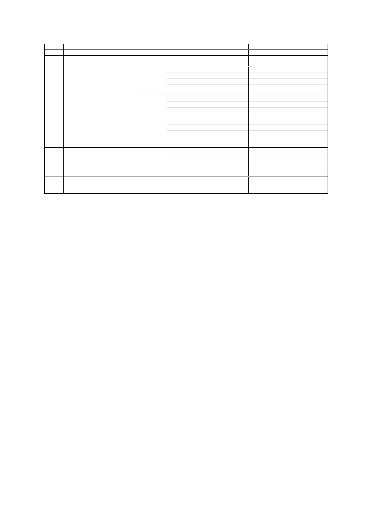
1-1: BACK CABINET (Refer to Fig. 1-1)
1.
Remove the 4 screws 1.
2.
Remove the screw 2 which are used for holding the
Back Cabinet.
3.
Remove the AC cord from the AC cord hook 3.
4.
Remove the Back Cabinet in the direction of arrow.
Front Cabinet
1
1-3: AV PCB/DVD BLOCK (Refer to Fig. 1-3)
Remove the screw 1.
1.
Remove the screw 2.
2.
Disconnect the following connectors:
3.
(CP301, CP401, CP302 and CP3800).
Remove the AV PCB/DVD Block in the direction of arrow.
4.
1
Front Cabinet
2
1
1
2
1
3
Back Cabinet
Fig. 1-1
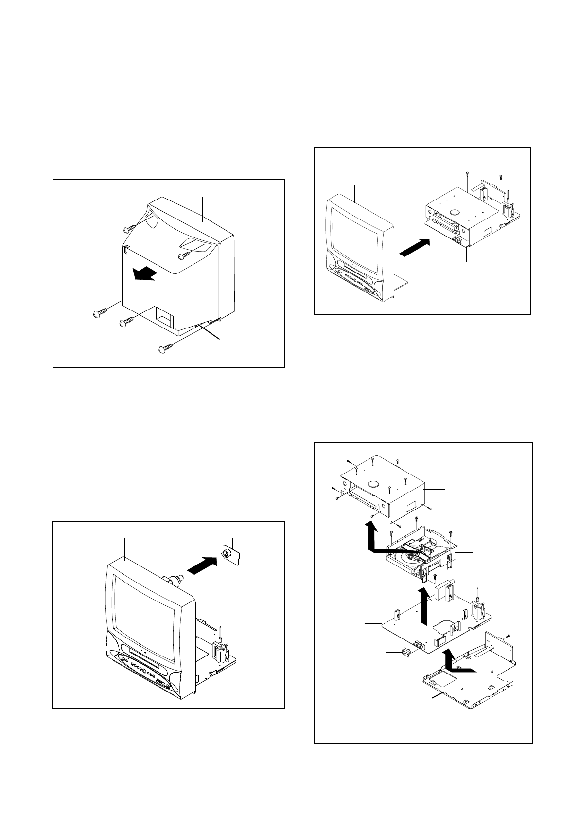
1-2: CRT PCB (Refer to Fig. 1-2)
CAUTION: BEFORE REMOVING THE ANODE CAP,
DISCHARGE ELECTRICITY BECAUSE IT
CONTAINS HIGH VOLTAGE.
BEFORE ATTEMPTING TO REMOVE OR
REPAIR ANY PCB, UNPLUG THE POWER
CORD FROM THE AC SOURCE.
1.
Remove the Anode Cap.
(Refer to REMOVAL OF ANODE CAP)
2.
Disconnect the following connector:
(CP801 and CP803B).
3.
Remove the CRT PCB in the direction of arrow.
Front Cabinet
CRT PCB
AV PCB/DVD Block
Fig. 1-3
1-4: DVD BLOCK (Refer to Fig. 1-4)
1.
Remove the 11 screws 1.
2.
Remove the Top Shield in the direction of arrow (A).
3.
Disconnect the following connectors:
(CP8001 and CP8002).
4.
Remove the 4 screws 2.
5.
Remove the DVD Block in the direction of arrow (B).
6.
Remove the screw 3.
7.
Remove the Jack Shield.
8.
Remove the AV PCB in the direction of arrow (C).
1
1
1
1
1
(A)
1
1
1
1
1
2
Top Shield
1
2
2
Fig. 1-2
B1-1
AV PCB
Jack Shield
DVD Block
2
(B)
3
(C)
Bottom Plate
Fig. 1-4
Page 14
DISASSEMBLY INSTRUCTIONS
1-5: DVD PCB/DVD DECK (Refer to Fig. 1-5)
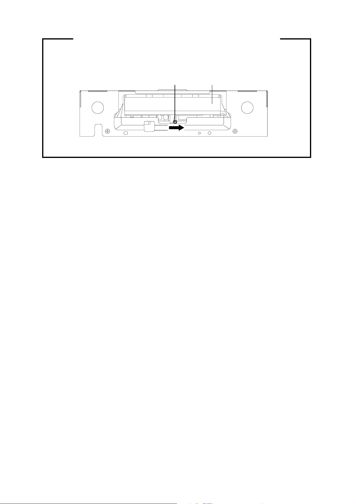
1.
Make the short circuit on the position as shown Fig. 1-5
using a soldering. If you remove the DVD Deck with no
soldering, the Laser may be damaged.
2.
Disconnect the following connectors:
(CP2601, CP2602 and CP2603).
3.
Remove the 4 screws 1.
4.
Remove the DVD Deck in the direction of arrow (A).
5.
Remove the 4 screws 2.
6.
Remove the DVD PCB in the direction of arrow (B).
Make the short circuit
using a soldering.
1
1
DVD Deck
1
DVD PCB
1
(A)
2
2
2
2
(B)
Pick Up PCB
Deck Angle
Fig. 1-5
NOTE
When the installation of the DVD Deck, remove all the
soldering on the short circuit position after the connection of
Pick Up PCB and DVD PCB connector.
B1-2
Page 15
DISASSEMBLY INSTRUCTIONS
2. REMOVAL OF DVD DECK PARTS
NOTE
1. Do not disassemble the DVD DECK PARTS except
listed parts here. Minute adjustments are needed if the
disassemble is done. If the repair is needed except
listed parts, replace the DVD MECHA ASS'Y.
2-1: TRAY (Refer to Fig. 2-1-A)
Set the Tray opened. (Refer to the DISC REMOVAL
1.
METHOD AT NO POWER SUPPLY)
Unlock the support 1 and remove the Tray.
2.
Main Frame Ass'y
Tray
NOTE
In case of the Tray installation, install them as the
1.
circled section of Fig. 2-1-B so that the each markers
are met.
1
Fig. 2-1-A
NOTE
In case of the Main Chassis Ass'y, install it from (1) to
1.
(6) in order. (Refer to Fig. 2-2-B)
Main Chassis Ass'y
Rack Loading
1
2
Move it to the direction
of the arrow.
Main Frame Ass'y
3
5
6
4
6
Check Lock
Fig. 2-2-B
2-3:
RACK LOADING/MAIN GEAR/ RACK LOADING
SPRING (Refer to Fig. 2-3)
Press down the catcher 1 and slide the Rack Loading.
1.
Remove the Rack Loading, Rack Loading Spring and
2.
Main Gear.
Remove the Rack Loading, Rack L Spring and Main
3.
Gear.
4
5
Tray
Main Frame Ass'y
Fig. 2-1-B
2-2: MAIN CHASSIS ASS'Y (Refer to Fig. 2-2-A)
Remove the Main Chassis Ass'y from the Insulator (R).
1.
Unlock the support 1.
2.
Remove the Main Chassis Ass'y.
3.
Insulator (R)
(Green)
Main Frame Ass'y
1
Rack Loading
Rack Loading Spring
Rack L Spring
1
2-4:
CLAMPER ASS'Y/INSULATOR(R)/LEVER SWITCH
Main Gear
Main Frame Ass'y
(Refer to Fig. 2-4-A)
Remove the screw 1.
1.
Remove the Lever Switch.
2.
Remove the 2 Insulator (R).
3.
Press the Clamper and rotate the Clamper Plate
4.
clockwise, then unlock the 3 supports 2.
Remove the Clamper Plate, Clamper Magnet and
5.
Clamper.
Clamper Plate
Clamper Magnet
Insulator (R)
(Green)
Insulator (R)
(Green)
Fig. 2-3
Main Chassis Ass'y
Fig. 2-2-A
B2-1
Lever Switch
Main Frame
2
2
1
Clamper
2
Fig. 2-4-A
Page 16
DISASSEMBLY INSTRUCTIONS
NOTE
1.
When installing the Clamper Magnet, install it with the
green face up.
2.
When installing the wire of the Lever Switch, install it
correctly as Fig. 2-4-B.
3.
When installing the Lever Switch, install it correctly as
Fig. 2-4-C.
4.
In case of the Lever Switch installation, hook the wire
on the Main Frame as shown Fig. 2-4-D.
Lever Switch
Red
White
Blue
From DVD PCB
Fig. 2-4-B
The Lever should be position
between A and B.
Rack Loading
AB
Main Chassis Ass'y
Traverse Holder
2-6: SWITCH PCB ASS'Y (Refer to Fig. 2-6-A)
Remove the screw 1.
1.
Remove the Switch PCB Ass'y.
2.
1
Switch PCB Ass'y
Main Chassis Ass'y
• Screw Torque: 4 ± 0.5kgf•cm
Fig. 2-5-B
Fig. 2-6-A
2-5:
TRAVERSE HOLDER/INSULATOR (F)
(Refer to Fig. 2-5-A)
Remove the Traverse Holder.
1.
Remove the 2 Insulator (F).
2.
Main Chassis Ass'y
Insulator (F)
(Black)
Traverse Holder
Fig. 2-4-C
Lever Switch
Fig. 2-4-D
NOTE
1. When installing the wire of the Switch PCB, install it
correctly as Fig. 2-6-B.
Switch PCB Ass'y
Black
From Relay PCB
White
Fig. 2-6-B
2-7: RACK FEED ASS'Y (Refer to Fig. 2-7-A)
Remove the screw 1.
1.
Remove the Rack Feed 1A Spring, Rack Feed 1A/2A
2.
and Rack Feed Lever.
1
Rack Feed 2A
Rack Feed 1A Spring
Rack Feed Lever
Rack Feed 1A
Main Chassis Ass'y
Insulator (F)
(Black)
Fig. 2-5-A
NOTE
1. After the installing of the Traverse Holder, check if the
wire is like Fig. 2-5-B.
B2-2
• Screw Torque: 3.5 ± 0.5kgf•cm
Fig. 2-7-A
Page 17
DISASSEMBLY INSTRUCTIONS
NOTE
1.2.After the assembly of the Rack Feed, check if the Rack
Feed 1/2 is moving smoothly. (Refer to Fig. 2-7-B)
In case of the Rack Feed Ass'y installation, install
correctly as Fig. 2-7-C.
Moving smoothly
Moving smoothly
Check the position of
the Rack Feed Lever.
Should not be engaged.
Fig. 2-7-B
Fig. 2-7-C
2-8: RELAY PCB ASS'Y (Refer to Fig. 3-8-A)
Remove the screw 1.
1.
Remove the Relay PCB Ass'y.
2.
Main Chassis Ass'y
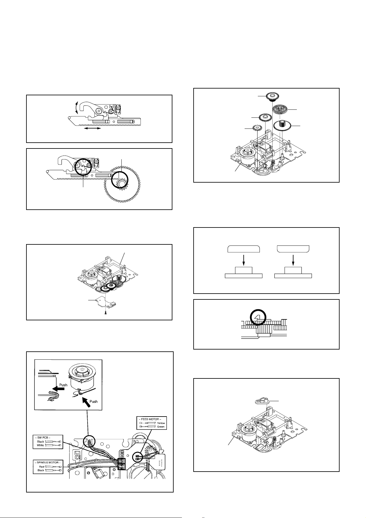
2-9: GEAR (Refer to Fig. 3-9-A)
Unlock the support 1.
1.
Remove the Middle Gear 1/2/3, Idler Gear and Feed
2.
Gear.
Middle Gear 2
Middle Gear 1
Middle Gear 3
Idler Gear
Main Chassis Ass'y
1
Feed Gear
Fig. 2-9-A
NOTE
1.2.In case of the Idler Gear installation, install correctly as
Fig. 2-9-B.
When installing the Middle Gear 2, check if the Middle
Gear 2 is locked correctly as Fig. 2-9-C.
[OK] [NG]
Idler Gear
Idler Gear
Relay PCB Ass'y
• Screw Torque: 4 ± 0.5kgf•cm
1
Fig. 2-8-A
NOTE
1. When installing the wire of the Relay PCB, install it
correctly as Fig. 2-8-B.
Idler Arm Idler Arm
Check Lock
Middle Gear 2
2-10: IDLER ARM 2 (Refer to Fig. 2-10-A)
Remove the Idler Arm 2.1.
Idler Arm 2
Main Chassis Ass'y
Fig. 2-9-B
Fig. 2-9-C
Fig. 2-8-B
Fig. 2-10-A
B2-3
Page 18
DISASSEMBLY INSTRUCTIONS
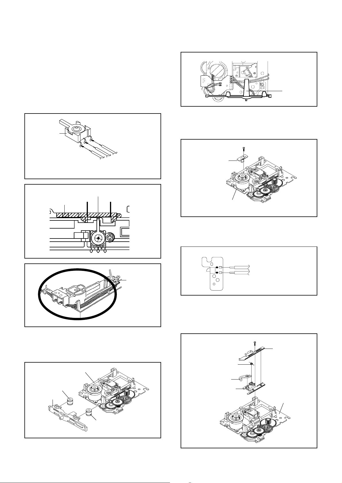
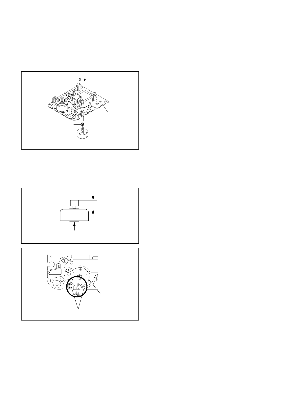
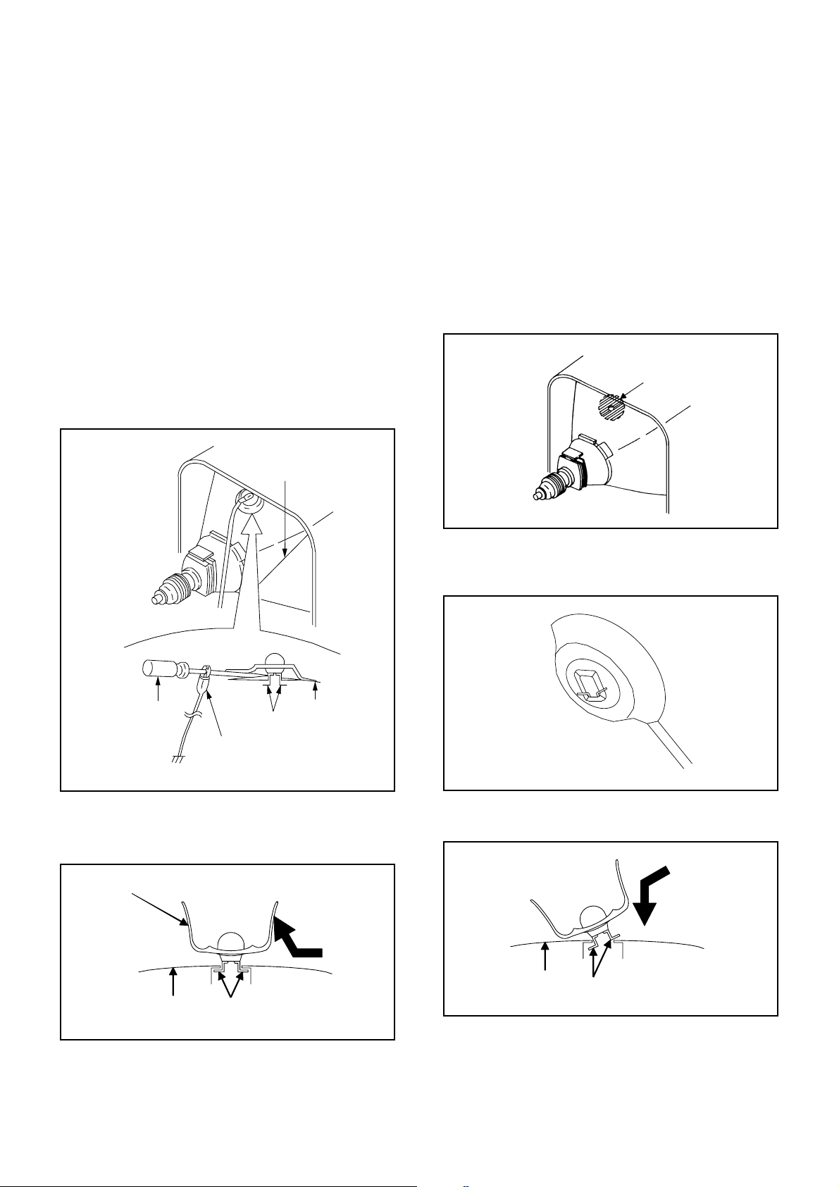
2-11: FEED MOTOR (Refer to Fig. 2-11-A)
Remove the 2 screws 1.
1.
Remove the Feed Motor.
2.
Remove the Motor Gear.
3.
1
1
Main Chassis Ass'y
Motor Gear
Feed Motor
• Screw Torque: 1 ± 0.5kgf•cm
Fig. 2-11-A
NOTE
1.2.In case of the Motor Gear installation, check if the value
of the Fig. 2-11-B is correct.
When installing the Feed Motor, check if the cable is
positioned as Fig. 2-11-C.
Motor Gear
Feed Motor
Safety surface for pressing
of the insert.
Main Chassis Ass'y
6.1 ± 0.1mm
Fig. 2-11-B
Pass the cable
between 2 pins.
Feed Motor
Fig. 2-11-C
B2-4
Page 19
DISASSEMBLY INSTRUCTIONS
3. REMOVAL OF ANODE CAP
Read the following NOTED items before starting work.
After turning the power off there might still be a potential
*
voltage that is very dangerous. When removing the
Anode Cap, make sure to discharge the Anode Cap's
potential voltage.
*
Do not use pliers to loosen or tighten the Anode Cap
terminal, this may cause the spring to be damaged.
REMOVAL
1. Follow the steps as follows to discharge the Anode Cap.
(Refer to Fig. 3-1.)
Connect one end of an Alligator Clip to the metal part of a
flat-blade screwdriver and the other end to ground.
While holding the plastic part of the insulated Screwdriver,
touch the support of the Anode with the tip of the
Screwdriver.
A cracking noise will be heard as the voltage is discharged.
GND on the CRT
3. After one side is removed, pull in the opposite direction
to remove the other.
NOTE
Take care not to damage the Rubber Cap.
INSTALLATION
1. Clean the spot where the cap was located with a small
amount of alcohol. (Refer to Fig. 3-3.)
NOTE
Confirm that there is no dirt, dust, etc. at the spot where
the cap was located.
Location of Anode Cap
Fig. 3-3
Screwdriver
Alligator Clip
GND on the CRT
Flip up the sides of the Rubber Cap in the direction of
2.
the arrow and remove one side of the support.
(Refer to Fig. 3-2.)
Rubber Cap
Support
CRT
Fig. 3-1
2.3.Arrange the wire of the Anode Cap and make sure the
wire is not twisted.
Turn over the Rubber Cap. (Refer to Fig. 3-4.)
Fig. 3-4
4. Insert one end of the Anode Support into the anode
button, then the other as shown in Fig. 3-5.
CRT
Support
Fig. 3-2
CRT
5.6.Confirm that the Support is securely connected.
Put on the Rubber Cap without moving any parts.
B3-1
Support
Fig. 3-5
Page 20
DISASSEMBLY INSTRUCTIONS
4.
REMOVAL AND INSTALLATION OF
FLAT PACKAGE IC
REMOVAL
Put the Masking Tape (cotton tape) around the Flat
1.
Package IC to protect other parts from any damage.
(Refer to Fig. 4-1.)
NOTE
Masking is carried out on all the parts located within
10 mm distance from IC leads.
When IC starts moving back and forth easily after
3.
desoldering completely, pickup the corner of the IC using
a tweezers and remove the IC by moving with the IC
desoldering machine. (Refer to Fig. 4-3.)
NOTE
Some ICs on the PCB are affixed with glue, so be
careful not to break or damage the foil of each IC
leads or solder lands under the IC when removing it.
Blower type IC
desoldering
machine
Masking Tape
(Cotton Tape)
Heat the IC leads using a blower type IC desoldering
2.
IC
machine. (Refer to Fig. 4-2.)
NOTE
Do not add the rotating and the back and forth
directions force on the IC, until IC can move back and
forth easily after desoldering the IC leads completely.
Blower type IC
desoldering machine
Fig. 4-1
Tweezers
IC
Peel off the Masking Tape.
4.
Absorb the solder left on the pattern using the Braided
5.
Shield Wire. (Refer to Fig. 4-4.)
NOTE
Do not move the Braided Shield Wire in the vertical
direction towards the IC pattern.
Fig. 4-3
Braided Shield Wire
Soldering Iron
IC
IC pattern
Fig. 4-4
Fig. 4-2
B4-1
Page 21
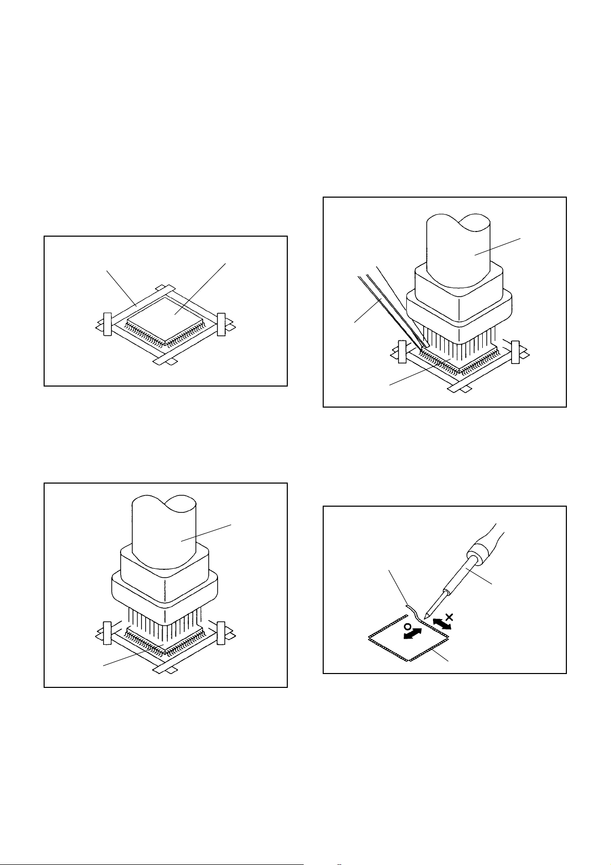
DISASSEMBLY INSTRUCTIONS
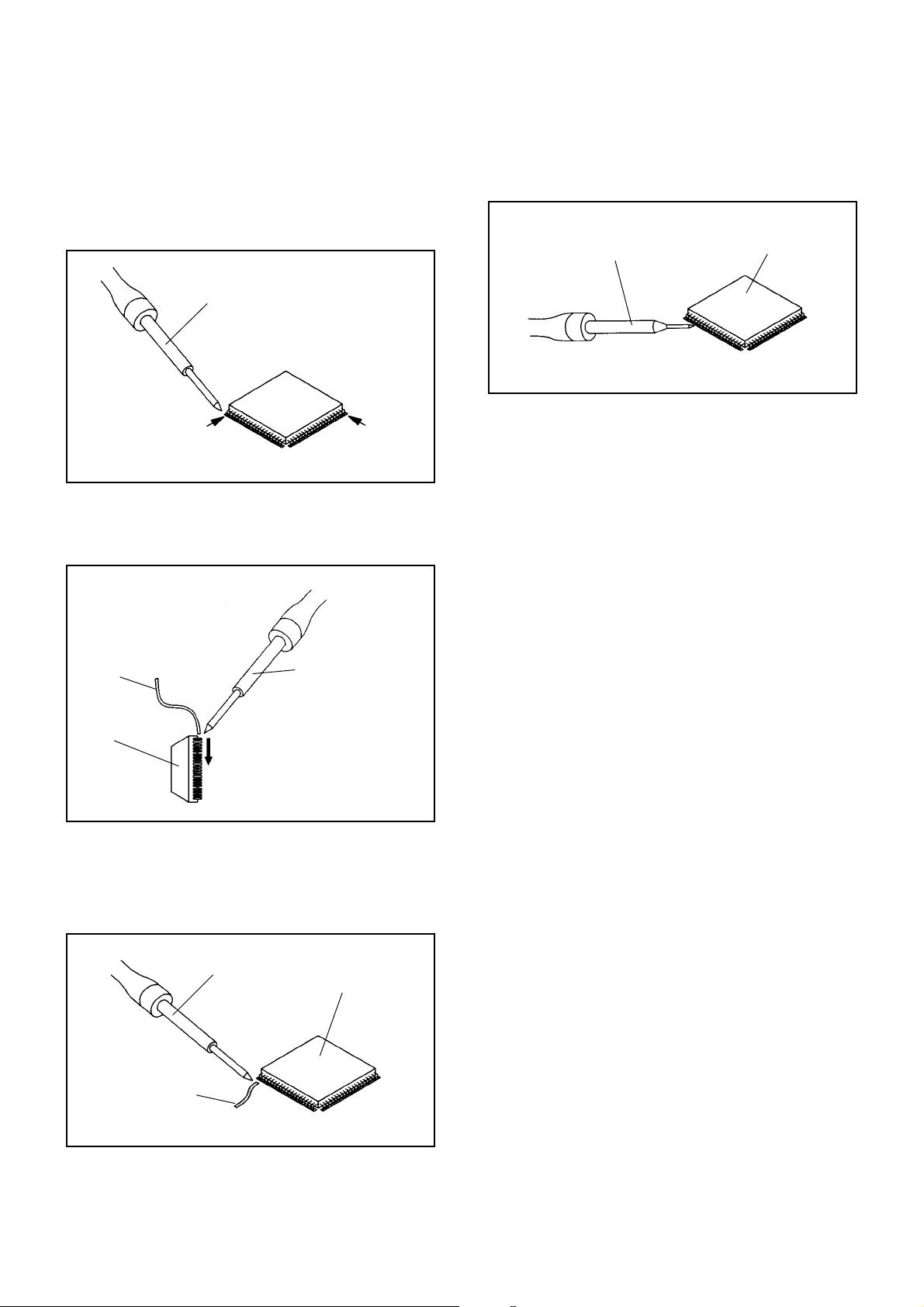
INSTALLATION
Take care of the polarity of new IC and then install the
1.
new IC fitting on the printed circuit pattern. Then solder
each lead on the diagonal positions of IC temporarily.
(Refer to Fig. 4-5.)
Soldering Iron
Solder temporarily
Supply the solder from the upper position of IC leads
2.
Solder temporarily
sliding to the lower position of the IC leads.
(Refer to Fig. 4-6.)
Fig. 4-5
When bridge-soldering between terminals and/or the
4.
soldering amount are not enough, resolder using a Thintip Soldering Iron. (Refer to Fig. 4-8.)
Thin-tip Soldering Iron
IC
Fig. 4-8
Finally, confirm the soldering status on four sides of the
5.
IC using a magnifying glass.
Confirm that no abnormality is found on the soldering
position and installation position of the parts around the
IC. If some abnormality is found, correct by resoldering.
NOTE
When the IC leads are bent during soldering and/or
repairing, do not repair the bending of leads. If the
bending of leads are repaired, the pattern may be
damaged. So, be always sure to replace the IC in this
case.
Soldering IronSolder
IC
Absorb the solder left on the lead using the Braided
3.
Supply soldering
from upper position
to lower position
Shield Wire. (Refer to Fig. 4-7.)
NOTE
Do not absorb the solder to excess.
Soldering Iron
IC
Braided Shield Wire
Fig. 4-6
Fig. 4-7
B4-2
Page 22
SER VICE MODE LIST
This unit provided with the following SERVICE MODES so you can repair, examine and adjust easily.
To enter to the SERVICE MODE function, press and hold both buttons simultaneously on the main unit and on the remote
control for more than a standard time (second).
Set Key
VOL. (-) MIN
VOL. (-) MIN 1
VOL. (-) MIN 4
VOL. (-) MIN 6
VOL. (-) MIN 9
STOP 7
STOP 9 3
0
Standard Time
(seconds)
1
1
1
1
3
OperationsRemocon Key
Releasing of V-CHIP PASSWORD.1
Initialization of the factory on TV.
NOTE:
Initialization of the factory on DVD.
NOTE:
POWER ON total hours are displayed on the screen.
Refer to the "PREVENTIVE CHECKS AND SERVICE INTERVALS"
(CONFIRMATION OF HOURS USED).
Can be checked of the INITIAL DATA of MEMORY IC.
Refer to the "WHEN REPLACING EEPROM (MEMORY) IC".
Display of the Adjustment MENU on the screen.
Refer to the "ELECTRICAL ADJUSTMENT" (On-Screen Display
Adjustment).
Releasing of PARENTAL LOCK.
Refer to the "PARENTAL CONTROL-RATING LEVEL"
NOTE: The function will only work without the setting of DVD disc at DVD
mode.
Tray cannot be opened.
Refer to the "TRAY LOCK".
NOTE: No indications on the screen when the Tray Lock is setting.
Do not use this for the normal servicing.
If you set a factory initialization, the memories are reset such as
the channel setting, and the POWER ON total hours.
Do not use this for the normal servicing.
The function will only work at the DVD stop mode.
CONFIRMATION OF HOURS USED
POWER ON total hours can be checked on the screen. Total hours are displayed in 16 system of notation.
NOTE: If you set a factory initialization, the total hours is reset to "0".
1.
Set the VOLUME to minimum.
2.
Press both VOL. DOWN button on the set and Channel
button (6) on the remote control for more than 2 second.
3.
After the confirmation of using hours, turn off the power.
C-1
ADDRESS DATA
INIT 00 06
CRT ON 0010
FIG. 1
Initial setting content of MEMORY IC.
POWER ON total hours.
= (16 x 16 x 16 x thousands digit value)
+ (16 x 16 x hundreds digit value)
+ (16 x tens digit value)
+ (ones digit value)
Page 23
WHEN REPLACING EEPROM (MEMORY) IC
If a service repair is undertaken where it has been required to change the MEMORY IC, the following steps should be taken to
ensure correct data settings while making reference to TABLE 1.
NOTE: No need setting for after INI 27.
+0 +1 +2 +3 +4 +5 +6 +7 +8 +9
06 0F 44 20 D0 35 30 25 15 50
50
30 50 04 15 77 23 50 20 77
10
0A 0D 10 12 14 16 18 1A --- ---
20 --- --- --- --- --- ---
Table 1
1.
Enter DATA SET mode by setting VOLUME to minimum.
2.
Press both VOL. DOWN button on the set and Channel button (6) on the remote control for more than 1 second.
ADDRESS and DATA should appear as FIG 1.
ADDRESS DATA
INIT 00 06
CRT ON 0010
FIG. 1
3.
ADDRESS is now selected and should "blink". Using the VOL. UP/DOWN button on the remote, step through the ADDRESS
until required ADDRESS to be changed is reached.
4.
Press ENTER to select DATA. When DATA is selected, it will "blink".
5.
Again, step through the DATA using VOL. UP/DOWN button until required DATA value has been selected.
6.
Pressing ENTER will take you back to ADDRESS for further selection if necessary.
7.
Repeat steps 3 to 6 until all data has been checked.
8.
When satisfied correct DATA has been entered, turn POWER off (return to STANDBY MODE) to finish DATA input.
+A
+B +C +D +E +FINI
01 00 C1 55 0F 4700
52 00 02 11 00 00
After the data input, set to the initializing of shipping.
9.
Turn POWER on.
10.
Press both VOL. DOWN button on the set and Channel button (1) on the remote control for more than 1 second.
11.
After the finishing of the initializing of shipping, the unit will turn off automatically.
The unit will now have the correct DATA for the new MEMORY IC.
C-2
Page 24
ELECTRICAL ADJUSTMENTS
1.
BEFORE MAKING ELECTRICAL
ADJUSTMENTS
Read and perform these adjustments when repairing the
circuits or replacing electrical parts or PCB assemblies.
CAUTION
•
Use an isolation transformer when performing any service
on this chassis.
•
Before removing the anode cap, discharge electricity
because it contains high voltage.
•
When removing a PCB or related component, after
unfastening or changing a wire, be sure to put the wire
back in its original position.
•
When you exchange IC and Transistor for a heat sink,
apply the silicon grease on the contact section of the heat
sink. Before applying new silicon grease, remove all the old
silicon grease. (Old grease may cause damages to the IC
and Transistor).
Prepare the following measurement tools for electrical
adjustments.
1. Oscilloscope
2. Digital Voltmeter
3. AC Voltmeter
4. Pattern Generator
5. Multi-Sound Signal Generator
On-Screen Display Adjustment
Set the VOLUME to minimum.
1.
Press the VOL. DOWN button on the set and the Channel
2.
button (9) on the remote control for more than 1 second
to appear the adjustment mode on the screen as shown
in Fig. 1-1.
Function
Step No.
01 OSD
12
NO.
FUNCTION
01
OSD H
02
OSD CONTRAST
03
CUT OFF
04
H POSITION
05
H BLK L
06
H BLK R
07
V SIZE
08
V POSITION
09
V LINEARITY
10
V S CORRECTION
11
V COMP
12
R CUT OFF
13
G CUT OFF
14
B CUT OFF
15
R DRIVE
16
G DRIVE
17
B DRIVE
18
BRIGHTNESS(CENT.)
19
BRIGHTNESS(MAX)
20
BRIGHTNESS(MIN)
21
CONTRAST(CENT.)
22
CONTRAST(MAX)
23
CONTRAST(MIN)
24
COLOR(CENT.)
25
COLOR(MAX)
26
COLOR(MIN)
27
TINT
28
SHARPNESS
29
SUB BIAS
30
BRI. AV(CENT.)
31
BRI. AV(MAX)
32
BRI. AV(MIN)
33
CONT. AV(CENT.)
34
CONT. AV(MAX)
35
CONT. AV(MIN)
36
COL. AV(CENT.)
37
COL. AV(MAX)
38
COL. AV(MIN)
39
TINT AV
40
SHARPNESS AV
FUNCTION
NO.
SUB BIAS
41
BRI. DVD(CENT.)
42
BRI. DVD(MAX)
43
BRI. DVD(MIN)
44
CONT. DVD(CENT.)
45
CONT. DVD(MAX)
46
CONT. DVD(MIN)
47
COL. DVD(CENT.)
48
COL. DVD(MAX)
49
COL. DVD(MIN)
50
TINT DVD
51
SHARPNESS DVD
52
SUB BIAS
53
BRI. GAME(CENT.)
54
BRI. GAME(MAX)
55
BRI. GAME(MIN)
56
CONT. GAME(CENT.)
57
CONT. GAME(MAX)
58
CONT. GAME(MIN)
59
SUB BIAS
60
TUNING V MUTE
61
POWER ON V MUTE
62
INPUT LEVEL
63
SEPARATION L
64
SEPARATION H
65
X-RAY TEST
66
H STOP
67
H FREQ
68
BAST/WEST DC
69
BAST/WEST AMP
70
BAST/WEST TILT
71
BAST/WEST COR, TOP
72
BAST/WEST COR, BOT
73
H SIZE COMP
74
H BLK L AV
75
H BLK R AV
76
Fig. 1-2
2. BASIC ADJUSTMENTS
2-1: CONSTANT VOLTAGE
1.
Set condition is AV MODE without signal.
2.
Using the remote control, set the brightness and
contrast to normal position.
3.
Connect the digital voltmeter to TP401.
4.
Adjust the VR3800 until the digital voltmeter is 135 ±0.5V.
Use the Channel UP/DOWN button or Channel button
3.
(1-0) on the remote control to select the options shown in
Fig. 1-2.
Press the MENU button on the remote control to end the
4.
adjustments.
Fig. 1-1
2-2: FOCUS
1.
2.
3.
2-3: CUT OFF
1.
2.
3.
4.
5.
6.
D-1
Receive the monoscope pattern.
Turn the Focus Volume fully counterclockwise once.
Adjust the Focus Volume until picture is distinct.
Adjust the unit to the following settings.
R CUT OFF=7F, G CUT OFF=7F, B CUT OFF=7F,
R DRIVE=3F, G DRIVE=07, B DRIVE=3F
Place the set with Aging Test for more than 15 minutes.
Set condition is AV MODE without signal.
Using the remote control, set the brightness and
contrast to normal position.
Activate the adjustment mode display of Fig. 1-1 and
press the channel button (03) on the remote control to
select "CUT OFF".
Adjust the Screen Volume until a dim raster is obtained.
Page 25

ELECTRICAL ADJUSTMENTS
2-4: WHITE BALANCE
NOTE: Adjust after performing CUT OFF adjustment.
1.
Place the set with Aging Test for more than 15 minutes.
2.
Receive the gray scale pattern from the Pattern
Generator.
3.
Using the remote control, set the brightness and contrast
to normal position.
4.
Activate the adjustment mode display of Fig. 1-1 and
press the channel button (16) on the remote control to
select "G DRV".
5.
Press the CH. UP/DOWN button on the remote control to
select the "R CUT OFF", "G CUT OFF", "B CUT OFF",
"R DRIVE" or "B DRIVE".
6.
Adjust the VOL. UP/DOWN button on the remote control
to whiten the R CUT OFF, G CUT OFF, B CUT OFF, R
DRIVE and B DRIV E at each step tone sections equally.
7.
Perform the above adjustments 5 and 6 until the white
color is looked like a white.
2-5: HORIZONTAL POSITION
1.
Receive the monoscope pattern.
2.
Using the remote control, set the brightness and contrast
to normal position.
3.
Activate the adjustment mode display of Fig. 1-1 and
press the channel button (04) on the remote control to
select "HPOSI".
4.
Press the VOL. UP/DOWN button on the remote control
until the SHIFT quantity of the OVER SCAN on right and
left becomes minimum.
2-6: VERTICAL POSITION
1.
Receive the monoscope pattern.
2.
Using the remote control, set the brightness and
contrast to normal position.
3.
Activate the adjustment mode display of Fig. 1-1 and
press the channel button (08) on the remote control to
select "VPOSI".
4.
Check the step No. V POSI is "02".
5.
Adjust the VR401 until the horizontal line becomes fit
to notch of the shadow mask.
2-7: VERTICAL SIZE
1.
Receive the monoscope pattern.
2.
Using the remote control, set the brightness and
contrast to normal position.
3.
Activate the adjustment mode display of Fig. 1-1 and
press the channel button (07) on the remote control to
select "VSIZE".
4.
Press the VOL. UP/DOWN button on the remote control
until the Up/Down OVER SCAN Quantity becomes equal
to the Right/Left OVER SCAN Quantity.
5.
Receive a broadcast and check if the picture is normal.
2-8: VERTICAL LINEARITY
NOTE:
1.
2.
3.
4.
2-9: SEPARATION L, H
Please do the method (1) or method (2) adjustment.
Method (1)
1.
2.
3.
4.
5.
6.
7.
Method (2)
1.
2.
3.
4.
5.
6.
7.
8.
9.
Adjust after performing adjustments in section 2-7.
After the adjustment of Vertical Linearity, reconfirm
the Vertical Position and Vertical Size adjustments.
Receive the monoscope pattern.
Using the remote control, set the brightness and
contrast to normal position.
Activate the adjustment mode display of Fig. 1-1 and
press the channel button (09) on the remote control to
select "VLIN".
Press the VOL. UP/DOWN button on the remote control
until the SHIFT quantity of the OVER SCAN on upside
and downside becomes minimum.
Set the multi-sound signal generator for each different
L-ch and R-ch frequency (Ex. L-ch=2KHz, R-ch=400Hz)
and receive the RF signal.
Connect the oscilloscope to the Audio Out Jack.
Press the AUDIO button on the remote control to set to
the stereo mode.
Activate the adjustment mode display of Fig. 1-1 and
press the channel button (64) on the remote control to
select "SEPAL".
Press the VOL. UP/DOWN button on the remote control
to adjust it until the audio output wave becomes a fine
sine wave.
Press the CH UP button 1 time to set to "SEPAH" mode.
Press the VOL. UP/DOWN button on the remote control
to adjust it until the audio output wave becomes a fine
sine wave.
Set the multi-sound signal generator L-ch=1KHz, R-ch
=Non input and receive the RF signal.
Connect the oscilloscope to the Audio Out Jack (R-ch).
Press the AUDIO button on the remote control to set to
the stereo mode.
Activate the adjustment mode display of Fig. 1-1 and
press the channel button (64) on the remote control to
select "SEPAL".
Press the VOL. UP/DOWN button on the remote control
to adjust it until the R-ch output becomes minimum.
Press the CH UP button 1 time to set to "SEPAH" mode.
Press the VOL. UP/DOWN button on the remote control
to adjust it until the R-ch output becomes minimum.
Set the multi-sound signal generator L-ch=Non input,
R-ch=1KHz and receive the RF signal.
Connect the oscilloscope to the Audio Out Jack (L-ch).
Then perform the above adjustments 3~7.
D-2
Page 26
ELECTRICAL ADJUSTMENTS
2-10: OSD POSITION
Activate the adjustment mode display of Fig. 1-1.
1.
Press the VOL. UP/DOWN button on the remote control
2.
until the difference of A and B becomes minimum.
(Refer to Fig. 2-1)
01 OSD
12
A
2-11: LEVEL
1.
Receive the VHF HIGH (70dB).
2.
Connect the AC voltmeter to pin 6 of CP101.
3.
Activate the adjustment mode display of Fig. 1-1 and
press the channel button (63) on the remote control to
select "LVL".
4.
Press the VOL. UP/DOWN button on the remote control
until the AC voltmeter is 75 ± 2mV.
2-12: BRIGHT CENTER
1.
Activate the adjustment mode display of Fig. 1-1 and
press the channel button (18) on the remote control to
select "BRTC".
2.
Press the VOL. UP/DOWN button on the remote control
until the white 10% is starting to be visible.
3.
Receive a broadcast and check if the picture is normal.
4.
Press the INPUT SELECT button on the remote control
to set to the AV mode.
5.
Activate the adjustment mode display of Fig. 1-1 and
press the channel button (30) on the remote control to
select "BRTCA".
6.
Press the VOL. UP/DOWN button on the remote control
until the white 10% is starting to be visible.
7.
Receive a broadcast and check if the picture is normal.
8.
Press the TV/DVD button on the remote control to set to
the DVD mode.
9.
Activate the adjustment mode display of Fig. 1-1 and
press the channel button (42) on the remote control to
select "BRTCD".
10.
Press the VOL. UP/DOWN button on the remote control
to set the same step numbers as the AV.
B
Fig. 2-1
2-13: TINT
1.
Receive the color bar pattern. (RF Input)
2.
Using the remote control, set the brightness, contrast,
color and tint to normal position.
3.
Connect the oscilloscope to TP024.
4.
Activate the adjustment mode display of Fig. 1-1 and
press the channel button (27) on the remote control to
select "TNTC".
5.
Press the VOL. UP/DOWN button on the remote control
until the section "A" becomes a straight line.
(Refer to Fig. 2-2)
6.
Receive the color bar pattern. (Audio Video Input)
7.
Press the INPUT SELECT button on the remote control
to set to the AV mode.
8.
Using the remote control, set the brightness, contrast,
color and tint to normal position.
9.
Connect the oscilloscope to TP024.
10.
Activate the adjustment mode display of Fig. 1-1 and
press the channel button (39) on the remote control to
select "TNTCA".
11.
Press the VOL. UP/DOWN button on the remote control
until the section "A" becomes a straight line.
(Refer to Fig. 2-2)
12.
Press the TV/DVD button on the remote control to set to
the DVD mode.
13.
Using the remote control, set the brightness, contrast,
color and tint to normal position.
14.
Connect the oscilloscope to TP024.
15.
Activate the adjustment mode display of Fig. 1-1 and
press the channel button (51) on the remote control to
select "TNTCD".
16.
Press the VOL. UP/DOWN button on the remote control
until the same step numbers as the AV.
"A"
Fig. 2-2
2-14: SHARPNESS
1.
Receive the monoscope pattern.
2.
Activate the adjustment mode display of Fig. 1-1 and
press the channel button (28) on the remote control to
select "SHARP".
3.
Check if the step No. SHARP is "18".
4.
Press the INPUT SELECT button on the remote control
to set to the AV mode.
5.
Activate the adjustment mode display of Fig. 1-1 and
press the channel button (40) on the remote control to
select "SHARPA".
6.
Check if the step No. SHARP is "10".
7.
Press the TV/DVD button on the remote control to set
to the DVD mode.
8.
Activate the adjustment mode display of Fig. 1-1 and
press the channel button (52) on the remote control to
select "SHARPD".
9.
Press the VOL. UP/DOWN button on the remote control
to set the same step numbers as the AV.
D-3
Page 27
ELECTRICAL ADJUSTMENTS
2-15: OSD CONTRAST 2-17: CONTRAST MAX
1.
Receive the monoscop pattern.
2.
Activate the adjustment mode display of Fig. 1-1 and
press the channel button (02) on the remote control to
select "OSDC".
3.
Check the step No. OSDC is "03".
2-16: COLOR CENTER
1.
Receive the color bar pattern. (RF Input)
2.
Using the remote control, set the brightness, contrast,
color and tint to normal position.
3.
Connect the oscilloscope to TP022.
4.
Activate the adjustment mode display of Fig. 1-1 and
press the channel button (24) on the remote control to
select "COLC".
5.
Adjust the VOLTS RANGE VARIABLE knob of the
oscilloscope until the range between white 100% and
0% is set to 4 scales on the screen of the oscilloscope.
6.
Press the VOL. UP/DOWN button on the remote control
until the red color level is adjusted to 110 ± 5% of the
white level. (Refer to Fig. 2-3)
7.
Receive the color bar pattern. (Audio Video Input)
8.
Press the INPUT SELECT button on the remote control
to set to the AV mode.
9.
Using the remote control, set the brightness, contrast,
color and tint to normal position.
10.
Activate the adjustment mode display of Fig. 1-1 and
press the channel button (36) on the remote control to
select "COLCA".
11.
Adjust the VOLTS RANGE VARIABLE knob of the
oscilloscope until the range between white 100% and
0% is set to 4 scales on the screen of the oscilloscope.
12.
Press the VOL. UP/DOWN button on the remote control
until the red color level is adjusted to 110 ± 5% of the
white level. (Refer to Fig. 2-3)
13.
Press the TV/DVD button on the remote control to set
to the DVD mode.
14.
Activate the adjustment mode display of Fig. 1-1 and
press the channel button (48) on the remote control to
select "COLCD".
15.
Press the VOL. UP/DOWN button on the remote control
to decrease the step numbers by 8 steps to the AV.
Activate the adjustment mode display of Fig. 1-1 and
1.
press the channel button (22) on the remote control to
select "CNTX".
Press the VOL. UP/DOWN button on the remote control
2.
until the contrast step No. becomes "5A"
Receive a broadcast and check if the picture is normal.
3.
Press the INPUT SELECT button on the remote control
4.
to set to the AV mode.
Activate the adjustment mode display of Fig. 1-1 and
5.
press the channel button (34) on the remote control to
select "CNTXA".
Press the VOL. UP/DOWN button on the remote control
6.
until the contrast step No. becomes "5A"
Receive a broadcast and check if the picture is normal.
7.
Press the TV/DVD button on the remote control to set to
8.
the DVD mode.
Activate the adjustment mode display of Fig. 1-1 and
9.
press the channel button (46) on the remote control to
select "CNTXD".
Press the VOL. UP/DOWN button on the remote control
10.
to set the same step numbers as the AV.
2-18: Confirmation of Fixed Value (Step No.)
Please check if the fixed values of the each adjustment
items are set correctly referring below.
NO.
FUNCTION
05
H BLK L
06
H BLK R
10
V S CORRECTION
11
V COMP
16
G DRIVE
19
BRIGHTNESS(MAX)
20
BRIGHTNESS(MIN)
21
CONTRAST(CENT.)
23
CONTRAST(MIN)
25
COLOR(MAX)
26
COLOR(MIN)
29
SUB BIAS
31
BRI. AV(MAX)
32
BRI. AV(MIN)
33
CONT. AV(CENT.)
35
CONT. AV(MIN)
37
COL. AV(MAX)
38
COL. AV(MIN)
41
SUB BIAS
43
BRI. DVD(MAX)
44
BRI. DVD(MIN)
45
CONT. DVD(CENT.)
STEP NO.
04
02
08
03
07
70
2A
40
10
70
10
00
70
2A
40
10
70
10
00
70
2A
40
CONT. DVD(MIN)
47
COL. DVD(MAX)
49
COL. DVD(MIN)
50
SUB BIAS
53
BRI. GAME(MAX)
55
BRI. GAME(MIN)
56
CONT. GAME(CENT.)
57
CONT. GAME(MIN)
59
SUB BIAS
60
TUNING V MUTE
61
POWER ON V MUTE
62
H FREQ
68
BAST/WEST DC
69
BAST/WEST AMP
70
BAST/WEST TILT
71
BAST/WEST COR, TOP
72
BAST/WEST COR, BOT
73
H SIZE COMP
74
H BLK L AV
75
H BLK R AV
76
FUNCTION
NO.
STEP NO.
10
70
10
00
70
2A
40
10
00
00
40
3F
00
00
00
00
00
00
07
05
White 0%
White 100%
100%
Red Level
Fig. 2-3
D-4
Page 28
ELECTRICAL ADJUSTMENTS
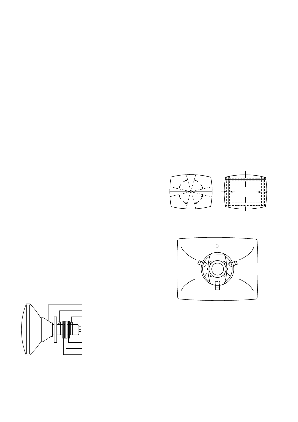
3.
PURITY AND CONVERGENCE
ADJUSTMENTS
NOTE
1.
Turn the unit on and let it warm up for at least 30
minutes before performing the following adjustments.
2.
Place the CRT surface facing east or west to reduce the
terrestrial magnetism.
3.
Turn ON the unit and demagnetize with a Degauss Coil.
3-1: STATIC CONVERGENCE (ROUGH ADJUSTMENT)
Tighten the screw for the magnet. Refer to the adjusted
1.
CRT for the position. (Refer to Fig. 3-1)
If the deflection yoke and magnet are in one body,
untighten the screw for the body.
Receive the green raster pattern from the color bar
2.
generator.
Slide the deflection yoke until it touches the funnel
3.
side of the CRT.
Adjust center of screen to green, with red and blue on the
4.
sides, using the pair of purity magnets.
Switch the color bar generator from the green raster
5.
pattern to the crosshatch pattern.
Combine red and blue of the 3 color crosshatch pattern
6.
on the center of the screen by adjusting the pair of
4 pole magnets.
Combine red/blue (magenta) and green by adjusting the
7.
pair of 6 pole magnets.
Adjust the crosshatch pattern to change to white
8.
by repeating steps 6 and 7.
3-2: PURITY
NOTE
Adjust after performing adjustments in section 3-1.
3-3: STATIC CONVERGENCE
NOTE
Adjust after performing adjustments in section 3-2.
1.
Receive the crosshatch pattern from the color bar
generator.
2.
Combine red and blue of the 3 color crosshatch pattern
on the center of the screen by adjusting the pair of
4 pole magnets.
3.
Combine red/blue (magenta) and green by adjusting the
pair of 6 pole magnets.
3-4: DYNAMIC CONVERGENCE
NOTE
Adjust after performing adjustments in section 3-3.
1.2.Adjust the differences around the screen by moving
the deflection yoke upward/downward and right/left.
(Refer to Fig. 3-2-a)
Insert three wedges between the deflection yoke and
CRT funnel to fix the deflection yoke.
(Refer to Fig. 3-2-b)
R G B
R
G
B
UPWARD/DOWNWARD SLANT RIGHT/LEFT SLANT
R
G
B
Fig. 3-2-a
R G B
1.
Receive the green raster pattern from color bar
generator.
2.
Adjust the pair of purity magnets to center the
color on the screen.
Adjust the pair of purity magnets so the color at the
ends are equally wide.
3.
Move the deflection yoke backward (to neck side)
slowly, and stop it at the position when the whole
screen is green.
4.
Confirm red and blue colors.
5.
Adjust the slant of the deflection yoke while watching the
screen, then tighten the fixing screw.
DEFLECTION YOKE
DEFLECTION YOKE SCREW
MAGNET SCREW
6 POLE MAGNETS
4 POLE MAGNETS
PURITY MAGNETS
Fig. 3-1
WEDGE
WEDGE
WEDGE
WEDGE POSITION
Fig. 3-2-b
D-5
Page 29
ELECTRICAL ADJUSTMENTS
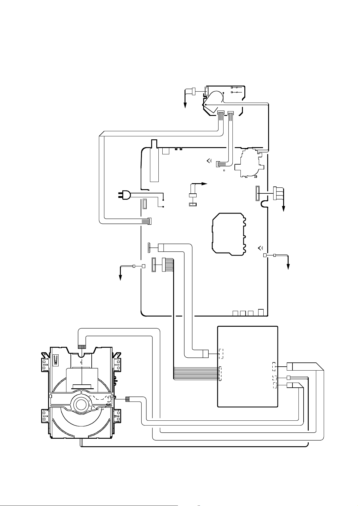
4. ELECTRICAL ADJUSTMENT PARTS LOCATION GUIDE (WIRING CONNECTION)
CRT PCB
CP801
CD805
CRT
J801
TP024
TP022
CP802B
CP803B
AC IN
SPEAKER
CD301
CP8002
CP301
TU001
CP101
CP802A
CP8001
J4201
S3802
S3801
CP3800
CD8501
VR3800
CP803A
CRT
AV PCB
TP401
J2202
FB401
CP401
J2203
VR401
CP302
J2204
CRT
CD302
SPEAKER
J2201
DVD DECK
D-6
CP8502
CD4002
CD2602
CD2601
CD2302
CP2601
CP2603
CP2602
DVD PCB
Page 30
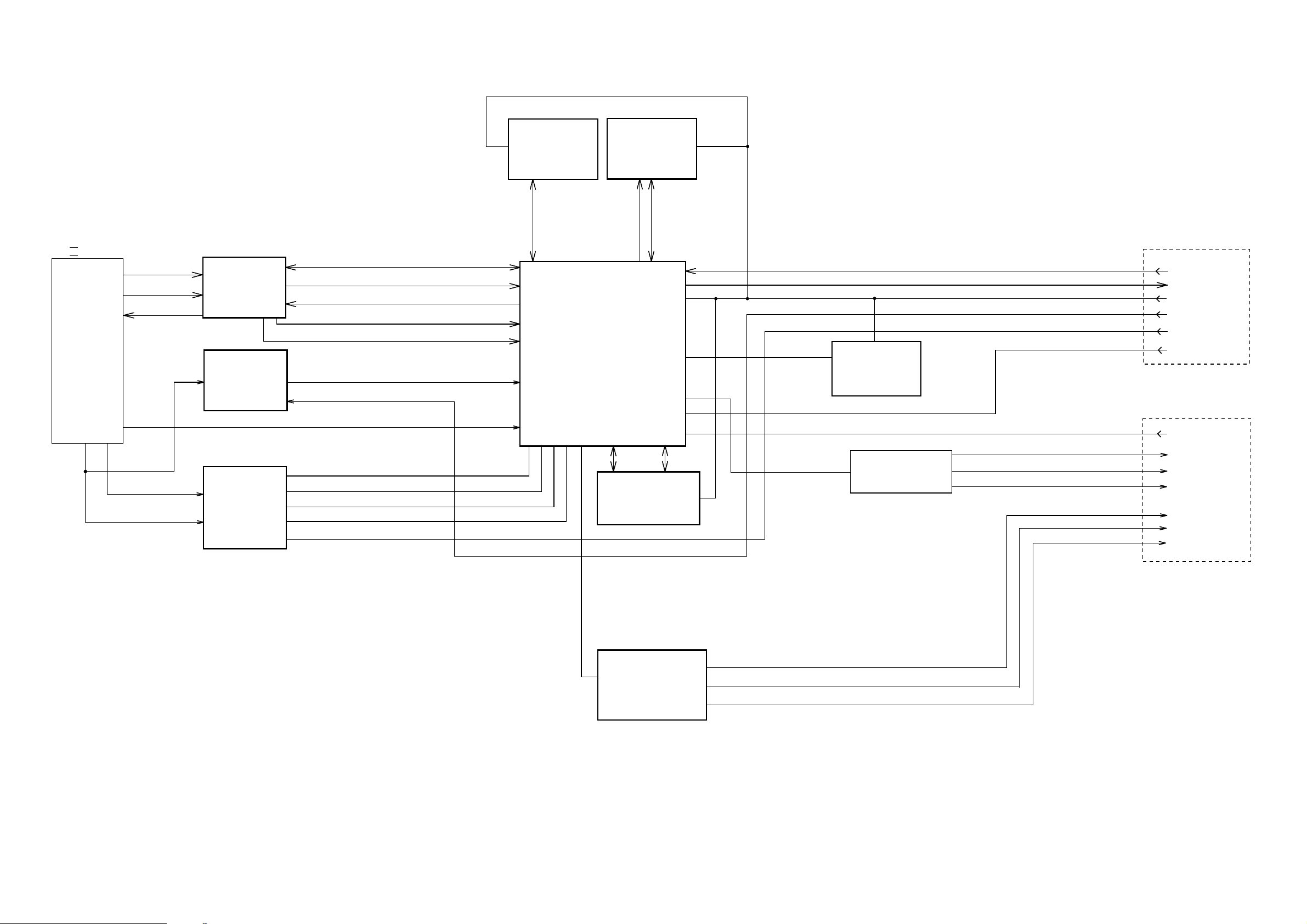
DVD BLOCK DIAGRAM
DVD LOADER
DM II
Pick up
Loading
Motor
Spindle/
Sled
Motor
A, B, C, D, E, F
RF
CD, DVD, LD
SPDL+/–
READ
CHANNEL
IC2601
ZR36708TQC
Dual OP-AMP
IC2602
BA10358F-E2
RFA_SDEN, DATA, SCLK
AAF_CE, FE, TE, PI
FNN, FNP
VBIASS0, S1
DEFECT, LINK, MIRR, LDON
SPDL_SENS
HOME, TIN SW, TOUT SW
8M FLASH
IC4007
SST39VF800A-
70-4C-EK-D
HA0~HA20,
HD0~HD15
MPEG/MICON/DSP
M12L64164A-7T
IC4001
ZR36762
64M SDRAM
IC4005
SDD0~SDD15
SDA0~SDA11
REG+1.8V
IC4003
PQ070XZ01ZP
VCR BLOCK
CD4002
TX
RX
P.CON+3.3V
P.CON+5V
P.CON+9V
SPDIF
CP8502
DVD RESET
TR+/–, FO+/–
SPDL+/–, SLED+/–
Motor Driver
IC2301
LA6560
SPINDLE, SLED_PWM
TRACK, FOCUS_DAC
ADC IN 5, 6, 7
S MUTE
2
I CDAT
EEPROM
IC4002
AT24C04N-10SI-2.7
ASDATA0
AMCLK
ABCLK
ALRCLK
STEREO DAC
IC8502
PCM1742KEG/2K
2
I CCLK
DAC B, C, D
DVD AUDIO L
DVD AUDIO R
VIDEO BUFFER
Q8502~Q8504
DVD VIDEO
Y
C
DVD AUDIO L
DVD AUDIO R
ZERO
E-1
E-2
Page 31

TV BLOCK DIAGRAM
FROM DVD BLOCK
DVD C
DVD Y
DVD_RESET
RX
TX
DVD_A_OUT_L
DVD_A_OUT_R
ZERO
SPDIF
POWER
ON/OFF
OPEN/CLOSE
STOP
PLAY
SKIP FF
SKIP REW
AMP
3
IC4201
NJM4580M
(TE1)
5
Q4203
MUTE
Q4201
DRIVER
*E
CH UP
CH DOWN
VOL UP
VOL DOWN
RESET
IC103 PST3231NR
*A
2
1
*A
X101
16MHz
18
17
31
32
MICON
IC101
OEC6079A
33
22
23
24
26
27
36
TU001
SCL
10
SDA
11
Q105
6 11 12
38 437
BUFFER
*B *C
57
56
55
R.OUT
59
1
7
R
Q4209~Q4212
L
MUTE SW
19 18
24
SOUND
23
DECORDER
2
3
IC902
AN5829S
22 21
*D
X601
3.579545MHz
40
30
51
50
42
35
14
15
16
45
23
25
G.OUT
B.OUT
Q405
H.DRIVE
119
Q406
3
V.OUT
IC401
AN5522
H.OUT
FB401
1
FBT
9
DY801
V801
CRT
3F987
F
S
HV
E-3
2
J4201
2
J2202
2
LV
J2203 J2204
2
R
Q305
Q302
BUFFER
BUFFER
Q301
MUTE
CHROMA
IC601 LA76319NM-MPB-E
9
SOUND AMP
IC302
6
AN7522N
8
SOUND+B
10
12
2
4
SPEAKER
SP351
SPEAKER
SP352
*A---AT+5.6V
*B---P.CON+9V
HEADPHONE
J2201
*C---CHROMA+5V
*D---P.CON+A5V
*E---P.CON+12V
E-4
Page 32

POWER BLOCK DIAGRAM
Q3003,
Q3004, Q3007
P.CON+3.3V OUT
P.CON+3.3V
AC IN
VR3800
+B ADJ.
L3800
DEGAUSS COIL
Q3800
FEED BACK
CONTROL
F3800
IC3800
PS2561L1-1-V(W)
FEED BACK
Q3803
POWER
D3808, D3809,
D3815, D3816
RECTIFIER
TRANSFORMER
SWITCHING
T3800
8
5
10
12
18
17
14
5V REG.
IC3001 KIA7805API
1
3
Q3008
DRIVE
5V REG.
IC3002 KIA7805API
3
1
Q3010
DRIVE
9V REG.
IC3005 KIA7809API
3
1
DVD_H
P.CON+D5V
AT+5.6V
SOUND+B
P.CON+5V
P.CON+D9V
E-5
FB401
Q3005
DRIVE
P.CON+9V
Q3000
DRIVE
P.CON+12V
Q3001
SW
POWER ON-H
+B
2
E-6
Page 33

PRINTED CIRCUIT BOARDS
W801
W808
W861
W802
R2621
CP2602
CP2603
R2650
R2651
R2619
CP2601
Q8502
C8506 C8509
C8505
L8502
C4084_1
B2605
C2647
Q2603
R2623
Q2604
R2647
W807
R2652
R2653
R2635
C2614
R2628
R2630
W877
W876
R8518 R8519 R8520
Q8503
C8512
C8508
C8511
L8503
C8507
C8504
C4036
C2641_1
R2620
C2639
R2624
R2622
Q2605
B2602
C2636
B2601
C2648
C2634
C2608_1
C2637
C2609
C2611
R2601
C2610
C2612
C2613
R2603
R2604
R2602
C2615
R2645
C2655
R2646
C2618
R2626
R2627
R2629
R2632
R2625
IC2602
C2649
B2603
DVD (TOP SIDE)
B8502
C8520
B8503
W879
R8509R8508R8507
Q8504
L8504
C8510
B4005
B4002
B4004
B4003
B4001
C4074
C2640_1
Q2602
R2617
R2654
R2618
D2601
R2615
C2638
Q2601
C2603
17
IC2601
33
C2623
C2617
R2607
R2608
R2609
R2649
R2611
R2631
C2644_1
C2645
C2643_1
C2642
B2604
VMC319A
C4038
R4039
R4038
R4037
W831
C4067_1
C4072
C4071_1
C4076
C4073
C4068_1
C4070_1
W833
C4069_1
C4088
R4043
C4089
C4090R4044
R2616
W806
C2604
C2605
C2606
C2607
1
49
C2616
R2643
C2622
R2610
R2605
R2613
C2646_1
R2648
R4005
R4004
R4003
R4002
R4001
R4017
C4007
C4006
C4075
C4005
C4085
C4086
C4004
C4003
W832
C4002
R4056
R4052
C4001
W857
R4051
R4049
R4050
C2635
C2626
C2625
C2624
R4022
C2627
C2629
C2628
C2633
R2614
C2632
C2654
R2644
C2619
C2620
C2621
R4057
R2303 C2302
C2303
R2612
C2660
R2304
C2659
C2308
C2658
C2307
C2657
W855
R4016
R4045
R4036
R4018
X4001
C4035
R4012 R4042
C4081
C4079
C4027
C4028
C4096
C4032
C4033
C4029
IC4001
1 53
C4010
C4008
R4046
C4013
R4061
R4060
R4041
W875
R2310
R2314
C2301
R2309_1
IC2301
HS2301
R2328
C2306
C2311
R2331_1
C8518
C8521_2
R4020
R4019
R4047
R4024
C4030
C4031
C8519_1
C8517_2
IC8502
R4027
R4026
R4021
C4098
R4053
R4058
R4025
R4014
C4025
B4010
105157
C4024
C4023
C4022
R4008
R4059
C4020
C4019
C4017
IC4007
C4018
C4016
C4078_1C4083_1
C4064
C4062
C4063_1
W862
R2301
R2306
R2305
R2307
R2308
R2316
R2321
R2319
R2322
R2326
R2324
R2327 C2309
C2312
R2337
C4014
W882
R2325
R2330
W878
C8514_1
W872
C8513_1
W860
R4054
R4031
R4035
C4050
C4046
C4047
C4077
C4051_1
R4040
R2313
R2312
W863
R2318
W864
C2305
R2334
R8515
R8514
C4026
C4094
C4093
R4064
C4043
B4008
R4033
C4040
L4001
R4013
C4009_1
R4032
C4012
C4080
W871
C8522
CP8502
W874
W873
C4066
C4065
B4009
C4099
C4092
D4001
R4011
CD4002
C4097
W805
C4042
C4015
R4034
IC4003
IC4002
C4037
C4045
C4041
IC4005
R4048
C4052_1
C4082
B4006
C4091
W854
Q4004
C4095C4039
B4007
C4011_1
C2304
R2344
R2345
C2310
VMC319A
DVD (BOTTOM SIDE)
F-1
F-2
Page 34

PRINTED CIRCUIT BOARDS
AV/CRT (INSERTED PARTS)
SOLDER SIDE
J2201
J2204
J2203
J2202
SW2221
SW2223
SW2217
SW2219
SW2216
SW2214
SW2218
SW2220
W204
SW2215
R2226
W825
W223
SW2213
OS2202
R
W
Y
D2201
W164
W163
W180
R2201
R2202
W221
C4275
W168
W167
W166
W165
W190
W189
R2225
W207
W205
C2201
W208
W834
W833
R909
W217
R101
D107
W222
C2204
R346
R323
W815
W844
W213
W173
W172
W171
C932
C101_1
W206
W225
W169
C936
W203
W202
W201
W200
W194
W193
W192
D101
W191
D105
W185
C907
D103
C328
W184
C931
W210
C2205
C110_1
W188
W209
W183
C928_1
R911
W216
C103
W212
C926
R190
W812
IC199
W220
W174
C347
W215
W211
C925
R912
W814
C921
W199
W804
R301
W179
W198
IC101
W214
C3017
W219
C346
R303
W182
C941
C410_1
W863
X101
D102
R125
W224
W218
W181
W175
W195
W805
C119_1
D3009
W153
IC302
W170
W108
C943
C945
W120
W197
Q3003
HS3001
W092
C920
W140
C3007
L3000
W097
L904
L101
W103
D106
W130
W098
W115
W138
W137
R3014
W122
W111
W837
R159
W135
W128
C3025
W093
W105
W096
C922
W819
C3005
W803
W121
W109
D3007
W131
W150
C312
L902
W156
W119
W110
W133
CP301
HS301
W813
W118
W147
W143
W139
W132
W152
C313
W123
W112
W142
R4251
R4252
CP8001
B301
W126
W114
W113
S802X
W094
W827
W832
CP302
W091
W124
W125
C4227
C633
R4240
W151
W090
W107
C624
W146
D416
W145
W159
W158
W148
R630
C4234
C407
C405
C628
W141
C4203
R4234
W160
C3012
W149
X601
W144
L4201
R416
R414
C602
C4231
VR401
R421
Q806
R4235
C4232
C4229
CP8002
R418
S002X
R805
R803
R807
L801
C626
C4230
W084
R407
D803
C604
W069
W083
W043
R806_1
Q804
C622
C603
C4217
W081
R413
W916
TP024
TP022
TP023
CP803B
L602
W052
W045
W064
W061
W080
R411
D801
C619
S002Y
S001X
Q805
R618
C606
R4218
C4206
W082
D401
W042
R802_1
R616
C609
C4214
W085
W044
C406
HS401_1
CP806_1
C802
D802
W054
C612
C611
W075
CP802B
W058
L601
R4219
C4207
W056
R627
R622
W046
W067
D603
W843
W057
R3019
W087
IC401
R613
R612
W077
W076
W074
W073
W072
C3014_1
D403
R3007
W063
R603
R3009
W088
W078
W050
W047
W065
W060
W055
D409
W089
D404
J801_1
W053
W049
R3003
R3004
W071
C605
C3028_1
W079
CP802A
W051
D3003
W041
R804
R3002
R3006
R3018
R3830
W066
R614
R467
W914
Q3000
C3001
W062
W012
C3023_2
Q3004
R3010
W031
C3015_1
C434_1
R412
W059
W040
C634
S802Y
W015
W826
R402
CP801
W023
R424
W029
L3001
W039
C421
W011
W028
S001Y
W038
W010
C3020
C3820
C3827
R3806
W037
W033
D405
W009
W020
D3803
D3005
W018
IC3002
S3802
W036
W014
W013
Q405
C417
Q3005
Q3009
W030
C3013_1
W025
CP3800
PH3800
C3801
W035
W032
W841
C3006
IC3005
L3801_1
R3803
CP101
T401
R3005
W017
C3030
W024
TH3800_2
S3801
W226
C429
R419
D3008
IC3001
D411
R417
C428
R460
C418
R456
Q3006
Q3008
C3021
D3823
C3816
PH3801
5V125V
C3026
R3001
W016
Q3010
D3006
W021
D3826
D3805
W026
R3817
W808
Q406
W019
W851
CP401
C423
R444
W022
C3815
F3800
R401
D3802
D3817
D3816
R447
D3831
C403
R3829
C3818
L401
HS402
R3813
D3815
C3812
D3808
C3810
FH3801FH3800
B401
D406
C422
D408
R405
R404
D3828
D3809
W001
W004
Q3802
RISK OF FIRE - REPLACE AS MARKED .
W828
W034
R4205
R003
W818
W838
R3828
R3826
R3802
D3821
D3810
C3814
D3804
R004
W810
R3827
W007
R3801
C3807
R3812
C3808
L001
C3826
R3816
R453
R442
T3800
B3800
R3821
C006_1
TP401
W006
D3811
FB401_1
C430
CP803A
D3820
W005
Q3803
HS3800
D3807
R3822
C4204_1
TP402
W003
C3811
TU001
D413
R445
L4202
C431
VR3800
D3830
W008
TP403
D3819
R3825
D410
D3827
D3801
R3805
R3804
D3806
W802
R450_1
C402
R423
D402
D3818
J4201
W002
R3800
D3822
C3822
R3833
IC3800
B4201
C439
W836
R3831
Q3800
C432_1
R430
C3823
W820
F-3
CD3800
L3803
F-4
Page 35

PRINTED CIRCUIT BOARDS
AV/CRT (CHIP MOUNTED PARTS)
SOLDER SIDE
C3809
C4224
R4216
R4221
C3805
Q4201
C4215
R4241R4210
R4242
C4205
C002
C001
C3806
R634
Q602
Q3007
Q3001
Q605
R4211
C614
C4210
R4212
R605
Q601
R4202
R4213
C617
R615
R4223
C608
R617
C4212
R4208
IC4201
C4225
C607
R607
R611
C618
C620
R628
R610
R4224
C4226
C4222
R608
R609
C613
R619
R4201
C4220
R4228
C621
R4229
R4231
C4216
R4232
17
C601
W809
R4230
R4233
R602
1
IC601
33
R624
Q4209
Q4203
49
C630
R4238
R4209
C629
R625
R4239
Q4210
C625
R626
Q4212
R4243
C627
Q4211
C4233
C3003
C631
C303
C632
R4237
R4236
C305
W849
C3002
R157
R145
C3004
R141
R142
R149
R144
C111
R109
Q101
R119
R160
R148
R106
W857
C127
C129
R140
C128
R120
Q105
R134
R114
C109
C106
W856
R122
R4227
C117
R132
C104
C124
R126
R113
C108
R147
R115
C102
C107
R143
IC103
R110
R127
R103
Q2201
R123
R121
R2214
R2216
R2219
R2217
R2215
R2218
R2220
W852
W850
R420
C810
R816
R808
C811
R813
R801
R809
C809
R815
C304
C302
R302
C331
R311
C307
C944
Q302
C348
R305
C323
R308
R307
W823
R306
R910
C306
W842
Q305
R310
IC902
C310
R304
R309
C933
C929
Q301
C935
C934
R908
C938
C937
R913
C939
R326
R2221
C2202
C2203
C4266
C4274
F-5
F-6
Page 36

8
7
FROM/TO MEMORY
6
5
4
3
2
1
ABC D E F GH
MPEG/MICON SCHEMATIC DIAGRAM
(DVD PCB)
C4038
0.01 B
4.7K
DUPTD1
DUPRD1
DUPTD0
DUPRD0
P.CON+5V
4.7K
R4036
R4037 4.7K
R4038 4.7K
R4039 4.7K
D_GND
P.CON+3.3V
HA0
HA1 AAF_PI
HA2 VR_SEL
HA3 FNN
HA4 FNP
HA5
HA6 VBIASS1
HA7 DEFECT
HA8 LINK
HA9 MIRR
HA10
HA11 SMUTE
HA12 TRACK_DAC
HA13 FOCUS_DAC
HA14 SPINDLE_PWM
HA15
HA16 TRACK_PWM
HA17 FOCUS_PWM
HA18 P.CON+A5V
HA19 P.CON+3.3V
HA20
HD0 P.CON+5V
HD1 ADCIN_7
HD2 ADCIN_6
HD3 ADCIN_5
HD4
HD5
HD6
HD7
HD8
HD9
HD10
HD11
HD12
HD13
HD14
HD15
MEMCS0
RD
WR
SD_A0
SD_A1
SD_A2
SD_A3
SD_A4
SD_A5
SD_A6
SD_A7
SD_A8
SD_A9
SD_A10
SD_A11
SD_D0
SD_D1
SD_D2
SD_D3
SD_D4
SD_D5
SD_D6
SD_D7
SD_D8
SD_D9
SD_D10
SD_D11
SD_D12
SD_D13
SD_D14
SD_D15
RAMCS0#
RAMCS1#
RAMRAS#
RAMCAS#
SD_BA0
RAMDQM
RAMWE#
RAMCLK
NC
BOOTSEL2 BOOTSEL1
C4008 0.1 F
HA15 DUPTD0
HA16 DUPRD0
HA14
HA13 VR_SEL
HA12 TRAY_OPEN
HD15 TOUT_SW
HA11 TRAY_CLOSE
HD7 TIN_SW
HA10
HD14
HA9
HD6
HA8
HD13
HD5
HA20 HOME HOME
C4010 0.1
HD12
WR DJTDO ML
HD4 DJTDI MC DUPTD1
C4013 0.1 F
HD11 ICETCK
HD3 ICETDO
HA19 ICETDI
HD10
HA18 I2CDAT
HD2 I2CDAT
HA17
HD9 I2CCLK
HA7
HD1
HA6
HD8 IAMCLK AMCLK
HA5
HD0 IALRCLK ALRCLK
HA4
RD ASDATA0
HA3 ASDATA1
HA2 ASDATA2 DUPRD1
MEMCS0 SPDIF
HA1
HA0
R4053
C4014 0.1 F
C4016 0.1 F
C4017 0.1 F
C4077
0.1 F
1K
F
C4078_1
NC
1006.3V KA
R4054
1K
R4046
NC
FPCRX
3.3
3.3
3.3
3.0
3.0
3.0
3.3
3.3
0.5
2.6
1.9
2.1
2.0
3.3
0.6
3.3
2.6
1.8
2.7
2.9
0.5
0.6
0.6
2.7
2.7
0.6
0.4
5.5
3.3
0.4
3.3
3.1
3.1
3.2
3.3
3.3
0
0
0
0
0
0
0
0
0
0
0
0
0
0
0
0
MIRR
SPDL_SENS
4.7K
R4049 4.7K
R4050
W857
FPCCLK
FPCTX
0.7
3.3
3.3
4.3
110
SSCRXD
MEMCS(1)
3
VDDP
4
MEMAD(15)
5
MEMAD(16)
MEMAD(14)
MEMAD(13)
MEMAD(12)
MEMDA(15)
MEMAD(11)
MEMDA(7)
111213141516171819 22021222324
GNDP
MEMAD(10)
MEMDA(14)
MEMAD(9)
MEMDA(6)
MEMAD(8)
MEMDA(13)
MEMDA(5)
MEMAD(20)
VDDP
MEMDA(12)
MEMWR#
MEMDA(4)
VDDC
2526272829
MEMDA(11)
MEMDA(3)
MEMAD(19)
GNDC
MEMDA(10)
30313233343536373839
MEMAD(18)
GNDP
MEMDA(2)
MEMAD(17)
MEMDA(9)
MEMAD(7)
MEMDA(1)
MEMAD(6)
MEMDA(8)
MEMAD(5)
40414243444546474849
VDDP
MEMDA(0)
MEMAD(4)
MEMRD#
MEMAD(3)
MEMAD(2)
MEMCS(0)#
MEMAD(1)
MEMAD(0)
GNDP
50
VDD-IP
5152
VDDP
53 545556 57 58 59660 61 62 63 64 65 66 67 68 69770 71 72 73 74 75 76 77 78 79880 81 82 83 84 85 86 87 88 89990 91 92 93 94 95 96 97 98 99
0.9
0.3
1.001.0
SD_A4
SD_A3
SD_A5
SD_A2
4.7K
R4051
C4001 0.1 F
FPCSTRB
3.3
VDDP
ICGPCI/O(7)
RAMADD(6)
VDDP
3.301.0
C4018 0.1 F
SD_A6
DEFECT
RFA_SDEN
RFA_DATA
RFA_SCLK
100
R4052 4.7K
R4057 100
R4056
C4002 0.1 F
IRRCV
3.30003.303.3
GNDP
VDDPWM
DEFECT
PWMCO(6)
PWMCO(5)
ICGPCI/O(6)
PWMCO(4)
208
SSCTXD
207
SSCCLK
SPINDLEPULSE
206
SLEDPULSE 157
205
W832
S_GND
2.903.3
GNDPWM
C4003 0.1 F
NC
NC
1.8
2.9
VDDC
PWMCO(2)
PWMCO(3)
SLED_PWM
R4060 1K
GNDC
PWMCO(1)
SPINDLE_PWM
AFE_GND
R4061 3.3K
NC
NC
PWMCO(0)
PWMACT(0)
PWMACT(1)
VBIASS1
VBIASS0
1.7
1.10000.701.5
VBIASS1
GNDAFES
VBIASS0
MPEG/MICON/DSP IC
RAMADD(4)
53
54
RAMADD(3)
55
RAMADD(5)
56
RAMADD(2)
RAMWE#
RAMADD(1)
RAMADD(7)
0.200.2
SD_A1
SD_A7
SD_A0
RAMADD(0)
GNDP
RAMADD(8)
SD_A8
VDDC
1.8
C4019 0.1 F
1.900.2
SD_A10
RAMADD(10)
RAMADD(9)
GNDC
3.303.1
C4020 0.1 F
SD_A9
RAMADD(11)
RAMBA(0)
VDDP
RAMCS(0)# RAMBA(1)
0.503.1
SD_A11
RAMCS0#
SD_BA0
GNDP
RAMCS(1)#
RAMCS1#
RAMCAS#
RAMRAS#
0.2
3.2
RAMRAS#
RAMCAS#
VDDP
3.3
3.2
RAMWE#
AAF_PI
AAF_TE
1.8
1.6
ADCIN(0)
IC4001
ZR36762
RAMDQM
0
0
R4059 47
RAMDQM
AAF_FE
AAF_CE
ADCIN(2)
ADCIN(1)
GNDPCLK
PCLK
1.6
3.3
C4022 0.1 F
R4008
RAMCLK
LINK
001.7
ADCIN(4)
ADCIN(3)
VDDPCLK
RAMDAT(8)
2.101.3
R4064 47
100
SD_D8
ADCIN_5
R4044 10K
1.6
ADCIN(5)
GNDP
NOTE:THE DC VOLTAGE EACH PART WAS
DIGITAL AUDIO SIGNAL(PB)
FNN
ADCIN_7
C4086
C4088
0.01 B
C4089
R4022 10K
0.01 B
C4090
0.01 B
C4004 0.1 F
1.7
VDDAFES
ADCIN(7)
RAMDAT(9)
RAMDAT(6)
0.8
0.8
SD_D9
SD_D6
0.001 B
RFINN
1.203.3
GNDAFERF
VDDP
3.3
1.7
C4023 0.1 F
SD_D10
FNP
C4085 0.001 B
RFINP
C4005 0.1 F
1.2
RFINP
RFINN
VDDAFERF
RAMDAT(10)
RAMDAT(5)
RAMDAT(11)
1.3
0.500.9
SD_D11
SD_D5
TRACK_DAC
C4006 0.1 F
3.3
0.803.3
VDDDACS
GNDDACDS
DACDRIVE(1)
160
VDDDAC
159
CVBS/C
158
CVBS/G/Y
GNDDACD
100
RAMDAT(14)
101
GNDP
102
RAMDAT(1)
103
RAMDAT(15)
104
RAMDAT(0)
GNDP
VDDC
RAMDAT(4)
1.8
C4024 0.1 F
SD_D4
FOCUS_DAC
47K
R4017
W833
0.9
GNDDACPS
DACDRIVE(0)
GNDC
RAMDAT(12)
1.400.5
SD_D12
SD_D3
000
GNDDACBS2
RAMDAAT(3)
3.3
C4025 0.1 F
ADCIN_6
R4043 10K
1.5
ADCIN(6)
RAMDAT(7)
SD_D7
MEASURED WITH THE DIGITAL TESTER
DURING PLAYBACK.
DAC_VIDEO_C
R4001 820 +-1%
1.2
1.2
RSET
GNDDACP
VDDP
RAMDAT(13)
2.0
0.4
SD_D13
SD_D2
DAC_VIDEO_B
C4007 0.1 F
3.3
1.1
C/B/U
Y/R/V
IDGPCI/O(3)
GPCI/O(34)
ICGPCI/O(5)
GPCI/O(33)
ICGPCI/O(4)
GPCI/O(32)
IDGPCI/O(2)
GPCI/O(31)
IDGPCI/O(0)
ICGPCI/O(0)
GPCI/O(20)
RAMDAT(2)
101102 103104
100
1.500.8
SD_D14
DAC_VIDEO_D
R4002 75 +-1%
R4003 75 +-1%
R4004 75 +-1%
R4005 75 +-1%
DAC_VIDEO_A
0
1.1
1.2
157158159160161162163164165166167168169170171172173174175176177178179180181182183184185186187188189190191192193194195196197198199200201202203204205206207208
DUPTD1
DUPRD1
VDD-IP
DUPTD0
DUPRD0
GNDP
VDDP
GCLKA
GCLKP
XO
VDDA
RESET#
GNDA
VID(0)
VID(1)
VID(2)
VID(3)
V SW
D1 2
D1 1
VID(7)
VDDP
STBY-L
GNDP
HSYNC
VDDC
VSYNC
GNDC
AIN
VDDP-A2
AMCLK
GNDP-A2
ABCLK
ALRCLK
GPAI/O
AOUT(0)
AOUT(1)
AOUT(2)
SPDIF
GNDP
VDDP
1.2
1.5
SD_D15
SD_D1
SD_D0
V_GND
GND
W831
476.3V KA
476.3V KA
C4068_1
C4067_1
+1.8V
+3.3V
3.3
5.1
3.3
3.3
5.0
0
3.3
0
3.3
0
0
3.1
3.3
0
0
1
R4042
0
1.8
3.3
0
3.3
3.3
3.3
3.3
0
0
0
3.3
3.3
3.3
3.3
3.3
0
3.3
1.6
3.3
0
3.3
3.3
1.7
0
1.7
1.6
0
NC
0
0
0
1.6
0
NC
0
NC
0
0
3.3
105106 107108 109110111 112113 114115 116117118 119120 121122 123124125 126127 128129 130131132 133134 135136 137138139 140141 142143 144145146 147148 149150 151152153 154155 156
68
DJTMS MD
A_MUTE
R4024
4.7K
C4082
TP4011
NOTE:THIS SCHEMATIC DIAGRAM IS THE LATEST AT THE TIME
C4033 0.1 F
TP4012
TP4013
X4001
100BT02701
27MHz
C4028 0.1 F
R4019 33
R4020 33
R4021 33
R4047 4.7K
TP4007
TP4010
C4030 0.1
C4031
0.01 B
TP4015
TP4016
C4026 0.1
C4083_1
0.1 F
OF PRINTING AND SUBJECT TO CHANGE WITHOUT NOTICE
KA
476.3V KA
476.3V
C4069_1
C4032 0.001 B
C4096 0.001 B
R4012
TP4014
F
1006.3V KA
C4071_1
C4070_1
C4027 0.1 F
1M
C4035 22P CH
C4029
0.1 F
F
IABCLK ABCLK
B4010
FCM2012H-102T04
R4014 4.7K
B4006
FCM2012H-102T04
476.3V KA
C4073 0.1 F
C4072 0.1 F
4.7K
R4018
R4045
R4016
100
C4079 100P CH
C4081 0.1 F
TP4004
TP4006
TP4005
R4025
R4026 100
R4027 100
R4058
C4074 0.1 F
220
47
4.7K
DUPTD1
DUPRD1
C4098
C4075 0.1 F
SMUTE
RESET
LDON
C4076 0.1 F
10P CH
C4011_1
B4002
FCM2012H-102T04
B4001
FCM2012H-102T04
B4005
FCM2012H-102T04
C4094 100P CH
P.CON+3.3V
1006.3V KA
FCM2012H-102T04
FCM2012H-102T04
TP4008
TP4009
I2CCLK
5678
C4093
100P CH
EEPROM IC
IC4002 AT24C04N-10SI-2.7
REG+1.8V IC
IC4003 PQ070XZ01ZP
V_IN V_C V_OUT V_ADJ GND
12345
KA
100
C4009_1
6.3V
B4003
B4004
C4015
R4031 4.7K
R4035
3.2 0 3.33.2
6
0.1 F
C4012
0.1 F
4.7K
R4032
R4033
P.CON+3.3V
VCCWPSCLSDA
NCNCNCGND
1234
0000
01.21.93.33.3
510 +-1%
39
R4034
1K +-1%
C4037
W805
TP4003
P.CON+3.3V
0.1 F
D_GND
P.CON+5V
M_GND
VCC+9V
P.CON+A5V
P.CON+3.3V
W802
W801
GND
C4084_1
C4092
SPDIF
FROM/TO AUDIO/VIDEO
FROM/TO RF AMP/DSP
476.3V KA
C4036
0.1 B
C4065
100P CH
L4001
2.2uH
0305
C4097
0.01 B
DAC_VIDEO_C
DAC_VIDEO_B
DAC_VIDEO_D
ASDATA0
ABCLK
ALRCLK
AMCLK
MD
MC
ML
RESET
P.CON+3.3V
P.CON+A5V
P.CON+5V
GND
D_GND
HOME
SPDL_SENS
TOUT_SW
TIN_SW
RFA_SDEN
RFA_DATA
RFA_SCLK
AAF_CE
AAF_FE
AAF_TE
VBIASS0
LDON
SLED_PWM
VCC+9V
M_GND
D_GND
GND
D4001 MCL4148
LEVEL CONVERT
Q4004
KTC3875S_Y_RTK
3.3 3.3
4.7K
R4011
R4013
C4042
10P CH
C4080
0.01 B
1B
C4066
B4009
W4BRH3.5X6X1.0X2
2
8
7
6
5
4
3.3
47K
C4043
0.01 B
CH
47P
FROM/TO REGLATOR
CH
W5T29X7.5X19
C4091
100P
200/330mm
CD4002
(CP8001)
CU2B2001
GND
GND
TX
RX
GND(M)
P.CON+9V
P.CON+5V
P.CON+3.3V
P.CON+3.3V
GND
SPDIF-134
L4002
1
3
2
3
4
5
6
7
8
9
10
11
2
PCB130
VMC319
1
ABC D E F GH
G-2G-1
Page 37

ABC D E F GH
MEMORY SCHEMATIC DIAGRAM
8
(DVD PCB)
8
FROM/TO MPEG/MICON
SD_A0
SD_A1
SD_A2
SD_A3
7
6
5
4
3
SD_A4
SD_A5
SD_A6
SD_A7
SD_A8
SD_A9
SD_A10
SD_A11
SD_D0
SD_D1
SD_D2
SD_D3
SD_D4
SD_D5
SD_D6
SD_D7
SD_D8
SD_D9
SD_D10
SD_D11
SD_D12
SD_D13
SD_D14
SD_D15
RAMCS0#
RAMCS1#
RAMRAS#
RAMCAS#
SD_BA0
RAMDQM
RAMWE#
RAMCLK
HA10
HA11
HA12
HA13
HA14
HA15
HA16
HA17
HA18
HA19
HA20
HD10
HD11
HD12
HD13
HD14
HD15
MEMCS0
P.CON+3.3V
D_GND
HA0
HA1
HA2
HA3
HA4
HA5
HA6
HA7
HA8
HA9
HD0
HD1
HD2
HD3
HD4
HD5
HD6
HD7
HD8
HD9
RD
WR
C4095
0.01 B
HA16 HA15
C4064
0.1 F
HD15 HA12
HD7 HA11
HD14 HA10
HD6 HA9
HD13 HA8
HD5 HA19
HD12 HA20
HD4 WR
C4062
0.1 F
HD11 RAMDQM
HD3
HD10 HA19 RAMRAS#
HD2 HA18
HD9 HA17 SD_A9 RAMCS0#
HD1 HA7
HD8 HA6 SD_A6 SD_A1
HD0 HA5
RD HA4
W854
MEMCS0 HA2
HA0 HA1
B4007
FCM2012H-102T04
B4008
FCM2012H-102T04
C4099
0.01 B
C4063_1
FLASH IC 8M
IC4007 SST39VF800A-70-4C-EK
1.2
A16
3.3
VCCQ
0
VSS
0.7
DQ15
1.9
DQ7
1.3
DQ14
1.2
DQ6
0.6
DQ13
0.7
DQ5
40 41 42 43 44 45 46 47 48
0.8
DQ12
1.6
DQ4
3.3
VDD
1.6
DQ11
1.6
DQ3
1.3
DQ10
1.2
DQ2
1.4
DQ9
1.4
DQ1
0.9
DQ8
30 31 32 33 34 35 36 37 38 39
1.6
DQ0
2.6
DE#
0
VSS
2.6
CE#
2.5 1.6
A0
25 26 27 28 29
4.7K
R4040
KA
2206.3V
A15
A14
A13
A12
A11
A10
A19
A20
RP#
VPP
WP#
A19
A18
A17
WE#
1.7
110111213141516171819 22021222324
1.0
0.8
3
1.5
4
2.5
56789
1.3
1.6
A9
1.5
A8
0
0
3.3
0
0.1
0.1
R4041
4.7K
0
1.6
0.7
1.4
A7
1.6
A6
1.6
A5
1.3
A4
1.7
A3
2.5
A2
A1
C4039
0.1 F
RESET
HA14
HA13
HA3
64M SDRAM IC
IC4005 M12L64164A-7T
VDDQ
VSSQ
VDDQ
VSSQ
LDQM
A10/AP
VDD
DQ0
DQ1
DQ2
DQ3
DQ4
DQ5
DQ6
DQ7
VDD
CAS
RAS
BA0
BA1
VDD
3.3
110111213141516171819 22021222324252627
1.5
C4050
3.3
3
0.1 F
0.8
4
0.4
5
0
6789
0.5
0.9
C4045
3.3
0.1 F
1.3
0.8
0
1.3
C4046
3.3
0.1 F
0
3.2
WE
3.2
0.2
3.1
CS
0.5
3.1
1.9
0.2
A0
0
A1
0
A2
0.3
A3
3.3
RAMCS1#
C4047
0.1 F
0
VSS
SD_D15 SD_D0
SD_D14 SD_D1
SD_D13 SD_D2
C4040
0.1 F
SD_D12 SD_D3
SD_D11 SD_D4
SD_D10 SD_D5
SD_D9 SD_D6
C4041
0.1 F
SD_D8 SD_D7
RAMDQM RAMWE#
RAMCLK RAMCAS#
SD_A11 SD_BA0
SD_A8 SD_A10
SD_A7 SD_A0
SD_A5 SD_A2
SD_A4 SD_A3
1.2
DQ15
0
VSSQ
1.5
DQ14
2.0
DQ13
50 51 52 53 54
3.3
VDDQ
0.4
DQ12
0.5
DQ11
0
VSSQ
1.7
DQ10
0.8
DQ9
3.3
VDDQ
2.1
DQ8
0
VSS
0
NC
NC
40 41 42 43 44 45 46 47 48 49
0
UDQM
1.5
R4048
3
47K
CLK
3.3
CKE
0
NC
NC
36 37 38 39
0
A11
0.2
A9
0.2
A8
1.0
A7
1.0
A6
1.0
A5
30 31 32 33 34 35
0.9
A4
0
VSS
28 29
7
6
5
4
3
C4051_1
2206.3V KA
C4052_1
2206.3V KA
FROM AUDIO/VIDEO
RESET
2
PCB130
VMC319
NOTE:THIS SCHEMATIC DIAGRAM IS THE LATEST AT THE TIME
1
OF PRINTING AND SUBJECT TO CHANGE WITHOUT NOTICE
NOTE:THE DC VOLTAGE EACH PART WAS
MEASURED WITH THE DIGITAL TESTER
DURING PLAYBACK.
2
1
ABC D E F GH
G-4G-3
Page 38

ABC D E F GH
RF AMP/DSP SCHEMATIC DIAGRAM
8
7
6
5
CP2602
IMSA-9615S-08C-PP
4
3
2
FFC(P=0.5mm)
CD2601
2H0O1901
FROM/TO LODER
CP2601
IMSA-9631S-24Y901
24
T-
23
T+
22
F-
21
F+
20
MON(DVD)
19
NC(SW)
18
VOL(DVD)
17
GND(DVD)
16
LD(DVD)
15
LD(CD)
14
VOL(CD)
13
GND(CD)
12
MON(COM)
11
GND(NC) NC
10
RF
9
C
8
B
7
A
6
D
5
F
4
E
3
VCC
2
VREF
1
GND(PDIC)
FFC(P=1.0mm)
CD2602
2H080701
FROM/TO LODER
1
SLD-
2
SLD+
3
SP1-
4
SP1+
5
LIMIT SW
6
GND
7
SP_FG
8
+5V
FROM LODER
CP2603
A2001WR2-3P
1
CLOSE
2
GND(D)
3
OPEN
(DVD PCB)
FNP
C2629
MIRR
FNP
DIP
MIRR
0.001 B
C2610
C2611
FNP
33 LINK
MP
0.0068 B
0.1 F
FNN
FNN
MB
C2612
SDEN48
5
0.033 B
C2613
VNA
MLPF
220P CH
C2632
C2633 0.001 B
R2648
13K
MEV
MIN
0.1 F
R2614 12K +-1%
00002.33.53.52.62.45.14.34.33.13.101.5
4955051525354555657585966061626364
SDATA
SCLK
MNTR
V125
C2614
RX
V33
LCP
LCN
CE
FE
TE
PI
V25
TPH
DFT
MEVO
W861
R2602
1.8M
0.1 B
W807
W808
TP15
TP16
TP17
TP38
TP35
TP33
TP26
RFA_DATA
RFA_SCLK
TP18
AAF_CE
VBIASS0
VBIASS1
DEFECT
LINK
0
1.5
3.3
3.3
C2616
4.2
470P CH
4.1
0
1.8
NC
1.7
40 41 42 43 44 45 46 47 48
R2608
1.8
1.2K
1.6
3.3
R2605
1.7
10K +-1%
C2617
0
0.1 B
3.3
R2645
0
33 34 35 36 37 38 39
1K
R2603
R2604
13K +-1%
R2643
1K
R2607
1.2K
R2609
1.2K
+-1%
27K
P.CON+A5V
R2611
4.7K
R2612
4.7K
R2613
4.7K
C2654
0.01 B
R2644
2.2K
C2619
560P CH
C2620
0.0056 B
C2621
0.0056 B
C2622
0.0056 B
C2623
0.1 F
R2610 5.1K +-1%
C2618
0.1 B
C2615
0.1 F
R2646
2.2K
C2655
0.01 B
RF_GND SGND
VR_DVD
R2619
D
VR DVD CTL
Q2603
NC
NC
C2634
0.1 F
NC
C2648
0.1 F
4.7K
R2635
MOT_SLED-
MOT_SLED+
MOT_SPDL-
MOT_SPDL+
R2649
HOME
100
NC
R2652
100
R2653
100
R2650
4.7K
R2651
4.7K
TR-
TR+
FO-
FO+
DVDPD
VR_DVD
DVDLD
CDLD
VR_CD
RF_GND RFA_SDEN
CDPD
OPU_RF
OPU_C
OPU_B
OPU_A
OPU_D
OPU_F
OPU_E
OPU_VREF
P.CON+3.3V
100P CH
C2660
C2658
CH
C2657
100P CH
C2659
100P
TIN_SW
TOUT_SW
P.CON+3.3V
D_GND
2SK3018
M_GND
100P CH
0
G
S
0
VR CD CTL
TP8
OPU_RF
4
OPU_D AAF_FE
OPU_C AAF_TE
OPU_B AAF_PI
OPU_A
C2608_1
DVDLD
C2636
C2637
CDLD
R2621
100
R2620
0.7 0.5
4.7K
D
Q2604
S
2SK3018
0
C2604
C2605
C2606
C2607
476.3V KA
B2601
FCM2012H-102T04
0.1 F
0.1 F
B2602
FCM2012H-102T04
VR_CD
G
VR SEL CTL
Q2605
2SK3018
C2603
0.0022 B
0.0022 B
0.0022 B
0.0022 B
P.CON+5V
100
R2622
4.7K
R2647
00
4.7K
D
G
S
0
C2635
0.001 B
0
110111213141516
NC
0
NC
2.5
0
4
2.5
2.5
3.7
C2638
C2639
789
3.7
2.7
2.7
2.7
2.6
2.7
2.7
2.7
2.6
2.6 02.6 5.1 5.1 3.7 5.1 0.2 0.2 0 3.3 2.7 2.2 2.3 2.9 0.2
DVD LD CTL
Q2601
2SA1036K
D2601
KDS120RTK
0.1 F
2
0.1 F
1.0
CD LD CTL
Q2602
2SA1036K
33P CH
TP19
TP20
TP21
TP22
R2623
0.7
4.7K
TP10
RFDC
DVDRFN
A2
B2
C2
D2
CP
CN
D
C
B
A
CD_D
CD_C
CD_B
CD_F
17 18 19220 21 22 23 24 25 26 27 28 29330 31 32
TP27
TP28
OPU_F
TP043
4.5
1.0
3
1
4.5
TP41
CD_E
OPU_E
3.9
3.9
R2624
RFSIN
TP34
C2609
R2654
18
VR_SEL
4.7K
ATOP
1 DVDRFP
16 CD_A
VPB
TP29
0.1 F
OPU_VREF
TP39
R2615
10
R2616
1K
C2640_1
1006.3V KA
C2641_1
1006.3V KA
R2617
1K
R2618
18
ATON
VC
C2624
TP40
0.001 B
AIN
DVDLD
AIP
CDLD
TP42
0.1 F
C2626
TP9
C2625 0.001 B
VPA
READ CHANNEL IC
ZR36708TQC
DVDPD
TP30
TP31
DVDPD
RFAC
IC2601
CDPD
CDPD
RFAC
TP25
C2627
4.7K
TP12 TP11
0.033 B
C2628
BYP
VNB
R2601
TP37
LDON
FNN
0.001 B
DIN
LDON
TP36
MOT_SPDL+
MOT_SPDL-
RF_GND
D_GND
RF_A5V
TRACK_PWM
FOCUS_PWM
R2625
4.7K
W806
TP46
W862
P.CON+9V
IC2301
LA6560
MOTOR DRIVE IC
R2627
R2626
4.7K
1.5K
1.5K
R2629
22K
R2628
22K
R2630
KA
47
6.3V
C2647
C2646_1
R2310
R2312
5.6K
5.6K
5.6K
R2314
5.6K
R2313
W863
1K
R2301
S-GND
VCONT
REV
FWD
1 101112131415161718
C2301
C2302 0.1 B
R2303 2.2
C2303 0.1 B
R2304 2.2
27K
R2307
VIN4-
VLD+
TP64
R2308 20K
TR+
VIN4+
VD4+
TP65
HS73
VREF-IN
VD4-
TP69
TR-
TP138
R2305 51K
MUTE
VIN4
VCC2
VLD-
4 56789
0.1 F
HS2301
VIN1-SW
VD3+
FO+
R2631
5.2 0.7 7.3
1M
5678
0 5.2 4.1 4.1
0.1 F
0.1 F
C2642
R2309_1
C2304
220P CH
763WSA0023
NC NC
0
0.9
38
VREF-OUT
VD3-
37
0
4.14.34.34.0NC0.2NC0.29.100 5.3 3.1 4.2 4.2 9.1 2.5 0 2.5 2.5
TP56
TP68
MOT_SPDL+
FO-
C2643_1
470
NC
1.61.6
26272829330313233343536
REG-OUT
VD2+
TP55
MOT_SPDL-
20K
R2316
2.5
REG-IN
VD2-
TP66
MOT_SLED+
VCCOUT2-IN2+IN2
OUT1-IN1+IN1GND
47
6.3V KA
R2306
5.6K
R2318
TP45
W864
R2319
TP139
VIN3+
VD1+
TP67
5.2
1234
C2644_1
5.6K
C2305
220P CH
27K
R2321 51K
VIN3-
VIN3
VCC1
VD1-
C2306
C2307
0.1 B
C2308
0.1 B
MOT_SLED-
R2632
C2649
IC2602
BA10358F-E2
DUAL OP-AMP IC
FCM2012H-102T04
0.1 F
C2645
476.3V KA
FCM2012H-102T04
FCM2012H-102T04
C2309
0.001 B
10K
R2334
1K
R2324
TP140
R2326 8.2K
R2322 4.7K
3.02.52.52.62.53.300 2.5 2.5 2.5 5.02.6
VIN2+
VIN2-
VIN1-A
VIN1
R2325
6.8K
0.1 F
B2605
B2604
B2603
2.5
VIN2
VIN1+A
C2310
4.7K
0.1 B
R2327 4.7K
192202122232425
VIN1+B
VIN1-B
R2328
4.7K
22010V MH7
P.CON+5V
C2312
0.001 B
R2337
R2330
TP141
B
C2311
10K
1K
TP24
R2331_1
0.1
1.2 1/2W
1.2 1/2W
470
W882
R2344
R2345
FROM/TO MPEG/MICON
SPDL_SENS
TOUT_SW
TIN_SW
RFA_SDEN
RFA_DATA
RFA_SCLK
AAF_CE
AAF_FE
AAF_TE
AAF_PI
VR_SEL
FNN
FNP
VBIASS0
VBIASS1
DEFECT
LINK
MIRR
LDON
HOME
GND
D_GND
P.CON+5V
P.CON+A5V
TRACK_PWM
FOCUS_PWM
P.CON+3.3V
W875
SMUTE
TRACK_DAC
FOCUS_DAC
SPINDLE_PWM
SLED_PWM
ADCIN_7
ADCIN_5
ADCIN_6
VCC+9V
M_GND
PCB130
VMC319
8
7
6
5
4
3
2
1
NOTE:THIS SCHEMATIC DIAGRAM IS THE LATEST AT THE TIME
OF PRINTING AND SUBJECT TO CHANGE WITHOUT NOTICE
NOTE:THE DC VOLTAGE EACH PART WAS
MEASURED WITH THE DIGITAL TESTER
DURING PLAYBACK.
1
ABC D E F GH
G-6G-5
Page 39

ABC D E F GH
AUDIO/VIDEO SCHEMATIC DIAGRAM
8
(DVD PCB)
R8518
8
470
R8519
R8520
470
470
FROM/TO MPEG/MICON
P.CON+A5V
7
DAC_VIDEO_C
DAC_VIDEO_B
DAC_VIDEO_D
P.CON+5V
P.CON+3.3V
6
GND
5
D_GND
RESET
AMCLK
ABCLK
ALRCLK
ASDATA0
470
R8508
0.5
470
R8509
1.3
0
1.3
0
W874
W876
W877
W879
DAC_C[C]_VIDEO
10
DAC_B[Y]_VIDEO
9
DAC_D_DVD_VIDEO
8
7
6
5
470
P.CON+A5V
C8504
C8507
C8510
150P CH
150P CH
150P CH
C8505
12P CH
L8502
1uH 0305
C8508
12P CH
L8503
0305
1uH
C8511
12P CH
L8504
0305
1uH
C8506
C8509
C8512
150P CH
150P CH
150P CH
VIDEO_BUFFER
KTA1504S_Y_RTK
W873
DAC_VIDEO_C
DAC_VIDEO_B
MC
MD
ML
DAC_VIDEO_D
W855
W860
R8507
0.6
Q8502
VIDEO_BUFFER
Q8503
KTA1504S_Y_RTK
VIDEO_BUFFER
KTA1504S_Y_RTK
1.4
0
0.6
Q8504
4
3
2
TO MEMORY
RESET
B8503
FCM2012H-102T04
C8520
0.1 F
B8502
FCM2012H-102T04
2.4
IC8502 PCM1742KEG/2K
STEREO DAC IC
0
1006.3V KA
C8517_2
C8519_1
VCC
VDD
ZEROL/NA
ZEROR/ZEROA
12 13 14 15 16
0
3.3 0 0 3.3 1.7
NC
1025V KA
ZERO
AGND VOUTR
9
10 11
2.4
C8521_2
VOUTL
VCOM
2216V KA
0
DGND
MD
MD
MC
LRCK
MC
C8518
0.1 F
R8515
100K
DAC_D_DVD_VIDEO
DAC_C[C]_VIDEO
DAC_B[Y]_VIDEO
L_AUDIO
R_AUDIO
W871
ZERO
RESET
C8522
B
0.001
100K
R8514
C8514_1
4.750V KA
C8513_1
4.750V KA
1.61.11.63.34.92.5
1
2345678
BCK
DATA
SCK
ML
ML
AMCLK
ABCLK
ASDATA0
W878
6
W872
7
ALRCLK
FFC(1.25P)
CD8501
2H0C1001
FROM/TO DVD IN/OUT
CP8502
(CP8002)
IMSA-9604S-12Z13
CVBS
GND
C(CVBS)
GND
Y
GND
AUDIO-L
GND
AUDIO-R
ZERO
DVD RESET
GND
1
2
3
4
5
6
7
8
9
10
11
12
PCB130
VMC319
4
3
2
PLAYBACK COLOR SIGNAL
1
PLAYBACK LUMINANCE SIGNAL
PLAYBACK VIDEO SIGNAL
AUDIO SIGNAL(PB)
R.SIGNAL
B.SIGNAL
+ COMPONENT SIGNAL(U)
+ COMPONENT SIGNAL(V)
NOTE:THE DC VOLTAGE EACH PART WAS
MEASURED WITH THE DIGITAL TESTER
DURING PLAYBACK.
NOTE:THIS SCHEMATIC DIAGRAM IS THE LATEST AT THE TIME
OF PRINTING AND SUBJECT TO CHANGE WITHOUT NOTICE
1
DIGITAL AUDIO SIGNAL(PB)
ABC D E F GH
G-8G-7
Page 40

ABC D E F GH
REGULATOR SCHEMATIC DIAGRAM
8
7
6
5
4
3
2
FROM POWER
UNREG+12V
UNREG+8V
UNREG+5V
FROM/TO REGULATOR2
CP8001
(CD8505)
A2001WV2-11P
1
GND
2
GND
3
TX
4
RX
5
GND(M)
6
P.CON+9V
7
P.CON+5V
8
P.CON+3.3V
9
P.CON+3.3V
10
GND
11
SPDIF
FROM/TO AUDIO/VIDEO
CP8002
(CP8502)
IMSA-9604S-12Z14
1
GND
2
DVD RESET
3
ZERO
4
AUDIO-R
5
GND
6
AUDIO-L
7
GND
8
Y(G)
9
GND
10
C(CVBS)
11
GND
12
CVBS
GND
5V REG IC
IC3001 KIA7805API
IN GND OUT
123
8.1 0
C3005
47016V YK
9V REG IC
IC3005 KIA7809API
IN GND OUT
123
12.3
L3001
10uH
TSL0808
C3012
47016V YK
C3002
470P CH
W803
C3004
470P CH
S001X S001Y
W852
0 9.1
C3003
D3007
MTZJ5.6B
0.1 B
W819
5.0
D3008
1N4005-EIC
D3006
1N4005-EIC
C3001
100016V YK
C3015_1
TX
RX
SPDIF-134
P.CON+5V_A
DVD_RESET
ZERO
DVD_A_OUT_R
DVD_A_OUT_L
DVD_Y
DVD_C
DVD_VIDEO_A
10010V YK
UNREG+12V
DRIVER
Q3006
KTC3203_Y
7.9
8.6
2.250V KA
C3026
R3001
8.0
100 1/4W
C3014_1
DRIVER
Q3009
KTC3209_Y
7.4
9.6
C3006
10uH TSL0808
DRIVER
Q3010
KTA1281_Y
12.1
11.8
R3010
1M 1/4W
C3021
R3002
10K 1/4W
10010V YK
D3005
9.0
1N4005-EIC
2.250V KA
L3000
C3017
10K 1/4W
11.2
47016V YK
DRIVER
Q3000
KTA1281_Y
13.1 12.6
R3003
12.8
0
5V REG IC
IC3002 KIA7805API
IN GND OUT
123
8.1
100016V YK
R3006
R3018
1K 1/4W
12.8
SW
1K 1/4W
Q3001
DTC114EKA
5.1
0
W850
DRIVER
Q3004
KTA1281_Y
7.4
8.6
R3004
D3003
HS3001
763WAA0157
4.9
R3005
100 1/4W
8.2
1K 1/4W
1SS133
R3014
220 1/2W
W857
D3009
C3020
C3007
MTZJ3.6B
4706.3V YK
3.3V OUT
KTC4369
5.0
4.0
1
50V YK
Q3003
3.3
11.9
DRIVER
Q3005
KTC3209_Y
9.6
R3007
9.0
100 1/4W
(AV PCB)
3306.3V YK
C3025
P.CON+9V
C3030
1025V KA
C3023_2
SW
Q3007
KTC3875S_Y_RTK
10016V YK
8
FROM/TO SOUND AMP
GND
TO STEREO
P.CON+9V
P.CON+5V
AT+5.6V
P.CON+12V
GND
7
6
FROM/TO VIF/SIF/CHROMA
4.0
R3019
0
2.2K 1/4W
0
DRIVER
Q3008
KTC3203_Y
7.4
6.1
R3009
5.5
100 1/4W
C3028_1
1025V KA
DVD_H
C3013_1
10010V YK
AT5.7VREG
8.5VREG
POWER_ON_H
8.5VREG
AT5.7VREG
DVD_Y
DVD_C
P.CON+5V
P.CON+9V
UNREG+12V
GND
TO DEFLECTION
P.CON+12V
P.CON+5V
GND
FROM/TO MICON/TUNER
DVD_H
POWER_ON_H
DVD_RESET
RX
TX
P.CON+5V
AT+5.6V
GND
TO IN/OUT
AT+5.6V
P.CON+9V
P.CON+5V
P.CON+12V
P.CON+5V_A
SPDIF-134
DVD_A_OUT_L
DVD_A_OUT_R
ZERO
DVD_VIDEO_A
GND
5
4
3
2
NOTE:THIS SCHEMATIC DIAGRAM IS THE LATEST AT THE TIME
1
OF PRINTING AND SUBJECT TO CHANGE WITHOUT NOTICE
ABC D E F GH
NOTE:THE DC VOLTAGE EACH PART WAS
MEASURED WITH THE DIGITAL TESTER
DURING PLAYBACK.
CAUTION
:SINCE THESE PARTS MARKED BY
CRITICAL FOR SAFETY,USE ONES
DESCRIBED IN PARTS LIST ONLY
ARE
ATTENTION
:LES PIECES REPAREES PAR UN ETANT
DANGEREUSES AN POINT DE VUE SECURITE
N’UTILISER QUE CELLS DECRITES
DANS LA NOMENCLATURE DES PIECES
CAUTION: DIGITAL TRANSISTOR
DIGITAL AUDIO SIGNAL(PB)
PLAYBACK LUMINANCE SIGNAL
PLAYBACK COLOR SIGNAL
PLAYBACK VIDEO SIGNAL
AUDIO SIGNAL(PB)
PCB250
TMB555
1
G-10G-9
Page 41

ABC D E F GH
MICON /TUNER SCHEMATIC DIAGRAM
8
(AV PCB)
8
19
TU001
115-V-K015AR_B
+B
1
2
3
4
5
6
NC0NC00NC
5.204.15.25.22.3005.25.23.73.75.205.13.205.2000
R109
3.7
R140
100
L101 56uH
2223242526272829
OSD RIIC BUS OFF
4.7K
R142
I2C_OFF
7
4.7K
18
0NC4.80
NC
POWER_FAIL
W856
C109
W805
OVDD(OVSS)
H_CONTROL
10K
H_CONTROL
L001
P.CON+5V
R134
0.1 B
C128
0.01 B
V-SYNC
OVCC(OVDD)
AFT
X-RAY IN
(FM POWER)
AFT
100uH 9A06B
1K
26
10K
R125
W863
10K
RX
X OUT
RX
MTZJ12B
123
X IN
TX
TX
D106
30313233343536373839
TEST
UART_CLK_IN
R122
7
SW
Q101
RESET IC
IC103
PST3231NR
NC
NC
OUT
123
6
5.2 5.2
5
NC
0.30.2
45
NC
GND
IN
0
D101
1SS133
3310V KA
C103
2206.3V YK
R103
C102
10K
0.01 B
C104
D103
0.1 B
D107
1SS133
R101
10K 1/4W
C101_1
SWD_V_OUT
R110
MTZJ5.6B
C107
C108
0.022 B
0.022 B
404142
VDD
VIDEO IN 2
IC101 OEC6079AMICON IC
VSS
X-RAY TEST
1 101112131415161718192 20 21
(FM DATA)
VIDEO IN 1
PROTECT
3
(FM CLK)
4
VVSS
TV MUTE
4
D105
1SS133
R127
DVD_H
2.2K
PROTECT
A_MUTE
KTA1504S_Y_RTK
SDA
SCL
R115
SCL
DVD RESET
POWER_ON_H
DVD_RESET
R123
REMOCON
4.7K
24
SD
(REMOCON)REMORT
POWER
R113
R121
VOL_PWM
D102 MTZJ5.6B
W814
W812
4.7K
22 23 25
SDA
EXT MUTE
56789
NC
R119
5.2
4.1
4.7
10K
4.7K 1/4W
X101
CSTLS16M0X53-A0
C124
0.1 F
5.24.75.10.24.33.902.92.65.2 2.42.1 005.25.04.2 0000
RESET
POWER FAIL
UART_CLK_OUT
UART_START_BIT
4.7K
4.7K
R132
R126
4.7K
C002
H-SYNC
KEY1
R114
KEY_A
C006_1
0.1 B
C111
OSD Y/BLK
KEY2
R120
4.7K
KEY_B
10010V YK
270P CH
OSG B
OSD G
TV/DVD
R106
4.7K
4.7K
CLOCK
9
8
10
NCNC
R004
100 1/4W
R003
SCL
SDA
R144
R141
2.7K
R145
2.7K
2.7K
R190
10K 1/4W
DATA
11
R148
100 1/4W
AFT OUT
12
AFT
4.7K
5.0
OUT
AUDIO
SIF OUTBTIF OUT
13
14
32.1004.54.54.6NC00
NC
W828
TUNER_AUDIO
R149
V-BUFFER
Q105
KTC3875S_Y_RTK
0
0
C127
4.7K
+30V
0.0082 B
15
R160
16
NC
C001
R159
33K 1/4W
2.2K
OUT
VIDEO
17
00
F
0.1
TUNER_VIDEO
R157
C129
4.7K
20
21
W837
33P CH
W804
FROM/TO IN/OUT
SCL
SDA
I2C_OFF
REMOCON
KEY_A
KEY_B
POWER_ON_H
FROM/TO VIF/SIF/CHROMA
OSD_Y
OSD_B
OSD_G
OSD_R
SDA
SCL
SYNC_VIDEO
H_CONTROL
PROTECT
POWER_ON_H
TUNER_VIDEO
SWD_V_OUT
HD
FROM DEFLECTION
VD
X-RAY
+30V
FROM POWER
POWER_FAIL
GND
FROM/TO REGULATOR
POWER_ON_H
DVD_RESET
DVD_H
RX
TX
P.CON+5V
7
6
5
4
3
SDA
C106
C110_1
1025V KA
0.001 B
2
MEMORY IC
1
NOTE:THIS SCHEMATIC DIAGRAM IS THE LATEST AT THE TIME
OF PRINTING AND SUBJECT TO CHANGE WITHOUT NOTICE
NOTE:THE DC VOLTAGE AT EACH PART WAS MEASURED
WITH THE DIGITAL TESTER WHEN THE COLOR BROADCAST
WAS RECEIVED IN GOOD CONDITION AND PICTURE IS NORMAL.
ATTENTION
:LES PIECES REPAREES PAR UN ETANT
DANGEREUSES AN POINT DE VUE SECURITE
N’UTILISER QUE CELLS DECRITES
DANS LA NOMENCLATURE DES PIECES
SCL
C117
100
R147
100
R143
4.0 0
4.0 5.2
5678
SCL
SDAVSS
IC199 S-24C04BDP-LA
0000
MODE
E2
E1
C119_1
0.01 B
VCC
E0
1234
CAUTION
10010V YK
:SINCE THESE PARTS MARKED BY
CRITICAL FOR SAFETY,USE ONES
DESCRIBED IN PARTS LIST ONLY
ARE
LUMINANCE SIGNAL
B.SIGNAL
G.SIGNAL
R.SIGNAL
AT+5.6V
GND
FROM/TO SOUND AMP
POWER_ON_H
A_MUTE
SCL
SDA
VOL_PWM
FROM/TO STEREO
TUNER_AUDIO
SCL
SDA
TUNER AUDIO SIGNAL
TUNER VIDEO SIGNAL
PLAYBACK VIDEO SIGNAL
PCB250
TMB555
3
2
1
ABC D E F GH
G-12G-11
Page 42

ABC D E F GH
VIF/SIF/CHROMA SCHEMATIC DIAGRAM
8
(AV PCB)
8
FROM/TO REGULATOR
SYNC_VIDEO
DVD_Y
DVD_C
7
6
5
4
3
2
UNREG+12V
P.CON+5V
GND
P.CON+9V
AT5.7VREG
8.5VREG
TO DEFLECTION
V.OUT
ACL
AFC
H.OUT
FROM IN/OUT
FRONT_VIDEO
SWD_VIDEO
FROM/TO MICON/TUNER
HD
POWER_ON_H
SWD_V_OUT
TUNER_VIDEO
PROTECT
OSD_Y
OSD_B
OSD_G
OSD_R
SDA
SCL
SYNC_VIDEO
H_CONTROL
SWD_V_OUT
W827
SCL
W832
SDA DVD_Y
OSD_Y
OSD_B
OSD_G AFC
OSD_R H.OUT
HD
R630
1K 1/4W
KTC3875S_Y_RTK
R634
4.7K
Q602
SW
0
6.0
0
C4227
150V KA
W849
CHROMA IC
IC601
LA76319NM-MPB-E
NCNCNC
NC
49
0
50515253545556575859
5.2
5.2
NC
NC
5.2
5.2
3.4
3.4
3.4
NC
5.0
NC
NC
NC
NC
NC
CLMP
VIDEO
0
SW
AUDIO
SW
BUS
LPF
0
6061626364
0
0
0
0
0
1101112 13 14 15 16
2
3
NC NC NC
10K
R602
POWER_ON_H
C633
0000
REG
SW
BPF
V/Y
TRAP
SW
ATT
OSD
CONTRAST
CLMP
REG-SW
5V/8V-REG
RST
5
6
5.000 6.0 8.6 2.6 2.8 3.4 8.60 0 0 7.9 3.7 3.5
C604
R603
330 1/2W
150V KA
22016V YK
C603
C602
DVD_C
FRONT_VIDEO
C632
0.1 B
C631
150V KA
VXD
APC1
TINT
YC SN ACC
CL
SHARPBSSG
DC REST
OSD
SW
ORIVE/OUT-OFF
ABL/ACL
7 89
150V KA
C607
0.1 B
NC
3.94.52.55.25.2
CEMO
RGB
MATRIX
CONTRAST
BRIGHT
B
0.1
150V KA
C606
P.CON+5V
AFC2
PHASE
HOR
OUT
3.5
0.047 B
X-RAY
P.CON+5V_B
R624
680K
C628 0.4750V KA
333435363738394404142434445464748
30 31 32
FBP
20 21 22 23 24 25 26 27 28 29
17 18 19
R611 100
C625
C626
0
0
2.5
2.5
0
0
1.7
5.9
0
1.0
2.7
5.2
2.4
2.9
3.0
0
S002X
X601
22K
R626
0.1 B
R625
22K
150V KA
C630
NC
C622
150V KA
C601
0.1 B
R619
4.7K +-1%
NC
R616
100 1/4W
C611
8P CH
0.47 MMTS
C629
100CT3R505
3.579545MHz
28
8P CH
C618
0.015 B
C619
R612
C621
150V KA
100 1/4W
0.1 B
R622
390 1/4W
W809
34
R618
R615
4.3K
C614
220 1/4W
C620
R617
100P CH
R613
100 1/2W
C617
0.33 B
C613
10016V YK
0.33 B
C612
R614
0.1 B
2.7K 1/4W
2.2K
33
R627
680 1/4W
0
KTC3875S_Y_RTK
5.0
4.4
4.3
9.0
SW
Q605
DTA114EKA
P.CON+9V
SW
Q601
H_CONTROL
5.0
R628
10K
P.CON+5V
7
6
5
4
L602
9A06B
100uH
2206.3V YK
C627
C624
NC
0 3.4 5.0 3.0 3.5 2.62.5
FSC
CLMP
HOR
HOR
VCC
VCO
1/256
HOR
C/D
AFC1
SHIFTER
R609 100
R610 100
AF
SW
COLOP
CLAMP
SYNC
SEP
VER
SEP
VER
C/D
VER
RAMP
NCNC
3
R608
6.8K
R607
32
L601
100uH 0305
R605
27K
C608
22016V YK
C609
0.1 B
29 3130
15K
C605
D603
1N4005-EIC
4.716V KANP
27
C634
150V KA
V.OUT
P.CON+5V_B
P.CON+9V
8.5VREG
ACL
TUNER_VIDEO
UNREG+12V
AT5.7VREG
(CP802B)
B2013H02-6P
CLAMP
GND
G.OUT
R.OUT
B.OUT
CLAMP_OFF
TO CRT
CP802A
2
1
2
3
4
5
6
PCB250
TMB555
1
NOTE:THIS SCHEMATIC DIAGRAM IS THE LATEST AT THE TIME
OF PRINTING AND SUBJECT TO CHANGE WITHOUT NOTICE
NOTE:THE DC VOLTAGE AT EACH PART WAS MEASURED
WITH THE DIGITAL TESTER WHEN THE COLOR BROADCAST
WAS RECEIVED IN GOOD CONDITION AND PICTURE IS NORMAL.
CAUTION: DIGITAL TRANSISTOR
PLAYBACK LUMINANCE SIGNAL
PLAYBACK COLOR SIGNAL
B.SIGNAL
G.SIGNAL
R.SIGNAL
TUNER VIDEO SIGNAL
PLAYBACK VIDEO SIGNAL
1
ABC D E F GH
G-14G-13
Page 43

ABC D E F GH
SOUND AMP SCHEMATIC DIAGRAM
8
SOUND_AMP IC
IC302 AN7522N
7
-+-+
1 10111223456789
8.0 4.6 4.6 4.5 1.4 1.4 2.0 4.4 4.4
R323
C331
C328
47K 1/4W
0.1 B
C313
220025V MHE
KA
4.750V
R326
0
100
2.0
HS301
6
FROM POWER
SOUND+B
SOUND_GND
FROM/TO REGULATOR
5
4
GND SOUND_GND
FROM MICON/TUNER
POWER_ON_H
A_MUTE
VOL_PWM
W813
B301
W4BRH3.5X6X1.0
R302
68K
763WAA0200
R311
0
MUTE
Q301
KTC3875S_Y_RTK
270K
(AV PCB)
LR
C307
C348
0.01
0.01 B
B
4.7K
R307
2250V YK
C312
C323
0.1 B
R346
4.7K 1/4W
8
7
000
FROM/TO SPEAKER
CD301
CD302
L CH
SPEAKER
R CH
SPEAKER
SP351
SG04D11BNA
8 OHM
SP352
SG04D11BNA
8 OHM
1
2
1
2
6
35 36
C302
CP301
TID-X02P-M1
SP OUT L+
SP OUT L-
SP OUT R+
SP OUT R-
C303
470P CH
470P CH
TID-X02P-M1
CP302
CU12414A
1
2
1
2
CU12414A
FROM/TO IN/OUT
5
SOUND_L+
SOUND_R+
SP_OUT_L
SP_OUT_R
C304
470P CH
C305
470P CH
C347
2.250V KA
2.250V KA
C346
4
3
2
NOTE:THIS SCHEMATIC DIAGRAM IS THE LATEST AT THE TIME
1
OF PRINTING AND SUBJECT TO CHANGE WITHOUT NOTICE
ABC D E F GH
FROM STEREO
A_OUT_L
P.CON+12_A
A_OUT_R
1K
R308
R309
1K
5.1
2.2
R305
1K
NOTE:THE DC VOLTAGE AT EACH PART WAS MEASURED
WITH THE DIGITAL TESTER WHEN THE COLOR BROADCAST
WAS RECEIVED IN GOOD CONDITION AND PICTURE IS NORMAL.
12.0
BUFFER
Q302
KTC3875S_Y_RTK
2.2
R310
5.1
1K
BUFFER
Q305
KTC3875S_Y_RTK
12.0
R301
2.2K 1/4W
R303
2.2K 1/4W
R304
ATTENTION
820
C310
0.001 B
:LES PIECES REPAREES PAR UN ETANT
DANGEREUSES AN POINT DE VUE SECURITE
N’UTILISER QUE CELLS DECRITES
DANS LA NOMENCLATURE DES PIECES
R306
820
C306
0.001 B
CAUTION
:SINCE THESE PARTS MARKED BY
CRITICAL FOR SAFETY,USE ONES
DESCRIBED IN PARTS LIST ONLY
ARE
AUDIO SIGNAL
AUDIO SIGNAL(PB)
PCB250
TMB555
3
2
1
G-16G-15
Page 44

ABC D E F GH
IN/OUT SCHEMATIC DIAGRAM
8
(AV PCB)
7
TO STEREO
A_O_L
A_O_R
DVD_AUDIO_L
DVD_AUDIO_R
FRONT_A_IN_L
FRONT_A_IN_R
L4202
6
5
TO VIF/SIF CHROMA
FRONT_VIDEO
SWD_VIDEO
FROM REGULATOR
P.CON+5V_A
P.CON+5V
SPDIF-134
AT+5.6V
P.CON+12V
DVD_A_OUT_L
DVD_A_OUT_R
ZERO
P.CON+9V
GND
DVD_VIDEO_A
4
FROM/TO MICON/TUNER
KEY_A
KEY_B
POWER_ON_H
SCL
SDA
REMOCON
3
I2C_OFF
FROM/TO SOUND AMP
SOUND_L+
SOUND_R+
SP_OUT_L
SP_OUT_R
SOUND_GND
DVD_A_OUT_L
DVD_A_OUT_R
2
100uH 0305
R4201
R4202
10K
1.5K
R4241
R4205
2.2K 1/4W
C4205
0.022 B
10010V YK
C4204_1
10K
C4207
100uH 0305
C4206
2.250V KA
2.250V KA
C4210
R4242
L4201
2.9
R4208
R4211
C4212
R4212
R4213
820P CH
0
100K
820P CH
100K
3.3K
0
10K
10K
1.6
MUTE DET
Q4203
DTC144EKA
C4216
4.9
D AUDIO DRIVER
Q4201
KTC3875S_Y_RTK
R4216
1.2
220
R4210
10016V YK
C4217
0.1 B
R4218
C4214
R4219
1K 1/4W
COAXIAL
J4201
R4231
VCC
10K
1K
2.250V
C4233
C4229
R4230
10K
AMP IC
IC4201 NJM4580M(TE1)
C4232
2216V KA
KA
MSP-251V-05PBSN
1
2
H
C4224
100P CH
R4243
10K
220P CH
2.250V KA
1K
C4231
2216V KA
R4235
100 1/4W
E
W820
S802X S802Y
DVD_AUDIO_L
DVD_AUDIO_R
R4234
100
1/4W
R4251
R4236
100 1/4W
R4252
10K
R4237
100 1/4W
10K
0
5.2
R4238
DTC124EKA
0
MUTE SW.
Q4210
DTA143EKA
3.3K
MUTE SW.
Q4209
5.2
C4234
5.2
0
R4239
38
R4240
1K 1/4W
4.750V KA
B4201
C4215
68
C4203
0.0015 B
1K 1/4W
3310V KA
C4220
R4224
C4222
0.0015 B
R4223
0.1 B
W5RH3.5X5X1.0
100K
R4221
R4209
4.7K
10016V YK
R4229
12K
C4226
10K
5.2 5.2 5.2 10.4 0
10K
100P CH
5.2 5.2 5.2
0
A_GND
5678
100P CH
C4225
+
-
R4228
12K
1234
+
R4232
R4233
C4230
P.CON+9V
37
MUTE SW
Q4212
KTC3875
S_Y_RTK
0
0
1K
0
MUTE SW
Q4211
KTC3875
0
S_Y_RTK
0
SOUND_GND
W825
470P CH
C4266
AT+5.6V
POWER_ON_H
REMOCON
AT+5.6V
KEY_A
KEY_B
FRONT_A_IN_R
FRONT_A_IN_L
FRONT_VIDEO
SP_OUT_R
SOUND_R+
SOUND_L+
SP_OUT_L
8
7
6
5
R2218
1.5K
SW2217
EVQ21505R
EVQ21505R
SW2218
1.5K
R4227
3
OS2202
PIC-37243SR
Vout
1
B+
2
GND
3
R2220
2.7K
PLAY
SW2219
EVQ21505R
EVQ21505R
SW2220
VOL DOWN
75
NCNC
HNC
3
2
1
E
FRONT AUDIO JACK
J2203 HTJ-032-05AW
R2221
5.6K
SW2221
SKIP FF
EVQ21505R
HNC
23
1
E
FRONT AUDIO JACK
J2204 HTJ-032-05AR
REDWHITE
SKIP REW
SW2223
EVQ21505R
D2201
LTL-1CHEE-002A
R2201
220 1/4W
5.2
5.1
SW
Q2201
DTC124EKA
0
C2205
4716V YK
C4274
470P CH
C4275
470P B
R2202
100 1/4W
R2225
100 1/4W
C2201
R2226
234
6
7
HEADPHONE_JACK
J2201
MSJ-2000_AG
R2214
SW2213
POWER ON/OFF
SW2214
CH DOWN
R2215
4716V YK
100 1/4W
1
5
C2204
820
OPEN/CLOSE
EVQ21505R
CH UP
EVQ21505R
820
C2202
476.3V KA
R2216
1K
SW2215
EVQ21505R
EVQ21505R
SW2216
R22171KR2219
470P CH
470P CH
C2203
FRONT VIDEO JACK
STOP
VOL UP
HNC
2
1
E
J2202 HTJ-032-05AY
YELLOW
4
TEST POINT
CP101
A2001WV2-9P
1
SCL
SDA
I2C_OFF
A_O_L
A_O_R
DVD_VIDEO_A
SWD_VIDEO
39
GND
I2C_SCL
I2C_SDA
I2C OFF
P.CON+9V
AUDIO_OUT_L
AUDIO_OUT_R
DVD_VIDEO
SWD_VIDEO
2
3
4
5
6
7
8
9
3
2
NOTE:THIS SCHEMATIC DIAGRAM IS THE LATEST AT THE TIME
OF PRINTING AND SUBJECT TO CHANGE WITHOUT NOTICE
1
ABC D E F GH
NOTE:THE DC VOLTAGE EACH PART WAS
MEASURED WITH THE DIGITAL TESTER
DURING PLAYBACK.
ATTENTION
:LES PIECES REPAREES PAR UN ETANT
DANGEREUSES AN POINT DE VUE SECURITE
N’UTILISER QUE CELLS DECRITES
DANS LA NOMENCLATURE DES PIECES
CAUTION
:SINCE THESE PARTS MARKED BY
CRITICAL FOR SAFETY,USE ONES
DESCRIBED IN PARTS LIST ONLY
ARE
CAUTION: DIGITAL TRANSISTOR
CAUTION: DIGITAL TRANSISTOR
AUDIO SIGNAL
AUDIO SIGNAL(PB)
TUNER AUDIO SIGNAL
DIGITAL AUDIO SIGNAL(PB)
TUNER VIDEO SIGNAL
PLAYBACK VIDEO SIGNAL
PCB250
TMB555
1
G-18G-17
Page 45

ABC D E F GH
STEREO SCHEMATIC DIAGRAM
8
(AV PCB)
7
W833
W834
C944
6
W844
W815
5
2.250V KA
C920
W823
W842
2.2 2.2 2.2 2.2 4.2 4.4 3.4 2.2
4
AGC
Matrix
De-Emph
75us
Cancel
Offset
Cancel
Wide Band
Offset
SOUND DECORDER IC
IC902 AN5829S
1 101112
2
1.0 2.2 2.3 2.4 0.7 5.1 2.6 2.6 0.6 2.2 3.62.2
C922
2.250V KA
NC
0 0 3.7
2021222324
DAC
Switch
(L-R)/SAP
Filter
SAPout
ZAP
L-R Filter L-R Demod
Wide Band
OUT SW
Expand
3456789
IIC Decoder
fH.2fH Trap Filter
RMS Det
L+R DemodL+R Filter
dbx De-Emph
Vcc
GND
Cancel
Pilot
100 1/4W
R908
270
C933
St.PLL
Filter
Stereo
Filter
Wide Band
Expand
Spectral
R911
0.047 B
C935
Pilot
Spectral
RMS Det
Spectral
L904
100uH
10016V YK
C945
0.1 B
40
R912
100 1/4W
R909
41 42
100 1/4W
1050V YK
C907
C938
0.1 B
Det
VCA
Input
Filter
Filter
Noise
SAP
Demod
Filter
SAP
Noise
2.7M
R913
0.1 B
3.4
13141516171819
Det
SAP
Det
FROM/TO MICON/TUNER
TUNER_AUDIO
SCL
SDA
TO SOUND AMP
A_OUT_L
A_OUT_R
P.CON+12_A
FROM IN/OUT
A_O_R
A_O_L
DVD_AUDIO_L
DVD_AUDIO_R
FRONT_A_IN_R
FRONT_A_IN_L
8
7
6
5
4
C939
0.1 B
2.250V KA
C943
2.250V KA
C925
4.750V KA
C928_1
C929
1025V KA
C926
4.750V KA
C934
0.1 B
C932
0.3350V KA
C937
C936
0.1 B
3.350V KA
C931
0.022 B
L902
3306.3V YK
100uH 0305
FROM REGULATOR
P.CON+12V
P.CON+5V
GND
3
2
PCB250
TMB555
NOTE:THE DC VOLTAGE AT EACH PART WAS MEASURED
WITH THE DIGITAL TESTER WHEN THE COLOR BROADCAST
WAS RECEIVED IN GOOD CONDITION AND PICTURE IS NORMAL.
TUNER AUDIO SIGNAL
AUDIO SIGNAL
1
3
220K
C921
R910
C941
4.750V KA
2
NOTE:THIS SCHEMATIC DIAGRAM IS THE LATEST AT THE TIME
1
OF PRINTING AND SUBJECT TO CHANGE WITHOUT NOTICE
ABC D E F GH
G-20G-19
Page 46

ABC D E F GH
C431
47035V MHE
W826
22250V YK
C429
0.0022500V B
D411
1N4937
(AV PCB)
C430
D402
1N4937
0.001500V B
D410
C402
22100V YK
D413
R450_1
5.6 1W
MTZJ6.8B
10K 1/4W
1N4937
C439
R423
56P500V SL
FB401_1
FNI-14B001
272.0
COL
1
110.4
VIDEO
6
B+
0
2
AFC
0
9
0
GND
8
-0.2
E12
NC
4 5
0
E25
3
R453
180K 1/2W
W836
GND
HEATER
GND
8
TO DY
CP401
A1561WV2-A5P
NC
5
4
3
2
1
7
6
V801
A34AGT13X98(DL)
9
10
R
8
G
6
B
11
HV
F
S
11
ABL
0
7
0
10
2.7
NC
R430
8
180V
HEATER
0.47100V MKT
C432_1
33K 1/2W
TO CRT
(CP803B)
CP803A
B2013H02-4P
180V
NC
HEATER
GND
4
3
2
1
FOCUS
SCREEN
175
21
(CP801)
CD805
SM1098-009-1A
5
TO CRT
4
3
2
PCB250
TMB555
DEFLECTION SCHEMATIC DIAGRAM
8
7
FROM/TO VIF/SIF/CROMA
V.OUT
ACL
AFC
6
5
4
VD
H.OUT
FROM REGULATOR
GND
P.CON+5V
TO MICON/TUNER
VD
X-RAY
+30V
FROM POWER
+B
UNREG+12V
S002Y
GND
D408
MTZJ33B
R404
56K 1/2W
R405
56K 1/2W
R412
3.3K 1/4W
R424
3.3K 1/4W
W841
3
2
V.OUTPUT IC
IC401 AN5522
+
Vcc GND
1234567
3.9 25.5 1.3 0 12.9 24.8 3.9
D401
W914
W916
W810
AMP
11E1-EIC
C406
R420
2.2K
THERMAL PROTECTION
PUMP UP
10035V YK
47016V MHE
C403
14.3
0
0
H-DRIVE
KTC3227_Y
HS401_1
763WSA0013
Q405
C410_1
R411
R401
330 2W
C417
R456
1025V KA
TP401
W843
D416
R413
1.8K 1/4W
8.2K +-1%
D406
1SS133
0.01100V
MMTS
470 1/2W
MTZJ5.1B
D409
1SS133
R414
C405
22.3
C418
R416
56K 1/4W
15K 1/4W
150V YK
D405
1SS133
ETH09K14BZ
34
NC
2
0.2
1
2250V YK
T401
W851
R444
220025V YK
C407
R418
2.2 1/2W
R402
220 1W
031.0
6
1.3
R442
5.6K +-1%
22K M +-1%
D403
MTZJ30B
D404
MTZJ30B
44
763WSA0017
R460
100 1/4W
TP402 TP403
R467
C434_1
HS402
15K 1/4W
1 1/2W
1.3
R445
0.22100V MKT
R417
560 1/2W
247.6
0
B401
W5RH3.5X5X1.0
R419
560 1/2W
C422
L401
R447
H.OUTPUT
Q406
TT2140LS-YBC11
R421
R407
2.2250V MHE
4.7mH
68 1/2W
0909
680 1/2W
VR401
1.2K 1/2W
43
2.2K
C428
METAL
0.00861.25KV MPP
C423
0.39250V PMS
C421
1
NOTE:THIS SCHEMATIC DIAGRAM IS THE LATEST AT THE TIME
OF PRINTING AND SUBJECT TO CHANGE WITHOUT NOTICE
ABC D E F GH
NOTE:THE DC VOLTAGE AT EACH PART WAS MEASURED
WITH THE DIGITAL TESTER WHEN THE COLOR BROADCAST
WAS RECEIVED IN GOOD CONDITION AND PICTURE IS NORMAL.
THE RESISTOR MARKED F IS FUSE RESISTOR.NOTE:
THE ALUMI ELECTROLYTIC CAPACITOR MARKED NP
IS NON POLAR ONE.
ATTENTION
:LES PIECES REPAREES PAR UN ETANT
DANGEREUSES AN POINT DE VUE SECURITE
N’UTILISER QUE CELLS DECRITES
DANS LA NOMENCLATURE DES PIECES
CAUTION
:SINCE THESE PARTS MARKED BY
CRITICAL FOR SAFETY,USE ONES
DESCRIBED IN PARTS LIST ONLY
ARE
DEFLECTION SIGNAL
1
G-22G-21
Page 47

ABC D E F GH
CRT SCHEMATIC DIAGRAM
8
7
6
5
(CRT PCB)
FROM VIF/SIF/CHROMA
(CP802A)
CP802B
B2013H02-6P
1
CLAMP
2
GND
3
G.OUT
4
R.OUT
5
B.OUT
6
CLAMP OFF
FROM DEFLECTION
CP803B
(CP803A)
B2013H02-4P
1
HEATER
2
GND
3
4
180V
FROM/TO DEFLECTION
(CD805)
CP801
A2361WV2-2P
GND
1
GND
2
8
R809
R801
4.7K
R808
4.7K
4.7K
7
GREEN AMP
2SC4217
TP023
C810
Q805
D802
1SS133
270
R816
390P CH
122.0120.0
1/4W
R806_1
2.7K
2W
R807
12K
NC
L801
56uH
TP022
D801
1SS133
C811
270
R813
390P CH
3.0 2.9
RED AMP
Q804
45 46 47
2SC4217
1/4W
R802_1
2.7K
R803
2W
12K
2.72.52.6
TP024
C809
115.0
3.1
BLUE AMP
Q806
2SC4217
D803
1SS133
270
R815
470P CH
6
R804
2.7K 1/4W
5
2W
R805
12K
4
FOCUS
SCREEN
SCREEN
CP806_1
6.4
9
8
3
C802
0.0012KV B
CRT SOCKET
J801_1
ISMS01S
7
0
6
0
5
4
101.6
F
1
0
3
99.6
ACCESSORY
ANT001
HPAS-2S780
TM101
R25-2102
2
PCB110
TCB412
NOTE:THIS SCHEMATIC DIAGRAM IS THE LATEST AT THE TIME
1
OF PRINTING AND SUBJECT TO CHANGE WITHOUT NOTICE
NOTE:THE DC VOLTAGE AT EACH PART WAS MEASURED
WITH THE DIGITAL TESTER WHEN THE COLOR BROADCAST
WAS RECEIVED IN GOOD CONDITION AND PICTURE IS NORMAL.
ATTENTION
:LES PIECES REPAREES PAR UN ETANT
DANGEREUSES AN POINT DE VUE SECURITE
N’UTILISER QUE CELLS DECRITES
DANS LA NOMENCLATURE DES PIECES
CAUTION
:SINCE THESE PARTS MARKED BY
CRITICAL FOR SAFETY,USE ONES
DESCRIBED IN PARTS LIST ONLY
ARE
R.SIGNAL
G.SIGNAL
B.SIGNAL
4
3
2
1
ABC D E F GH
G-24G-23
Page 48

ABC D E F GH
POWER SCHEMATIC DIAGRAM
8
7
(POWER PCB)
D3823
SB340L-6737
C3827
220025V MHE
8
7
6
5
4
3
2
AC120V_60Hz
CD3800
09414909
5A 125V
DEGAUSS COIL
L3800
8R140031
L3803
W5T_20*10*10A
WIDE
MLADE
WHITE
BLACK
21
CP3800
A1561WV2-2P
1
2
S3802
WHITE
S3801
BLACK
+B ADJ
METAL
VR3800 470
R3800
FH3800
EYF-52BCY
2.7K +-1%
TH3800_2
ZPB45BL3R0A
F3800
51MS050L
5A125V
5A 125V
C3809
0.012 B
FEED BACK
SWITCHING
KTC3198
R3801
3.9K 1/4W
R3802
56K 1/2W
PH3800
003P-2100
FH3801
EYF-52BCY
6.0
Q3800
1
6.3
5.4
D3801
PH3801
003P-2100
W808
R3804
R3805
MTZJ5.6B
1
330 1/4W
1K 1/4W
7.3
6.3
R3806
C3801
1
2
+-10%
2.7M 1/2W
0.22275V ECQUL
(0.22uF)
COIL,LINE FILTER
R3803
1.5M 1/2W
13.6
0.4
34
FEED BACK
IC3800
PS2561L1-1-V(W)
L3801_1
1R1A223F28
D3821
RU2AM-EIC
R3828
0.22 1W
D3818
1N4937
D3817
SB340L-6737
R3829
100 1/4W
49
MTZJ3.9B
C3818
D3819
21DQ09N
D3830
21DQ09N
D3831
C3820
220025V MHE
D3820
21DQ09N
100 1/4W
C3812
500V
B
0.001
R3826
1.2M 1/4W
C3811
D3807
1N4937
D3815
B
D3816
1.2M 1/4W
W5RH3.5X5X1.0
0.00152KV R
HS3800
763WAA0227
D3806
1N4937-B-EIC
R3825
10 1/2W
RM11C-EIC
RM11C-EIC
R3827
B3800
C3815
C3816
470200V UP
0.0047250V KX
(2200PF)
T3800
81291074
4.5V
135V
12V
10
5V
11
SB
12
SG
13
14
HG
15
LG
16
17
8V
18
240
8
P2
240
7
240
6
P1
240
5
10.0
3
P4
0
2
P3
20.0 8.0
1
5.0
10.0
8.0
0
135
0
0
12.0
NC
W838
R3813
100 1/4W
D3808
RM11C-EIC
R3817
15W
34
12
MTZJ18B
0.01 B
C3814
C3808
STP5NC50FP
0.001 B
48
R3816
680 1/4W
D3811
1SS133
R3812
330 1W
C3807
0.047100V MMTS
BUFFER
Q3802
6.3
KTC3203_Y
0.4
0
W802
D3804
C3806
1025V KA
POWER
Q3803
C3805
D3809
D3810
6.3
0.001
G
R3821
0.01 B
R3822
C3810
500V
RM11C-EIC
MTZJ18B
D
240
S
0
0.47 1W
R3833
330 1/4W
1K 1/2W
IS THE LIVE CONNECTIONCAUTION:
D3822
1SS133
R3831
1050V KA
C3822
C3823
D3802
1SS133
R3830
1K 1/4W
220016V MHE
100025V MHE
D3826
D3827
1SS133
C3826
D3828
D3805
1SS133
220200V YXF
MTZJ2.2B
1SS133
D3803
SHORT
1SS133
W818
TO DEFLECTION
+B
UNREG+12V
GND
TO SOUND AMP
SOUND_GND
SOUND+B
TO MICON/TUNER
POWER_FAIL
GND
TO REGULATOR
UNREG+12V
UNREG+8V
UNREG+5V
GND
PCB250
TMB555
6
5
4
3
2
1
ATTENTION
CAUTION
ABC D E F GH
:POUR UNE PROTECTION CONTINUE LES RISQUES D’INCEIE
N’UTILISER QUE DES FUSIBLE DE MEME TYPE
:FOR CONTINUED PROTECTION AGAINST FIRE HAZARD,
REPLACE ONLY WITH THE SAME TYPE FUSE
5A125V(F3800).
5A125V(F3800).
NOTE:THE DC VOLTAGE AT EACH PART WAS MEASURED
WITH THE DIGITAL TESTER WHEN THE COLOR BROADCAST
WAS RECEIVED IN GOOD CONDITION AND PICTURE IS NORMAL.
NOTE:THIS SCHEMATIC DIAGRAM IS THE LATEST AT THE TIME
OF PRINTING AND SUBJECT TO CHANGE WITHOUT NOTICE
CAUTION
:SINCE THESE PARTS MARKED BY
CRITICAL FOR SAFETY,USE ONES
DESCRIBED IN PARTS LIST ONLY
ARE
ATTENTION
:LES PIECES REPAREES PAR UN ETANT
DANGEREUSES AN POINT DE VUE SECURITE
N’UTILISER QUE CELLS DECRITES
DANS LA NOMENCLATURE DES PIECES
1
G-26G-25
Page 49

ABC D E F GH
INTERCONNECTION DIAGRAM
8
8 OHM
R CH
2
2
SP OUT L-
GND
HEATER
1
2
R.OUT
B.OUT
SP352
SPEAKER
1
CD302
1
CP302
SP OUT R+
CP401
5
6
CLAMP OFF
8 OHM
2
2
SP OUT R-
NC
CRT PCB
PCB110
TCB412
234
H
2
1
E
COAXIAL
J4201
1
HNC
2 3
1
FRONT VIDEO JACK
J2202
V801
H.V
E
ANODE
CRT
HNC
2 3
1
E
FRONT AUDIO JACK
J2203
WHITE REDYELLOW
CP802A
CLAMP
GND
G.OUT
R.OUT
B.OUT
CLAMP_OFF
HNC
2 3
1
E
FRONT AUDIO JACK
J2204
AV PCB
PCB250
TMB555
1
2
3
4
5
6
CP101
GND
I2C_SDA
I2C_SCL
321
I2C OFF
6
7
HEADPHONE_JACK
P.CON+9V
AUDIO_OUT_R
AUDIO_OUT_L
645
234
J2201
DVD_VIDEO
SWD_VIDEO
987
TM101
COMMAND TRANSMITTER
TO
1
5
NC
NC
NC
NC
NC
NC
NC
NC
NC
NC
OS2201
FROM
OS2201
REMOCON SENSOR
GND
B+
TU001
18
1
2
3
+B
4
5
6
7
8
9
CLOCK
10
DATA
11
AFT OUT
12
AUDIO
13
SIF OUT
14
BT
15
IF OUT
16
VIDEO
17
21
OUT
OUT
TM101
V.OUT
19
20
CP8001
GND
1
GND
2
TX
3
RX
4
GND(M)
5
P.CON+9V
P.CON+5V_A
P.CON+3.3V
P.CON+3.3V
SPDIF-134
DVD RESET
6
7
8
9
GND
10
11
CD8501
12
S3802
WHITE
S3801
BLACK
11
10
9
8
7
6
5
4
3
2
1
1
2
12
11
10
9
8
7
6
5
4
3
2
1
DEGAUSS COIL
L3800
21
WHITE
BLACK
CVBS
GND
C(CVBS)
GND
Y(G) Y
GND
AUDIO-L
GND
AUDIO-R
ZERO
GND GND
CP3800
CD4002
1
2
3
4
5
6
7
8
9
10
11
CP8502CP8002
FFC
1
1
2
2
3
3
4
4
5
5
6
6
7
7
8
8
9
9
10
10
11
11
12
12
WIDE
MLADE
GND
GND
TX
RX
GND(M)
P.CON+9V
P.CON+5V
P.CON+3.3V
P.CON+3.3V
GND
SPDIF-134
CVBS
GND
C(CVBS)
GND
GND
AUDIO-L
GND
AUDIO-R
ZERO
DVD RESET
DVD PCB
PCB130
VMC319
AC120V_60Hz
CD3800
T-
T+
F-
F+
MON(DVD)
NC(SW)
VOL(DVD)
GND(DVD)
LD(DVD)
LD(CD)
VOL(CD)
GND(CD)
MON(COM)
GND(NC)
RF
C
B
A
D
F
E
VCC
VREF
GND(PDIC)
SLD-
SLD+
SP1-
SP1+
LIMIT SW
GND
SP_FG
+5V
CLOSE
GND(D)
OPEN
CP2601
CP2602
CP2603
CD2601
24
24
23
23
22
22
21
21
20
20
19
19
18
18
17
17
16
16
15
15
14
14
13
13
12
12
11
11
10
10
9
9
8
8
7
7
6
6
5
5
4
4
3
3
2
2
1
1
CD2602
FFC
1
1
2
2
3
3
4
4
5
5
6
6
7
7
8
8
1
2
3
T-
24
T+
23
F-
22
F+
21
MON(DVD)
20
NC(SW)
19
VOL(DVD)
18
GND(DVD)
17
LD(DVD)
16
LD(CD)
15
VOL(CD)
14
GND(CD)
13
MON(COM)
12
GND(NC)
11
RF
10
C
9
B
8
A
7
D
6
F
5
E
4
VCC
3
VREF
2
GND(PDIC)
1
1
SLD-
2
SLD+
3
SP1-
4
SP1+
5
LIMIT SW
6
GND
7
SP_FG
8
+5V
CLOSE
GND(D)
OPEN
DVD
DRIVE
DM-2
OPTICAL PICK-UP
SPINDLE MOTOR
SLED,LOADING MOTOR
FG SENSER
SP351
L CH
SPEAKER
1
CD301
1
CP301
7
SP OUT L+
6
5
FBT
FB401
4
FOCUS
SCREEN
3
SCREEN
CP801
2
GND
FOCUS
7
6
5
1
GND
8
CRT SOCKET
4
9
J801_1
3
2
CD805
CP803A
1
1
HEATER
F
CP802B
2
GND
3
4
180V
NC
NC
CP803B
180V
3
4
12345
GND
G.OUT
CLAMP
8
7
6
5
4
3
2
1
OF PRINTING AND SUBJECT TO CHANGE WITHOUT NOTICE
THE TIMETHIS INTERCONNECTION DIAGRAM IS THE LATEST ATNOTE:
CAUTION
:SINCE THESE PARTS MARKED BY
CRITICAL FOR SAFETY,USE ONES
DESCRIBED IN PARTS LIST ONLY
ARE
ATTENTION
:LES PIECES REPAREES PAR UN ETANT
DANGEREUSES AN POINT DE VUE SECURITE
N’UTILISER QUE CELLS DECRITES
DANS LA NOMENCLATURE DES PIECES
1
ABC D E F GH
G-28G-27
Page 50

WAVEFORMS
MPEG/MICON
10ns
100mV
1
100ns
100mV
2
MEMORY
5ns
200mV
AUDIO/VIDEO
500µs
500mV
6
500µs
500mV
7
10µs
200mV
MICON/TUNER
POWER ON
0.2ms
1.0V
22
POWER ON
0.2ms
1.0V
23
POWER ON
0.2ms
1.0V
3
RF AMP/DSP
200ns
500mV
4
200ns
100mV
5
100µs
200mV
10µs
100mV
8
9
10
24
POWER ON
5ms
1.0V
25
POWER ON
50µs
1.0V
26
NOTE:
The following waveforms were measured at the point of the corresponding
balloon number in the schematic diagram.
H-1
Page 51

VIF/SIF/CHROMA
POWER ON
20µs
0.5V
WAVEFORMS
POWER ON
10ms
0.5V
IN/OUT
DVD PLAY
0.5ms
200mV
27
STANDBY
0.5µs
50mV
28
POWER ON
10µs
2.0V
29
32
POWER ON
20µs
0.5V
33
POWER ON
20µs
2.0V
34
37
DVD PLAY
0.5ms
200mV
38
DVD PLAY
10µs
0.5V
39
POWER ON
10µs
2.0V
30
POWER ON
10µs
2.0V
31
SOUND AMP
POWER ON
1ms
100mV
35
POWER ON
1ms
100mV
36
NOTE:
The following waveforms were measured at the point of the corresponding
balloon number in the schematic diagram.
H-2
STEREO
POWER ON
1ms
50mV
40
POWER ON
1ms
200mV
41
Page 52

WAVEFORMS
POWER ON
1ms
200mV
42
POWER ON
5ms
10.0V
43
POWER ON
20µs
5.0V
POWER ON
20µs
50V
47
POWERDEFLECTION
STANDBY
5µs
5.0V
48
STANDBY
5µs
5.0V
44
CRT
POWER ON
20µs
50V
45
POWER ON
20µs
50V
46
49
The following waveforms were measured at the point of the corresponding
NOTE:
balloon number in the schematic diagram.
H-3
Page 53

MECHANICAL EXPLODED VIEW
117
113
201
117
202
201
PCB110
(CRT PCB ASS'Y)
102
202
114
202
206
202
201
117
V801
SP302
210
210
117
201
101F
101C
212
101H
109
101B
101H
212
101I
101G
212
101D
210
210
101E
116
210
B
101A
SP301
101
I1-1
Page 54

MECHANICAL EXPLODED VIEW
208
208
115
209
205
209
205
209
209
118
209
PCB130
(DVD PCB ASS'Y)
205
205
208
208
208
112
208
208
112
208
108
110
208
208
208
208
208
208
208
208
204
204
204
103
103
103
211
104
207
207
207
204
204
204
204
204
204
208
208
107
107
107
206
206
206
206
206
206
203
203
203
106
A
A
A
206
206
206
203
203
203
111
111
111
211
211
211
I1-2
105
105
105
PCB250
PCB250
PCB250
(AV PCB ASS'Y)
(AV PCB ASS'Y)
(AV PCB ASS'Y)
Page 55

DVD DECK EXPLODED VIEW
606
AC
615
600
AA
AC
608
AA
613
618
610
CD2302
AA
AC
701
705
AC
612
619
603
AA
SW1
606
614
AA
616
AD
617
SW2
PCB640
(SW PCB ASS'Y)
605
CLASS
GREASE G-555G
PART NO.
Y315061000
Y315121000
Y315131000
Y31D031000
PART NAME
G-337F
SF-112
ORG-102
604
605
703
601
702
MARK
AA
AB
AC
AD
AA
602
704
CD2001
AA
621
M2602
CP1
(RELAY PCB ASS'Y)
CD2301
NOTE:
Do not replace the parts. Because,
minute adjustments are needed if
this condition is disassembled
further more.
If the repair is needed, replace the
DVD MECHA ASS'Y.
607
AB
AB
622
623
AB
609
620
611
AAPCB68A
Applying positions AA, AB, AC and AD for the
grease are displayed for this section.
Check if the correct grease is applied for each
position.
I2-1
Page 56

MECHANICAL REPLACEMENT PARTS LIST
REF. NO. PART NO. DESCRIPTION
101 7A701A118A FRONT,CABI ASS'Y
101A 701WPJC660 CABINET,FRONT
101B 713WPA0257 GLASS,LED
101C 713WPA0258 GUIDE,REMOCON
101D 735WPAA576 STOPPER,BUTTON
101E 735WPBB086 BUTTON,FRAME
101F 712WPBA056 FLAP,DVD
101G 742WKA0001 SPRING,DVD-FLAP
101H 761WPA0283 HOLDER,FLAP
101I 800WQ0A077 FELT,SHEET 2x10⁷xT=0.5
102 A5K315V740 CABINET,BACK ASS'Y or
103 724WNAA001 SHEET,PVC 5x10xT0.3
104 761WSAA021 ANGLE DECK
105 761WPA0249 HOLDER,FBT
106 7230007593 SHEET,JACK
107 702WSA0165 PLATE,BOTTOM
108 702WSA0213 SHIELD,TOP
109 7235630001 SHEET,DVD(NEW)
110 7260000341 SHEET,CAUTION
111 752WSA0333 SHIELD,JACK
112 8995034000 CORD CLIP UL CO.
113 741WUA0021 SPRING,EARTH
114 722A08A145 SHEET,RATING or
115 899EFBA001 WIRING CLIP
116 7230006755 SHEET,CAUTION
117 800WR0A011 SHEET CRT SUPPORT (D)
118 752WSA0384 ANGLE,DVD 2
201 8121F50B84 SCREW,TAP TITE(P) FAI20 FLAT 5x28
202 8117540A64 SCREW,TAPPING(B0) TRUSS 4x16
203 8117540804 SCREW,TAPPING(B0) TRUSS 4x8
204 8109I30A04 SCREW,TAP TITE(B) WH7 3x10
205 8109I30804 SCREW,TAP TITE(B) WH7 3x8
206 8109230804 SCREW,TAP TITE(B) BIND 3x8
207 8109630802 SCREW,TAP TITE(B) BRAZIER 3x8
208 8109230604 SCREW,TAP TITE(B) BIND 3x6
209 810F130804 SEMS(F) 3x8
210 8110630804 SCREW,TAP TITE(P) BRAZIER 3x8
211 8107630804 SCREW,TAP TITE(S) BRAZIER 3x8
212 8110E30804 SCREW,TAP TITE(P) WH10 3x8
702WPAA679 CABINET,BACK
899EFBA002 WIRING-CLIP
--- A5K315V975 INSTRUCTION BOOK KIT
--- J5K31521A INSTRUCTION BOOK
--- JA5U0100 POLYBAG,INSTRUCTION
--- 791WHAA016 LAMIFILM BAG
--- 792WHAA077 PACKAGE,TOP
--- 792WHAA078 PACKAGE,BOTTOM
--- 793WCDC358 GIFT BOX
J1-1
Page 57

DVD DECK REPLACEMENT PARTS LIST
REF. NO. PART NO. DESCRIPTION
600 A5J503C650P DVD MECHA ASS'Y A5J503C650P
601 92P100022A TRAVERSE HOLDER
602 92P100080A RACK,FEED 1A
603 92P100081A RACK,FEED 2A
604 92P100035A LEVER,RACK FEED
605 92P200006A INSULATOR(F)
606 92P200007A INSULATOR(R)
607 92P100029A GEAR,FEED
608 92P300009A SPRING,RACK L
609 92P100028A GEAR,MIDDLE 3
610 92P300019A SPRING,RACK FEED 1A
611 92P100040A ARM,IDLER 2
612 92P000001A CLAMPER PLATE
613 92P100019A RACK,LOADING
614 92P100020A MAIN FRAME M
615 92P100039A TRAY
616 92P100023A GEAR,MAIN
617 92P100082A CLAMPER 2
618 92P300002A SPRING,RACK LOADING
619 92P400002A MAGNET,CLAMPER
620 92P100030A GEAR,IDLER
621 92P100025A GEAR,MOTOR
622 92P100083A GEAR,MIDDLE 1
623 92P100027A GEAR,MIDDLE 2
701 8110226804 SCREW,TAP TITE(P) BIND 2.6x8
702 8110120604 SCREW,TAP TITE(P) PAN 2x6
703 8107220504 SCREW,TAP TITE(S) BIND 2x5
704 8140117254 SCREW,PAN M1.7x2.5 P3
705 8110220804 SCREW,TAP TITE(P) BIND 2x8
CD2001 122H0O1901 CORD JUMPER 2H0O1901
CD2301 122H080701 CORD JUMPER 2H080701
CD2302 06CH232101 CORD CONNECTOR CH232101
CP1 069JV80180 CONNECTOR PCB SIDE IMSA-9615S-08C-PP
M2601 1516S08002 SPINDLE MOTOR JCL9B65
! M2602 1515S98001 FEED MOTOR BCD3B81
PCB640 A5E601V640 PCB ASS'Y BEC001A
PCB68A A5E601V680 PCB ASS'Y BEC002A
SW1 0515S32001 SWITCH SSS-23-6
SW2 0500101036 PUSH SWITCH ESE22MH22
J2-1
Page 58

ELECTRICAL REPLACEMENT PARTS LIST
REF. NO. PART NO. DESCRIPTION REF. NO. PART NO. DESCRIPTION
RESISTORS DIODES
! R401 R3X28A331J R,METAL OXIDE 330 OHM 2W ! D3808 D2WTRM11C0 DIODE SILICON RM11C-EIC
! R402 R3X181221J R,METAL OXIDE 220 OHM 1W ! D3809 D2WTRM11C0 DIODE SILICON RM11C-EIC
! R418 R002T22R2J RC 2.2 OHM 1/2W D3810 D97U01801B DIODE,ZENER MTZJ18B T-77
! R442 R4X5T6223F R,METAL 22K OHM 1/6W D3811 D1VT001330 DIODE,SILICON 1SS133T-77
! R444 R4X5T6562F R,METAL 5.6K OHM 1/6W ! D3815 D2WTRM11C0 DIODE SILICON RM11C-EIC
! R445 R002T4153J RC 15K OHM 1/4W ! D3816 D2WTRM11C0 DIODE SILICON RM11C-EIC
! R447 R65582680J R,FUSE 68 OHM 1/2W ! D3817 D2LKB340L0 DIODE SCHOTTKY SB340L-6737
R450 R635815R6J R,FUSE 5.6 OHM 1W ! D3818 D2WXN49370 DIODE SILICON 1N4937
! R803 R3X18A123J R,METAL OXIDE 12K OHM 2W ! D3819 D28T21DQN9 DIODE SCHOTTKY 21DQ09N-TA2B1
! R805 R3X18A123J R,METAL OXIDE 12K OHM 2W ! D3820 D28T21DQN9 DIODE SCHOTTKY 21DQ09N-TA2B1
! R807 R3X18A123J R,METAL OXIDE 12K OHM 2W ! D3821 D2WXRU2AM0 DIODE SILICON RU2AM-EIC
R2344 R002021R2J RC 1.2 OHM 1/2W D3822 D1VT001330 DIODE,SILICON 1SS133T-77
R2345 R002021R2J RC 1.2 OHM 1/2W ! D3823 D2LKB340L0 DIODE SCHOTTKY SB340L-6737
! R3803 R002T2155J RC 1.5M OHM 1/2W D3826 D1VT001330 DIODE,SILICON 1SS133T-77
! R3806 R0G3K2275K RC 2.7M OHM 1/2W D3827 D1VT001330 DIODE,SILICON 1SS133T-77
! R3812 R3X181331J R,METAL OXIDE 330 OHM 1W D3828 D97U02R21B DIODE,ZENER MTZJ2.2B T-77
! R3817 R5Y2CD010J R,CEMENT 1 OHM 5W ! D3830 D28T21DQN9 DIODE SCHOTTKY 21DQ09N-TA2B1
! R3821 R3X181R47J R,METAL OXIDE 0.47 OHM 1W D3831 D97U03R91B DIODE,ZENER MTZJ3.9B T-77
! R3828 R63581R22J R,FUSE 0.22 OHM 1W D4001 DDDRL41480 DIODE SILICON MCL4148
CAPACITORS ICS
C313 E5EZF3222M CE 2200 UF 25V IC101 I55D06079A IC OEC6079A
! C402 E02LU8220M CE 22 UF 100V IC103 I9UF032310 IC PST3231NR
! C403 E5EZT2471M CE 470 UF 16V IC199 A5K315V255 INIT DATA
! C407 E02LF3222M CE 2200 UF 25V ! IC302 I0FSP7522N IC AN7522N
C423 P4J7F3394J CMPP 0.39 UF 250V PMS ! IC401 I01TD55220 IC AN5522
! C428 P4N8FJ862H CMPP 0.0086UF 1.25KV IC601 I03FC319N0 IC LA76319NM-MPB-E
C431 E0ELFD220M CE 22 UF 250V IC902 I01FF58290 IC AN5829S
C802 C0JBB0713K CC 0.001 UF 2KV B IC2301 I03F065600 IC LA6560
C3007 E02L05010M CE 1 UF 50V IC2601 ICQK067080 IC ZR36708TQC
! C3801 P2122B224M CMP
C3811 C0PLRR7E3K CC 0.0015 UF 2KV R ! IC3001 I1KA97805A IC KIA7805API
! C3815 E51CGC471M CE 470 UF 200V IC3002 I1KA97805A IC KIA7805API
! C3816 CD39E0MQ3M CC 0.0047UF 250V IC3005 I1KA97809A IC KIA7809API
C3818 E5EZF3222M CE 2200 UF 25V ! IC3800 000220001W PHOTO COUPLER PS2561L1-1-V(W)
! C3820 E50HU5100M CE 10 UF 50V IC4001 ICQK067620 IC ZR36762
! C3822 E5EZF2222M CE 2200 UF 16V IC4002 ICRJ0C04N0 IC AT24C04N-10SI-2.7
! C3823 E5EZF3102M CE 1000 UF 25V IC4003 I0GF9XZ010 IC PQ070XZ01ZP
! C3826 E62NFC221M CE 220 UF 200V IC4005 IF9J0164A7 IC M12L64164A-7T or
C3827 E5EZF3222M CE 2200 UF 25V IF3J00HGT7 IC HY57V641620HGT-7 or
DIODES
D101 D1VT001330 DIODE,SILICON 1SS133T-77 IC4007 ICMJ0800A8 IC
D102 D97U05R61B DIODE,ZENER MTZJ5.6B T-77 ICMJ0F8009 IC
D103 D97U05R61B DIODE,ZENER MTZJ5.6B T-77 IC4201 I0QJ045800 IC NJM4580M(TE1)
D105 D1VT001330 DIODE,SILICON 1SS133T-77 IC8502 I17F02KEG0 IC PCM1742KEG/2K
D106 D97U01201B DIODE,ZENER MTZJ12B T-77
D107 D1VT001330 DIODE,SILICON 1SS133T-77 Q101 TAAA1504SY TRANSISTOR SILICON KTA1504S_Y_RTK
D401 D2WT011E10 DIODE SILICON 11E1-EIC Q105 TCAA3875SY TRANSISTOR SILICON KTC3875S_Y_RTK
! D402 D2WXN49370 DIODE SILICON 1N4937 Q301 TCAA3875SY TRANSISTOR SILICON KTC3875S_Y_RTK
D403 D97U03001B DIODE,ZENER MTZJ30B T-77 Q302 TCAA3875SY TRANSISTOR SILICON KTC3875S_Y_RTK
D404 D97U03001B DIODE,ZENER MTZJ30B T-77 Q305 TCAA3875SY TRANSISTOR SILICON KTC3875S_Y_RTK
D405 D1VT001330 DIODE,SILICON 1SS133T-77 ! Q405 TCAT03227Y TRANSISTOR SILICON KTC3227_Y-AT
D406 D1VT001330 DIODE,SILICON 1SS133T-77 ! Q406 TD3Q021400 TRANSISTOR SILICON TT2140LS-YBC11
D408 D97U03301B DIODE,ZENER MTZJ33B T-77 Q601 TCAA3875SY TRANSISTOR SILICON KTC3875S_Y_RTK
D409 D1VT001330 DIODE,SILICON 1SS133T-77 Q602 TCAA3875SY TRANSISTOR SILICON KTC3875S_Y_RTK
D410 D97U06R81B DIODE,ZENER MTZJ6.8B T-77 Q605 TPYJB05001 COMPOUND TRANSISTOR DTA114EKAT146
D411 D2WXN49370 DIODE SILICON 1N4937 ! Q804 TC3F042170 TRANSISTOR,SILICON 2SC4217(D,E)-RAC
D413 D2WXN49370 DIODE SILICON 1N4937 ! Q805 TC3F042170 TRANSISTOR,SILICON 2SC4217(D,E)-RAC
! D416 D97U05R11B DIODE,ZENER MTZJ5.1B T-77 ! Q806 TC3F042170 TRANSISTOR,SILICON 2SC4217(D,E)-RAC
D603 D2WXN40050 DIODE SILICON 1N4005-EIC Q2201 TNYJC05001 COMPOUND TRANSISTOR DTC124EKAT146
D801 D1VT001330 DIODE,SILICON 1SS133T-77 Q2601 T67J1036K0 TRANSISTOR SILICON 2SA1036KT146
D802 D1VT001330 DIODE,SILICON 1SS133T-77 Q2602 T67J1036K0 TRANSISTOR SILICON 2SA1036KT146
D803 D1VT001330 DIODE,SILICON 1SS133T-77 Q2603 T27T030180 FET 2SK3018
D2201 0021E2Q140 LED LTL-1CHEE-002A Q2604 T27T030180 FET 2SK3018
D2601 DDARDS1200 DIODE SILICON KDS120RTK Q2605 T27T030180 FET 2SK3018
D3003 D1VT001330 DIODE,SILICON 1SS133T-77 Q3000 TAAT01281Y TRANSISTOR SILICON KTA1281_Y
D3005 D2WXN40050 DIODE SILICON 1N4005-EIC Q3001 TNYJB05001 COMPOUND TRANSISTOR DTC114EKAT146
D3006 D2WXN40050 DIODE SILICON 1N4005-EIC ! Q3003 TCA0043690 TRANSISTOR SILICON KTC4369(O,Y)
D3007 D97U05R61B DIODE,ZENER MTZJ5.6B T-77 Q3004 TAAT01281Y TRANSISTOR SILICON KTA1281_Y
D3008 D2WXN40050 DIODE SILICON 1N4005-EIC Q3005 TCAT03209Y TRANSISTOR SILICON KTC3209_Y-AT
D3009 D97U03R61B DIODE,ZENER MTZJ3.6B T-77 Q3006 TCAT032034 TRANSISTOR, SILICON KTC3203_Y-AT
D3801 D97U05R61B DIODE,ZENER MTZJ5.6B T-77 Q3007 TCAA3875SY TRANSISTOR SILICON KTC3875S_Y_RTK
D3802 D1VT001330 DIODE,SILICON 1SS133T-77 Q3008 TCAT032034 TRANSISTOR, SILICON KTC3203_Y-AT
D3803 D1VT001330 DIODE,SILICON 1SS133T-77 Q3009 TCAT03209Y TRANSISTOR SILICON KTC3209_Y-AT
D3804 D97U01801B DIODE,ZENER MTZJ18B T-77 Q3010 TAAT01281Y TRANSISTOR SILICON KTA1281_Y
D3805 D1VT001330 DIODE,SILICON 1SS133T-77 Q3800 TCATC31980 TRANSISTOR,SILICON KTC3198-AT(Y,GR)
D3806 D2W0N49370 DIODE SILICON 1N4937-B-EIC ! Q3802 TCAT032034 TRANSISTOR, SILICON KTC3203_Y-AT
D3807 D2WXN49370 DIODE SILICON 1N4937 ! Q3803 TJXG5NC500 FET STP5NC50FP
0.22 UF 275V ECQUL IC2602 I07E00358F IC BA10358F-E2
IF8J064006 IC IC42S16400-6TG
SST39VF800A-70-4C-EK-D or
SST39VF800-70-4C-EK
TRANSISTORS
J3-1
Page 59

ELECTRICAL REPLACEMENT PARTS LIST
.
REF. NO. PART NO. DESCRIPTION REF. NO. PART NO. DESCRIPTION
TRANSISTORS MISCELLANEOUS
Q4004 TCAA3875SY TRANSISTOR SILICON KTC3875S_Y_RTK B4010 024HC31022 CORE,BEADS FCM2012H-102T04
Q4201 TCAA3875SY TRANSISTOR SILICON KTC3875S_Y_RTK B4201 024HT03553 CORE,BEADS W5RH3.5X5X1.0
Q4203 TNYJD05001 COMPOUND TRANSISTOR DTC144EKAT146 B8502 024HC31022 CORE,BEADS FCM2012H-102T04
Q4209 TNYJC05001 COMPOUND TRANSISTOR DTC124EKAT146 B8503 024HC31022 CORE,BEADS FCM2012H-102T04
Q4210 TPYJA05001 COMPOUND TRANSISTOR DTA143EKAT146 CD301 06CU12414A CORD CONNECTOR CU12414A
Q4211 TCAA3875SY TRANSISTOR SILICON KTC3875S_Y_RTK CD302 06CU12414A CORD CONNECTOR CU12414A
Q4212 TCAA3875SY TRANSISTOR SILICON KTC3875S_Y_RTK CD802 WDL6032038 FLAT CABLE AWM2468
Q8502 TAAA1504SY TRANSISTOR SILICON KTA1504S_Y_RTK CD803 WBL6022038 FLAT CABLE AWM2468 AWG26 4C BLACK 220MM
Q8503 TAAA1504SY TRANSISTOR SILICON KTA1504S_Y_RTK CD805 06CU82039A CORD CONNECTOR SM1098-009-1A
Q8504 TAAA1504SY TRANSISTOR SILICON KTA1504S_Y_RTK CP101 069S290629 CONNECTOR PCB SIDE A2001WV2-9P
COILS &TRANSFORMERS
L001 021375101K COIL 100 UH CP302 069W120029 CONNECTOR PCB SIDE TID-X02P-M1
L101 021JX6560K COIL 56 UH CP401 069S450089 CONNECTOR PCB SIDE A1561WV2-A5P
L401 021679472K COIL 4.7 MH CP801 069S320010 CONNECTOR PCB SIDE A2361WV2-2P
L601 02167F101J COIL 100 UH ! CD3800 1209414909 CORD AC BUSH 9414909 or
L602 021375101K COIL 100 UH 120R414903 CORD AC BUSH 0R414903
L801 021673560K COIL 56 UH CD4002 06CU2B2001 CORD CONNECTOR CU2B2001
L902 02167F101J COIL 100 UH CD8501 122H0C1001 CORD JUMPER 2H0C1001
L904 02167F101J COIL 100 UH CP2601 069JYOT099 CONNECTOR PCB SIDE IMSA-9631S-24Y901
L3000 02167E100K COIL 10 UH CP2602 069JV80180 CONNECTOR PCB SIDE IMSA-9615S-08C-PP
L3001 02167E100K COIL 10 UH CP2603 069S230639 CONNECTOR PCB SIDE A2001WR2-3P
! L3800 028R140031 COIL,DEGAUSS 8R140031 ! CP3800 069S420110 CONNECTOR PCB SIDE A1561WV2-2P
! L3801 029T000110 COIL,LINE FILTER 1R1A223F28 CP8001 069S2B0629 CONNECTOR PCB SIDE A2001WV2-11P
L3803 02AHB0A0A4 CORE,FERRITE W5T_20*10*10A CP8002 069J7C0029 CONNECTOR PCB SIDE IMSA-9604S-12Z14
L4001 02167F2R2J COIL 2.2 UH CP802A 067U006049 WIRE HOLDER B2013H02-6P
L4002 02AHB9A972 CORE,FERRITE W5T29X7.5X19 CP802B 067U006049 WIRE HOLDER B2013H02-6P
L4201 02167F101J COIL 100 UH CP803A 067U004029 WIRE HOLDER B2013H02-4P
L4202 02167F101J COIL 100 UH CP803B 067U004029 WIRE HOLDER B2013H02-4P
L8502 02167F1R0K COIL 1 UH CP8502 069J7C0019 CONNECTOR PCB SIDE
L8503 02167F1R0K COIL 1 UH EL001 124120301A EYE LET XRY20X30BD
L8504 02167F1R0K COIL 1 UH EL002 124116281A EYE LET XRY16X28BD
T401 045009003J TRANS,HORIZONTAL DRIVE ETH09K14BZ F3800 081PC05005 FUSE 51MS050L
! T3800 0481291074 TRANSFORMER,SWITCHING 81291074 ! FB401 043214037F TRANSFORMER,FLYBACK FNI-14B001
JACKS
! J801 066F120018 SOCKET,CATHODE RAY TUBE ISMS01S FH3801 06710T0009 HOLDER,FUSE EYF-52BCY
! J2201 060J131016 HEADPHONE JACK MSJ-2000_AG OS2202 077Q004017 REMOTE RECEIVER PIC-37243SR
J2202 060G421016 RCA JACK HTJ-032-05AY PH3800 069D01001A CONNECTOR PCB SIDE 003P-2100
J2203 060G421017 RCA JACK HTJ-032-05AW PH3801 069D01001A CONNECTOR PCB SIDE 003P-2100
J2204 060G421020 RCA JACK HTJ-032-05AR ! SP351 070C533019 SPEAKER SG04D11BNA
J4201 060J401082 RCA JACK MSP-251V-05PBSN ! SP352 070C533019 SPEAKER SG04D11BNA
SWITCHES
SW2213 0504101T34 SWITCH,TACT EVQ21505R ! TU001 0163300005 RF UNIT 115-V-K015AR_B
SW2214 0504101T34 SWITCH,TACT EVQ21505R ! TH3800 DF5EL3R0A0 DEGAUSS ELEMENT ZPB45BL3R0A
SW2215 0504101T34 SWITCH,TACT EVQ21505R ! V801 098Q1404D1 CRT W/DY
SW2216 0504101T34 SWITCH,TACT EVQ21505R X101 1002T01606 CERAMIC OSCILLATOR CSTLS16M0X53-A0
SW2217 0504101T34 SWITCH,TACT EVQ21505R X601 100CT3R505 CRYSTAL HC-49/C
SW2218 0504101T34 SWITCH,TACT EVQ21505R X4001 100BT02701 CRYSTAL HC-49U/S
SW2219 0504101T34 SWITCH,TACT EVQ21505R
SW2220 0504101T34 SWITCH,TACT EVQ21505R RESISTOR
SW2221 0504101T34 SWITCH,TACT EVQ21505R RC................... CARBON RESISTOR
SW2223 0504101T34 SWITCH,TACT EVQ21505R
VARIABLE RESISTORS
VR401 V1K62H3BT8 VOLUME,SEMI FIXED NVG6THTB222 CC................... CERAMIC CAPACITOR
VR3800 V1K63Q2BTE VOLUME,SEMI FIXED NVG6TLTAB471 CE................... ALUMI ELECTROLYTIC CAPACITOR
P.C.BOARD ASSEMBLIES
PCB110 A5K314V110L PCB ASS'Y TCB412A CPP.................. POLYPROPYLENE CAPACITOR
PCB130 A5K314V130L PCB ASS'Y VMC319A CPL.................. PLASTIC CAPACITOR
PCB250 A5K315V250L PCB ASS'Y TMB555A CMP..................
MISCELLANEOUS
ANT001 125C108030 ANTENNA,ROD HPAS-2S780 CMPP................ METAL POLYPROPYLENE CAPACITOR
B301 024HT03564 CORE,BEADS W4BRH3.5X6X1.0
B401 024HT03553 CORE,BEADS W5RH3.5X5X1.0
B2601 024HC31022 CORE,BEADS FCM2012H-102T04
B2602 024HC31022 CORE,BEADS FCM2012H-102T04
B2603 024HC31022 CORE,BEADS FCM2012H-102T04
B2604 024HC31022 CORE,BEADS FCM2012H-102T04
B2605 024HC31022 CORE,BEADS FCM2012H-102T04
B3800 024HT03553 CORE,BEADS W5RH3.5X5X1.0
B4001 024HC31022 CORE,BEADS FCM2012H-102T04
B4002 024HC31022 CORE,BEADS FCM2012H-102T04
B4003 024HC31022 CORE,BEADS FCM2012H-102T04
B4004 024HC31022 CORE,BEADS FCM2012H-102T04
B4005 024HC31022 CORE,BEADS FCM2012H-102T04
B4006 024HC31022 CORE,BEADS FCM2012H-102T04
B4007 024HC31022 CORE,BEADS FCM2012H-102T04
B4008 024HC31022 CORE,BEADS FCM2012H-102T04
B4009 024HT03563 CORE,BEADS
W4BRH3.5X6X1.0X2
CP301 069W120029 CONNECTOR PCB SIDE TID-X02P-M1
FH3800 06710T0009 HOLDER,FUSE EYF-52BCY
TM101 076R0HE04A TRANSMITTER R25-2102
CAPACITORS
CP................... POLYESTER CAPACITOR
METAL POLYESTER CAPACITOR
CMPL................ METAL PLASTIC CAPACITOR
AWG26 6C BLACK 320MM
IMSA-9604S-12Z13
A34AGT13X98(DL)
J3-2
Page 60

SPEC.NO.
O/R NO.
M5K3-15V
K455003
Page 61

CLASS 1
LASER PRODUCT
MVD2113A
SERVICE MANUAL
COLOR TELEVISION/D VD PLAYER
ORIGINAL
MFR’S VERSION A
Design and specifications are subject to change without notice.
Page 62

IMPORT ANT W ARNING
CAUTION:
DVD PLAYER IS A CLASS 1 LASER PRODUCT. HOWEVER THIS PLAYER USES A VISIBLE LASER
BEAM WHICH COULD CAUSE HAZARDOUS RADIATION EXPOSURE IF DIRECTED. BE SURE TO
OPERATE THE PLAYER CORRECTLY AS INSTRUCTED.
THE FOLLOWING CAUTION LABEL IS LOCATED ON THE REAR PANEL OF THE PLAYER.
CLASS 1
LASER PRODUCT
(Printed on the Rear Panel)
WHEN THIS PLAYER IS PLUGGED TO THE WALL OUTLET, DO NOT PLACE YOUR EYES CLOSE
TO THE OPENING OF THE DISC TRAY AND OTHER OPENINGS TO LOOK INTO THE INSIDE OF
THIS PLAYER.
USE OF CONTROLS OR ADJUSTMENTS OR PERFORMANCE OF PROCEDURES OTHER THAN
THOSE SPECIFIED HEREIN MAY RESULT IN HAZARDOUS RADIATION EXPOSURE.
DO NOT OPEN COVERS AND DO NOT REPAIR YOURSELF. REFER SERVICING TO QUALIFIED
PERSONNEL.
SERVICING NOTICES ON CHECKING
1. KEEP THE NOTICES 3. PUT PARTS AND WIRES IN THE
As for the places which need special attentions,
they are indicated with the labels or seals on the
cabinet, chassis and parts. Make sure to keep the
indications and notices in the operation manual.
2. USE THE DESIGNATED PARTS
The parts in this equipment have the specific
characters of incombustibility and withstand
voltage for safety. Therefore, the part which is
replaced should be used the part which has
the same character.
Especially as to the important parts for safety
which is indicated in the circuit diagram or the
table of parts as a mark, the designated
parts must be used.
ORIGINAL POSITION AFTER
ASSEMBLING OR WIRING
There are parts which use the insulation
material such as a tube or tape for safety, or
which are assembled in the condition that
these do not contact with the printed board.
The inside wiring is designed not to get closer
to the pyrogenic parts and high voltage parts.
Therefore, put these parts in the original
positions.
PERFORM A SAFETY CHECK AFTER
4.
SERVICING
Confirm that the screws, parts and wiring which
were removed in order to service are put in the
original positions, or whether there are the
portions which are deteriorated around the
serviced places serviced or not. Check the
insulation between the antenna terminal or
external metal and the AC cord plug blades.
And be sure the safety of that.
HOW TO ORDER PARTS
Please include the following informations when you order parts. (Particularly the VERSION LETTER.)
1. MODEL NUMBER and CHASSIS CODE
The MODEL NUMBER and VERSION LETTER.
2. PART NO. and DESCRIPTION
You can find it in your SERVICE MANUAL.
A1-1
Page 63

WHEN REPLACING DVD DECK
[ When the removal of the DVD Deck ]
Before removing Pick Up PCB and DVD PCB connector, make the short circuit on the position as
shown Fig. 1 using a soldering. If you remove the DVD Deck with no soldering, the Laser may be
damaged.
[ When the installation of the DVD Deck ]
Remove all the soldering on the short circuit position after the connection of Pick Up PCB and DVD
PCB connector.
Pick Up PCB
Make the sort circuit
using a soldering.
Fig. 1
DISC REMOVAL METHOD AT NO POWER SUPPLY
1.
Remove the Back Cabinet and AV PCB/DVD Block. (Refer to item 1 of the DISASSEMBLY
INSTRUCTIONS.)
2.
Rotate the Main Gear in the direction of the arrow by hand.
(Refer to Fig. 1)
3.
Draw the Tray.
Deck CDMain Gear
Fig. 1
PARENTAL CONTROL - RATING LEVEL
4 DIGIT PASSWORD CANCELLATION
If the stored 4 digit password in the Rating Level menu needs to be cancelled, please follow the steps below.
1.
Turn Unit ON.
2.
Press and hold the 'STOP' key on the front panel.
3.
Simultaneously press and hold the '7' key on the remote control unit.
4.
Hold both keys for more than 3 seconds.
5.
The On Screen Display message 'PASSWORD CLEAR' will appear.
6.
The 4 digit password has now been cleared.
NB: The above procedure will reset ALL of the player's settings to the default factory state.
A1-2
Page 64

TABLE OF CONTENTS
IMPORTANT WARNING .........................................................................................................
SERVICING NOTICES ON CHECKING ..................................................................................
HOW TO ORDER PARTS ........................................................................................................
WHEN REPLACING DVD DECK ............................................................................................
DISC REMOVAL METHOD AT NO POWER SUPPLY ..........................................................
PARENTAL CONTROL-RATING LEVEL ...............................................................................
TABLE OF CONTENTS...........................................................................................................
GENERAL SPECIFICATIONS ................................................................................................
DISASSEMBLY INSTRUCTIONS
1. REMOVAL OF MECHANICAL PARTS AND P.C. BOARDS ...........................................
2. REMOVAL OF DVD DECK PARTS .................................................................................
3. REMOVAL OF ANODE CAP............................................................................................
4. REMOVAL AND INSTALLATION OF FLAT PACKAGE IC .............................................
SERVICE MODE LIST..............................................................................................................
CONFIRMATION OF HOURS USED .......................................................................................
WHEN REPLACING EEPROM (MEMORY) IC ........................................................................
ELECTRICAL ADJUSTMENTS ...............................................................................................
BLOCK DIAGRAMS
DVD ......................................................................................................................................
TV..........................................................................................................................................
POWER ................................................................................................................................
PRINTED CIRCUIT BOARDS
DVD ......................................................................................................................................
AV/CRT .................................................................................................................................
SCHEMATIC DIAGRAMS
MPEG/MICON/DSP ..............................................................................................................
MEMORY ..............................................................................................................................
RF AMP ................................................................................................................................
AUDIO/VIDEO ......................................................................................................................
REGULATOR........................................................................................................................
MICON/TUNER.....................................................................................................................
SIF/VIF/CHROMA .................................................................................................................
SOUND AMP ........................................................................................................................
IN/OUT ..................................................................................................................................
STEREO ...............................................................................................................................
DEFLECTION .......................................................................................................................
CRT.......................................................................................................................................
POWER ................................................................................................................................
INTERCONNECTION DIAGRAM .............................................................................................
WAVEFORMS ..........................................................................................................................
MECHANICAL EXPLODED VIEW ...........................................................................................
DVD DECK EXPLODED VIEW ................................................................................................
MECHANICAL REPLACEMENT PARTS LIST........................................................................
DVD DECK REPLACEMENT PARTS LIST .............................................................................
ELECTRICAL REPLACEMENT PARTS LIST .........................................................................
A1-1
A1-1
A1-1
A1-2
A1-2
A1-2
A2-1
A3-1~A3-5
B1-1, B1-2
B2-1~B2-3
B3-1
B4-1, B4-2
C-1
C-1
C-2
D-1~D-6
E-1, E-2
E-3, E-4
E-5, E-6
F-1, F-2
F-3~F-6
G-1, G-2
G-3, G-4
G-5, G-6
G-7, G-8
G-9, G-10
G-11, G-12
G-13, G-14
G-15, G-16
G-17, G-18
G-19, G-20
G-21, G-22
G-23, G-24
G-25, G-26
G-27, G-28
H-1~H-3
I1-1, I1-2
I2-1
J1-1
J2-1
J3-1, J3-2
A2-1
Page 65

GENERAL SPECIFICATIONS
5oC
0oC
0oC
60oC
G-1 TV CRT CRT Size / Visual Size 13 inch / 335.4 mmV
G-2 DVD System Color System NTSC
G-3 Tuning Broadcasting System US System M
G-4 Signal Video Signal Input Level 1 V p-p/75 ohm
G-5 Power Power Source AC 120V, 60Hz
G-6 Regulation Safety UL
G-7 Temperature Operation
G-8 Operating Humidity Less than 80% RH
G-9 On Screen Menu(TV) Yes
System CRT Type Normal
Color System NTSC
Speaker 2 Speaker
Sound Output Max 1.5W + 1.5W
Disc DVD, CD-DA, CD-R/RW
Disc Diameter 120 mm , 80 mm
Deck Disc Loading System Front Loading
Pick up 1-Lens 2-Beams System
Playback time(Max) DVD DVD 1-Layer 135min (4.7GB)
Search speed Fwd 4 step
Slow speed Fwd 1/7 - 1/2 times
System Tuner and System 1Tuner
Receive CH Destination US(w/CATV)
Intermediate Picture(FP) 45.75MHz
Frequency Sound(FS) 41.25MHz
Preset CH No
Stereo/Dual TV Sound US-Stereo
Tuner Sound Muting Yes
RGB Signal Output Level -Audio Signal Input Level -8.0dBm/50k ohm
Power Consumption at AC 75W at 120V 60Hz
Protector Power Fuse Yes
Display Menu Type Icon
Deflection 90 degree
Magnetic Field BV/BH +0.45G / 0.18G
Position Front
Size 1.5 x 2.7 inch
Impedance 8 ohm
10%(Typical) 1.0W + 1.0W
DVD-R/RW (Video Format Only)
Motor 3 Motors
DVD 2-Layer 245min (8.5GB)
CD 74min
Video CD 74min
Actual 2-45 times (DVD)
Rev 4 step
Actual 2-45 times (DVD)
Actual --
Actual --
Tuning System F-Synth
Input Impedance VHF/UHF 75 Ohm
CH Coverage 2~69, 4A, A-5~A-1, A~I, J~W, W+1~W+84
FP-FS 4.50MHz
Output Level -S/N Ratio (Weighted) -Horizontal Resolution at DVD Mode --
Output Level
Digital Output Level 0.5 V p-p/75 ohm
S/N Ratio at DVD (Weighted) -Harmonic Distortion -Frequency Response : at DVD --
at Video CD --
at SVCD --
at CD --
DC --
at DC -Stand by (at AC) 5W at 120V 60Hz
Per Year -- kWh/Year
Safety Circuit Yes
IC Protector(Micro Fuse) No
Radiation FCC
X-Radiation DHHS
Laser DHHS
Storage
4-40 times (CD)
4-40 times (CD)
Rev 1/7 - 1/2 times
--
--
+
-2
~ +4
~ +
A3-1
Page 66

GENERAL SPECIFICATIONS
TV Setup Yes
Picture Yes
Audio
Picture Preference Yes
Channel Setup Yes
TV/CATV Yes
Auto CH Memory Yes
Add/ Delete Yes
V-chip Setup Yes
Language Yes
Sleep Timer Yes
CH / AV(LINE) / DVD Yes
Stereo/Audio Output Yes
Bilingual No
SAP Yes
Control Volume Yes
Level Bright / Contrast / Sharpness / Color Yes
Tint Yes
Bass/Treble/Balance
Caption / Text Yes
Auto Search/Position No
Game No
Mute Yes
G-10 On Screen Menu (DVD) Yes
Display Menu Type Character
Language Yes
Menu Yes
Subtitle Yes
Audio Yes
Picture Yes
TV Screen Size Yes
OSD Display On/Off Yes
JPEG Interval No
Select Files No
Sound Yes
DRC (Dynamic Range Control) Yes
dts Decode No
Output(5.1ch/ 2ch) No
Surround On/Off No
Center On/Off No
Sub Woofer On/Off No
Parental Yes
Password Lock/ Un Lock Yes
Rating Level Yes
Other Yes
OSD Language(Set up Language) Yes
Output(RGB/Composite) No
Open Yes
Close Yes
No disc Yes
Reading Yes
Play Yes
Still/Pause Yes
Stop Yes
Prohibit Mark Yes
Step Yes
Skip(>>|) Yes
Skip(|<<) Yes
Random Yes (CD )
Repeat Yes
Slow+ Yes
Slow- Yes
Search+ Yes
Search- Yes
Jump Yes
Resume Yes
Title No. Yes
Chapter No. Yes
Track No. Yes
Time Yes
Sub Title No. Yes
Angle No. Yes
Vocal On/Off Yes
Audio No. Yes
Audio Stereo L/R No
Zoom Yes
Marker No. Yes
No
No
A3-2
Page 67

GENERAL SPECIFICATIONS
Program Play Back Yes (CD)
Surround On/Off No
Screen Saver No
JPEG Folder Name No
G-11 OSD Language (TV) English, French, Spanish
(DVD) English, French, Spanish
G-12 Clock and Sleep Timer Max Time 120 Min
Timer Step 10 Min
On/Off Timer Program(On Timer / Off Timer) No
Wake Up Timer No
Timer Back-up (at Power Off Mode) more than -- Min Sec
G-13 Remote Unit RC-HE
Control Glow in Dark Remocon No
Format NEC
Custom Code 71-8Eh
Power Source Voltage(D.C) 3V
UM size x pcs UM-4 x 2 pcs
Keys Total Keys 46 Keys
Power Yes
1 Yes
2 Yes
3 Yes
4 Yes
5 Yes
6 Yes
7 Yes
8 Yes
9 Yes
0 Yes
Open/Close Yes
Play Yes
Stop Yes
Search+ Yes
Search- Yes
Skip+ Yes
Skip- Yes
Slow+ Yes
Slow- Yes
Still/Pause Yes
Display/Call Yes
TV/DVD Yes
Cancel Yes
Audio Select Yes
Angle Yes
Subtitle Yes
Top Menu Yes
Setup/TV Menu Yes
Return Yes
DVD Menu Yes
Up/ Set+/ CH Up Yes
Down/ Set-/ CH Down Yes
Left/Select- Yes
Right/Select+ Yes
Select/Enter Yes
Play Mode Yes
Marker Yes
Input Select Yes
Volume + Yes
Volume - Yes
Repeat A-B Yes
Zoom/ Quick View Yes
Mute Yes
Sleep Yes
Jump/Closed Caption Yes
Freeze frame No
G-14 Features CATV Yes
Auto Shut Off Yes
Auto CH Memory Yes
V-Chip USA V-chip Yes
CANADA V-chip No
Auto Search No
SAP Yes
Game Position No
File Name No
File No No
Time No
Track No No
A3-3
Page 68

GENERAL SPECIFICATIONS
FM Transmitter No
Energy Star No
Closed Caption Yes
Comb Filter No
Protect of FBT Leak Circuit No
Choke Coil No
Power On Memory No
Tray Lock No
Parental Lock (DVD Only) Yes
Video CD Playback No
SVCD Playback
Overlay Graphics And Text No
Command List No
Entry Point Jump No
MP3 Playback No
WMA Playback
JPEG Playback
Digital Out (Dolby Digital) Yes
(MPEG) Yes
(PCM) Yes
(DTS) Yes
Down Mix Out (Dolby Digital) Yes
(DTS) No
Surround (Tru Surround) No
Screen Saver No
Picture Preference Yes
Auto Setup
Audio DAC 192kHz / 24bit
G-15 Accessories Owner's Manual Language English / Spanish
w/Guarantee Card Yes
Remote Control Unit Yes
Battery No
UM size x pcs --
OEM Brand -- No
Rod Antenna Yes
Poles 1 pole
Terminal F type
W/300 ohm to 75 ohm antenna adapter
Loop Antenna No
Terminal --
U/V Mixer No
300 ohm to 75 ohm Antenna Adapter No
Antenna Change Plug No
Guarantee Card No
Registration Card No
Warranty Card No
ESP Card No
Service Station List No
DC Car Cord (Center+) No
Columbia Offer Sheet No
Sheet Information (Return) No
G-16 Interface Switch Front Power (Tact) Yes
Channel Up Yes
Channel Down Yes
Volume Up Yes
Volume Down Yes
Play Yes
Open/Close Yes
Skip(>>|) Yes
Skip(|<<) Yes
Still/Pause No
Stop Yes
Main Power SW No
Rear Main Power SW No
Indicator Power Yes (Red)
Stand-by No
On Timer No
Terminals Front Video Input RCA x 1
Audio Input RCA x 2(Stereo)
Other Terminal Head Phone
Rear Video Input No
Audio Input No
Video Output No
Audio Output No
Digital Audio Output Coaxial (DVD Only)
Diversity No
DC Jack 12V(Center +) No
No
No
No
No
No
A3-4
Page 69

GENERAL SPECIFICATIONS
G-17 Set Size Approx. W x D x H (mm) 362x365x382
G-18 Weight Net (Approx.) 11.0kg (24.3lbs)
G-19 Carton Master Carton No
Gift Box Yes
Drop Test Natural Dropping At 1 Corner / 3 Edges / 6 Surfaces
Container Stuffing (40' container) 700 Sets
G-20 Material Cabinet Front PS 94V0 DECABROM
PCB Non-Halogen Demand No
G-21 Environment Pb Free Lead-free Solder No
Cd Free No
VHF/UHF Antenna Input F Type
Gross (Approx.) 12.5kg (27.6lbs)
Content --- Sets
Material --- / ---
Dimensions W x D x H(mm) ---
Description of Origin ---
Material Double/Brown
W/Color Photo Label No
Dimensions W x D x H(mm) 423x447x443
Design As Per Buyer 's
Description of Origin Yes
Height (cm) 62
Rear PS 94V0 DECABROM
Jack Panel -
Eyelet Demand Yes
Other No
A3-5
Page 70

DISASSEMBLY INSTRUCTIONS
1.REMOVAL OF MECHANICAL PARTS
AND P.C. BOARDS
1-1: BACK CABINET (Refer to Fig. 1-1)
1.
Remove the 4 screws (1).
2.
Remove the screw (2) which are used for holding the
Back Cabinet.
3.
Remove the AC cord from the AC cord hook (3).
4.
Remove the Back Cabinet in the direction of arrow.
Front Cabinet
(1)
(1)
(1)
(2)
Back Cabinet
(1)
1-2: CRT PCB (Refer to Fig. 1-2)
CAUTION: BEFORE REMOVING THE ANODE CAP,
DISCHARGE ELECTRICITY BECAUSE IT
CONTAINS HIGH VOLTAGE.
BEFORE ATTEMPTING TO REMOVE OR
REPAIR ANY PCB, UNPLUG THE POWER
CORD FROM THE AC SOURCE.
1.
Remove the Anode Cap.
(Refer to REMOVAL OF ANODE CAP)
2.
Disconnect the following connector:
(CP801).
3.
Remove the CRT PCB in the direction of arrow.
Front Cabinet
CRT PCB
Fig. 1-1
1-3: AV PCB/DVD BLOCK (Refer to Fig. 1-3)
Remove the 2 screwS (1).
1.
Disconnect the following connectors:
2.
(CP301, CP302, CP401, CP3800).
3.
Remove the AV PCB/DVD Block in the direction of arrow.
4.
(1)
Front Cabinet
AV PCB/DVD Block
(1)
Fig. 1-3
1-4: DVD BLOCK (Refer to Fig. 1-4)
1.
Remove the 12 screws (1).
2.
Remove the Top Shield in the direction of arrow (A).
3.
Disconnect the following connectors:
(CP8001 and CP8002).
4.
Remove the 4 screws (2).
5.
Remove the DVD Block in the direction of arrow (B).
6.
Remove the screw (3).
7.
Remove the Jack Shield.
8.
Remove the AV PCB in the direction of arrow (C).
(1)
(1)
(1)
(1)
(1)
(1)
(A)
(1)
(1)
(2)
(1)
(1)
(1)
Top Shield
(1)
(2)
(2)
DVD Block
Fig. 1-2
B1-1
AV PCB
Jack Shield
(2)
(B)
(3)
(C)
Bottom Plate
Fig. 1-4
Page 71

DISASSEMBLY INSTRUCTIONS
1-5: DVD PCB/DVD DECK (Refer to Fig. 1-5)
1.
Make the short circuit on the position as shown Fig. 1-5
using a soldering. If you remove the DVD Deck with no
soldering, the Laser may be damaged.
2.
Remove the 4 screws (1).
3.
Remove the DVD Deck in the direction of arrow (A).
4.
Disconnect the following connectors:
(CP2601, CP2602 and CP2603).
5.
Remove the 2 screws (2).
6.
Remove the DVD PCB in the direction of arrow (B).
(2)
(2)
DVD PCB
(B)
Pick Up PCB
(1)
(1)
(1)
DVD Deck
(A)
(1)
Make the short circuit
using a soldering.
Deck Angle
Fig. 1-5
NOTE
When the installation of the DVD Deck, remove all the
soldering on the short circuit position after the connection of
Pick Up PCB and DVD PCB connector.
B1-2
Page 72

DISASSEMBLY INSTRUCTIONS
2. REMOVAL OF DVD DECK PARTS
NOTE
1. Do not disassemble the DVD DECK PARTS except
listed parts here. Minute adjustments are needed if the
disassemble is done. If the repair is needed except
listed parts, replace the DVD MECHA ASS'Y.
2-1: TRAY (Refer to Fig. 2-1-A)
Set the Tray opened. (Refer to the DISC REMOVAL
1.
METHOD AT NO POWER SUPPLY)
Unlock the 2 supports 1 and remove the Tray.
2.
Main Frame Ass'y
Tray
NOTE
In case of the Tray installation, install them as the
1.
circled section of Fig. 2-1-B so that the each markers
are met.
1
1
Fig. 2-1-A
NOTE
In case of the Main Chassis Ass'y, install it from (1) to
1.
(4) in order. (Refer to Fig. 2-2-B)
In case of the Main Chassis Ass'y installation, hook the
2.
wire on the Main Frame Ass'y as shown Fig. 2-2-C.
Main Frame Ass'y (Bottom Side)
(3)
Rack Loading
(3)
(2)
(4)
Check Lock
Main Frame Ass'y
(3)
Traverse Holder
(1)
Main Chassis Ass'y
(4)
Fig. 2-2-B
Main Frame Ass'y
Tray
Fig. 2-1-B
2-2: MAIN CHASSIS ASS'Y (Refer to Fig. 2-2-A)
Remove the screw 1.
1.
Unlock the 2 supports 2.
2.
Remove the Insulator (R) from the Main Frame Ass'y.
3.
Remove the Main Chassis Ass'y.
4.
1
2
2
Main Frame Ass'y
Insulator (R)
Check Hook
Fig. 2-2-C
2-3: LOADING MOTOR PCB ASS'Y/ LOADING BELT
(Refer to Fig. 2-3-A)
1.
Remove the Loading Belt.
2.
Remove the screw 1.
3.
Remove the 2 screws 2.
4.
Remove the Loading Motor PCB Ass'y.
5.
Remove the Pulley Gear.
Loading Belt
2
2
Main Frame Ass’y
Pulley Gear
1
• Screw Torque: 2.5 ± 0.3kgf•cm (Screw 1)
• Screw Torque: 1.0 ± 0.3kgf•cm (Screw 2)
Loading Motor PCB Ass’y
Fig. 2-3-A
Main Chassis Ass'y
• Screw Torque: 2.0 ± 0.5kgf•cm
Fig. 2-2-A
B2-1
Page 73

DISASSEMBLY INSTRUCTIONS
NOTE
1.
In case of the Pulley Motor installation, check if the
value of the Fig. 2-3-B is correct.
2.
When installing the Loading Motor PCB Ass'y, install it
correctly as Fig. 2-3-C.
3.
In case of the Loading Motor PCB Ass'y installation,
hook the wire on the Main Frame Ass'y as shown Fig.
2-3-C.
Pulley Motor
Loading Motor
Rack Loading
Safety surface for pressing
of the insert.
The Lever should be position
between A and B.
7.0 ± 0.1mm
Fig. 2-3-B
AB
2-5: CLAMPER ASS'Y (Refer to Fig. 2-5-A)
Press the Clamper and rotate the Clamper Plate
1.
clockwise, then unlock the 3 supports 1.
Remove the Clamper Plate, Clamper Magnet and
2.
Clamper.
Clamper Plate
Clamper Magnet
Main Frame
1
1
Clamper
1
Fig. 2-5-A
NOTE
1. In case of the Clamper Ass'y installation, install
correctly as Fig. 2-5-B.
Clamper Plate
Check Hook
Loading Motor PCB Ass’y
Fig. 2-3-C
2-4: RACK LOADING/MAIN GEAR/PULLEY GEAR
(Refer to Fig. 2-4-A)
1.
Press down the catcher 1 and slide the Rack Loading.
2.
Unlock the support 2 and remove the Pulley Gear.
3.
Remove the Main Gear.
Pulley Gear
Main Gear
2
1
Rack Loading
Main Frame Ass’y
Fig. 2-4-A
NOTE
1. In case of the Rack Loading installation, do not mesh it
to the Main Gear as shown the Fig. 2-4-B.
Rack Loading
Check Hook
Clamper
No gap
Fig. 2-5-B
2-6:
TRAVERSE HOLDER/INSULATOR (F)/INSULATOR
(R) (Refer to Fig. 2-6-A)
Remove the Traverse Holder.
1.
Remove the 2 Insulator (F).
2.
Remove the Insulator (R).
3.
Main Chassis Ass'y
Insulator (F)
Traverse Holder
Insulator (F)
Insulator (R)
Fig. 2-6-A
NOTE
1.2.In case of the Insulator (F) installation, install correctly
as Fig. 2-6-B.
In case of the Insulator (R) installation, install correctly
as Fig. 2-6-C.
Main Gear
Fig. 2-4-B
Insulator (F)
Traverse Holder
Fig. 2-6-B
B2-2
Page 74

DISASSEMBLY INSTRUCTIONS
Insulator (R)
2-7:
RACK FEED ASS'Y/SWITCH PCB ASS'Y/FEED
Main Chassis Ass'y (Top Side)
MOTOR (Refer to Fig. 2-7-A)
Remove the screw 1.
1.
Remove the Rack Feed Ass'y.
2.
Remove the screw 2.
3.
Remove the Switch PCB Ass'y.
4.
Remove the 2 screw 3.
5.
Remove the Feed Motor.
6.
Remove the Motor Gear.
7.
1
2
Switch PCB Ass'y
Main Chassis Ass'y
• Screw Torque: 5.0 ± 0.3kgf•cm (Screw 1)
• Screw Torque: 3.0 ± 0.3kgf•cm (Screw 2)
• Screw Torque: 1.0 ± 0.3kgf•cm (Screw 3)
• Screw Torque: 3.5 ± 0.3kgf•cm (Screw 4)
Rack Feed Ass'y
3
3
Fig. 2-6-C
Motor Gear
Feed Motor
Fig. 2-7-A
~ FEED MOTOR ~
Switch PCB Ass'y
~ SPINDLE MOTOR ~
• Install wire from (1) to (4) in order.
Main Chassis Ass'y (Bottom Side)
Check Hook
Check Hook
• Loosen the wire in the direction of the arrow.
Check Hook
BLUE (4)
ORANGE (3)
BLACK (2)
RED (1)
Fig. 2-7-D
Check Hook
Fig. 2-7-E
NOTE
1.
When pushing the Rack Feed in the direction of the
arrow, it should be restored to the original position by
the spring force. (Refer to Fig. 2-7-B)
2.
In case of the Motor Gear installation, check if the value
of the Fig. 2-7-C is correct.
3.
When installing the wire of the Switch PCB Ass'y, install
it correctly as Fig. 2-7-D.
4.
After the assembly of the Main Chassis Ass'y, hook the
wire on the Main Chassis Ass'y as shown Fig. 2-7-E.
Push
Rack Feed Ass'y
Fig. 2-7-B
Motor Gear
Feed Motor
6.0 ± 0.2mm
Safety surface for pressing
of the insert.
Fig. 2-7-C
B2-3
Page 75

DISASSEMBLY INSTRUCTIONS
3. REMOVAL OF ANODE CAP
Read the following NOTED items before starting work.
After turning the power off there might still be a potential
*
voltage that is very dangerous. When removing the
Anode Cap, make sure to discharge the Anode Cap's
potential voltage.
*
Do not use pliers to loosen or tighten the Anode Cap
terminal, this may cause the spring to be damaged.
REMOVAL
1. Follow the steps as follows to discharge the Anode Cap.
(Refer to Fig. 3-1.)
Connect one end of an Alligator Clip to the metal part of a
flat-blade screwdriver and the other end to ground.
While holding the plastic part of the insulated Screwdriver,
touch the support of the Anode with the tip of the
Screwdriver.
A cracking noise will be heard as the voltage is discharged.
GND on the CRT
3. After one side is removed, pull in the opposite direction
to remove the other.
NOTE
Take care not to damage the Rubber Cap.
INSTALLATION
1. Clean the spot where the cap was located with a small
amount of alcohol. (Refer to Fig. 3-3.)
NOTE
Confirm that there is no dirt, dust, etc. at the spot where
the cap was located.
Location of Anode Cap
Fig. 3-3
Screwdriver
Alligator Clip
GND on the CRT
Flip up the sides of the Rubber Cap in the direction of
2.
the arrow and remove one side of the support.
(Refer to Fig. 3-2.)
Rubber Cap
Support
CRT
Fig. 3-1
2.3.Arrange the wire of the Anode Cap and make sure the
wire is not twisted.
Turn over the Rubber Cap. (Refer to Fig. 3-4.)
Fig. 3-4
4. Insert one end of the Anode Support into the anode
button, then the other as shown in Fig. 3-5.
CRT
Support
Fig. 3-2
CRT
5.6.Confirm that the Support is securely connected.
Put on the Rubber Cap without moving any parts.
B3-1
Support
Fig. 3-5
Page 76

DISASSEMBLY INSTRUCTIONS
4.
REMOVAL AND INSTALLATION OF
FLAT PACKAGE IC
REMOVAL
Put the Masking Tape (cotton tape) around the Flat
1.
Package IC to protect other parts from any damage.
(Refer to Fig. 4-1.)
NOTE
Masking is carried out on all the parts located within
10 mm distance from IC leads.
When IC starts moving back and forth easily after
3.
desoldering completely, pickup the corner of the IC using
a tweezers and remove the IC by moving with the IC
desoldering machine. (Refer to Fig. 4-3.)
NOTE
Some ICs on the PCB are affixed with glue, so be
careful not to break or damage the foil of each IC
leads or solder lands under the IC when removing it.
Blower type IC
desoldering
machine
Masking Tape
(Cotton Tape)
Heat the IC leads using a blower type IC desoldering
2.
IC
machine. (Refer to Fig. 4-2.)
NOTE
Do not add the rotating and the back and forth
directions force on the IC, until IC can move back and
forth easily after desoldering the IC leads completely.
Blower type IC
desoldering machine
Fig. 4-1
Tweezers
IC
Peel off the Masking Tape.
4.
Absorb the solder left on the pattern using the Braided
5.
Shield Wire. (Refer to Fig. 4-4.)
NOTE
Do not move the Braided Shield Wire in the vertical
direction towards the IC pattern.
Fig. 4-3
Braided Shield Wire
Soldering Iron
IC
IC pattern
Fig. 4-4
Fig. 4-2
B4-1
Page 77

DISASSEMBLY INSTRUCTIONS
INSTALLATION
Take care of the polarity of new IC and then install the
1.
new IC fitting on the printed circuit pattern. Then solder
each lead on the diagonal positions of IC temporarily.
(Refer to Fig. 4-5.)
Soldering Iron
Solder temporarily
Supply the solder from the upper position of IC leads
2.
Solder temporarily
sliding to the lower position of the IC leads.
(Refer to Fig. 4-6.)
Fig. 4-5
When bridge-soldering between terminals and/or the
4.
soldering amount are not enough, resolder using a Thintip Soldering Iron. (Refer to Fig. 4-8.)
Thin-tip Soldering Iron
IC
Fig. 4-8
Finally, confirm the soldering status on four sides of the
5.
IC using a magnifying glass.
Confirm that no abnormality is found on the soldering
position and installation position of the parts around the
IC. If some abnormality is found, correct by resoldering.
NOTE
When the IC leads are bent during soldering and/or
repairing, do not repair the bending of leads. If the
bending of leads are repaired, the pattern may be
damaged. So, be always sure to replace the IC in this
case.
Soldering IronSolder
IC
Absorb the solder left on the lead using the Braided
3.
Supply soldering
from upper position
to lower position
Shield Wire. (Refer to Fig. 4-7.)
NOTE
Do not absorb the solder to excess.
Soldering Iron
IC
Braided Shield Wire
Fig. 4-6
Fig. 4-7
B4-2
Page 78

SERVICE MODE LIST
This unit provided with the following SERVICE MODES so you can repair, examine and adjust easily.
To enter to the SERVICE MODE function, press and hold both buttons simultaneously on the main unit and on the remote
control for more than a standard time (second).
Set Key
VOL. (-) MIN
VOL. (-) MIN 1
VOL. (-) MIN 4
VOL. (-) MIN 6
VOL. (-) MIN 9
STOP 7
STOP 9 3
0
Standard Time
(seconds)
1
1
1
1
3
OperationsRemocon Key
Releasing of V-CHIP PASSWORD.1
Initialization of the factory on TV.
NOTE:
Initialization of the factory on DVD.
NOTE:
POWER ON total hours are displayed on the screen.
Refer to the "PREVENTIVE CHECKS AND SERVICE INTERVALS"
(CONFIRMATION OF HOURS USED).
Can be checked of the INITIAL DATA of MEMORY IC.
Refer to the "WHEN REPLACING EEPROM (MEMORY) IC".
Display of the Adjustment MENU on the screen.
Refer to the "ELECTRICAL ADJUSTMENT" (On-Screen Display
Adjustment).
Releasing of PARENTAL LOCK.
Refer to the "PARENTAL CONTROL-RATING LEVEL"
NOTE: The function will only work without the setting of DVD disc at DVD
mode.
Tray cannot be opened.
Refer to the "TRAY LOCK".
NOTE: No indications on the screen when the Tray Lock is setting.
Do not use this for the normal servicing.
If you set a factory initialization, the memories are reset such as
the channel setting, and the POWER ON total hours.
Do not use this for the normal servicing.
The function will only work at the DVD stop mode.
CONFIRMATION OF HOURS USED
POWER ON total hours can be checked on the screen. Total hours are displayed in 16 system of notation.
NOTE: If you set a factory initialization, the total hours is reset to "0".
1.
Set the VOLUME to minimum.
2.
Press both VOL. DOWN button on the set and Channel
button (6) on the remote control for more than 2 second.
3.
After the confirmation of using hours, turn off the power.
C-1
ADDRESS DATA
INIT 00 06
CRT ON 0010
FIG. 1
Initial setting content of MEMORY IC.
POWER ON total hours.
= (16 x 16 x 16 x thousands digit value)
+ (16 x 16 x hundreds digit value)
+ (16 x tens digit value)
+ (ones digit value)
Page 79

WHEN REPLACING EEPROM (MEMORY) IC
If a service repair is undertaken where it has been required to change the MEMORY IC, the following steps should be taken to
ensure correct data settings while making reference to TABLE 1.
NOTE: No need setting for after INI 27.
+0 +1 +2 +3 +4 +5 +6 +7 +8 +9
06 0F 44 20 D0 35 30 25 15 50
50
30 50 04 15 77 23 50 20 77
10
0A 0D 10 12 14 16 18 1A --- ---
20 --- --- --- --- --- ---
Table 1
1.
Enter DATA SET mode by setting VOLUME to minimum.
2.
Press both VOL. DOWN button on the set and Channel button (6) on the remote control for more than 1 second.
ADDRESS and DATA should appear as FIG 1.
ADDRESS DATA
INIT 00 06
CRT ON 0010
FIG. 1
3.
ADDRESS is now selected and should "blink". Using the VOL. UP/DOWN button on the remote, step through the ADDRESS
until required ADDRESS to be changed is reached.
4.
Press ENTER to select DATA. When DATA is selected, it will "blink".
5.
Again, step through the DATA using VOL. UP/DOWN button until required DATA value has been selected.
6.
Pressing ENTER will take you back to ADDRESS for further selection if necessary.
7.
Repeat steps 3 to 6 until all data has been checked.
8.
When satisfied correct DATA has been entered, turn POWER off (return to STANDBY MODE) to finish DATA input.
+A
+B +C +D +E +FINI
01 00 C1 55 0F 4700
52 00 02 11 00 00
After the data input, set to the initializing of shipping.
9.
Turn POWER on.
10.
Press both VOL. DOWN button on the set and Channel button (1) on the remote control for more than 1 second.
11.
After the finishing of the initializing of shipping, the unit will turn off automatically.
The unit will now have the correct DATA for the new MEMORY IC.
C-2
Page 80

ELECTRICAL ADJUSTMENTS
1.
BEFORE MAKING ELECTRICAL
ADJUSTMENTS
Read and perform these adjustments when repairing the
circuits or replacing electrical parts or PCB assemblies.
CAUTION
•
Use an isolation transformer when performing any service
on this chassis.
•
Before removing the anode cap, discharge electricity
because it contains high voltage.
•
When removing a PCB or related component, after
unfastening or changing a wire, be sure to put the wire
back in its original position.
•
When you exchange IC and Transistor for a heat sink,
apply the silicon grease on the contact section of the heat
sink. Before applying new silicon grease, remove all the old
silicon grease. (Old grease may cause damages to the IC
and Transistor).
Prepare the following measurement tools for electrical
adjustments.
1. Oscilloscope
2. Digital Voltmeter
3. AC Voltmeter
4. Pattern Generator
5. Multi-Sound Signal Generator
On-Screen Display Adjustment
Set the VOLUME to minimum.
1.
Press the VOL. DOWN button on the set and the Channel
2.
button (9) on the remote control for more than 1 second
to appear the adjustment mode on the screen as shown
in Fig. 1-1.
Function
Step No.
01 OSD
12
NO.
FUNCTION
01
OSD H
02
OSD CONTRAST
03
CUT OFF
04
H POSITION
05
H BLK L
06
H BLK R
07
V SIZE
08
V POSITION
09
V LINEARITY
10
V S CORRECTION
11
V COMP
12
R CUT OFF
13
G CUT OFF
14
B CUT OFF
15
R DRIVE
16
G DRIVE
17
B DRIVE
18
BRIGHTNESS(CENT.)
19
BRIGHTNESS(MAX)
20
BRIGHTNESS(MIN)
21
CONTRAST(CENT.)
22
CONTRAST(MAX)
23
CONTRAST(MIN)
24
COLOR(CENT.)
25
COLOR(MAX)
26
COLOR(MIN)
27
TINT
28
SHARPNESS
29
SUB BIAS
30
BRI. AV(CENT.)
31
BRI. AV(MAX)
32
BRI. AV(MIN)
33
CONT. AV(CENT.)
34
CONT. AV(MAX)
35
CONT. AV(MIN)
36
COL. AV(CENT.)
37
COL. AV(MAX)
38
COL. AV(MIN)
39
TINT AV
40
SHARPNESS AV
FUNCTION
NO.
SUB BIAS
41
BRI. DVD(CENT.)
42
BRI. DVD(MAX)
43
BRI. DVD(MIN)
44
CONT. DVD(CENT.)
45
CONT. DVD(MAX)
46
CONT. DVD(MIN)
47
COL. DVD(CENT.)
48
COL. DVD(MAX)
49
COL. DVD(MIN)
50
TINT DVD
51
SHARPNESS DVD
52
SUB BIAS
53
BRI. GAME(CENT.)
54
BRI. GAME(MAX)
55
BRI. GAME(MIN)
56
CONT. GAME(CENT.)
57
CONT. GAME(MAX)
58
CONT. GAME(MIN)
59
SUB BIAS
60
TUNING V MUTE
61
POWER ON V MUTE
62
INPUT LEVEL
63
SEPARATION L
64
SEPARATION H
65
X-RAY TEST
66
H STOP
67
H FREQ
68
BAST/WEST DC
69
BAST/WEST AMP
70
BAST/WEST TILT
71
BAST/WEST COR, TOP
72
BAST/WEST COR, BOT
73
H SIZE COMP
74
H BLK L AV
75
H BLK R AV
76
Fig. 1-2
2. BASIC ADJUSTMENTS
2-1: CONSTANT VOLTAGE
1.
Set condition is AV MODE without signal.
2.
Using the remote control, set the brightness and
contrast to normal position.
3.
Connect the digital voltmeter to TP401.
4.
Adjust the VR3800 until the digital voltmeter is 135 ±0.5V.
Use the Channel UP/DOWN button or Channel button
3.
(1-0) on the remote control to select the options shown in
Fig. 1-2.
Press the MENU button on the remote control to end the
4.
adjustments.
Fig. 1-1
2-2: FOCUS
1.
2.
3.
2-3: CUT OFF
1.
2.
3.
4.
5.
6.
D-1
Receive the monoscope pattern.
Turn the Focus Volume fully counterclockwise once.
Adjust the Focus Volume until picture is distinct.
Adjust the unit to the following settings.
R CUT OFF=7F, G CUT OFF=7F, B CUT OFF=7F,
R DRIVE=3F, G DRIVE=07, B DRIVE=3F
Place the set with Aging Test for more than 15 minutes.
Set condition is AV MODE without signal.
Using the remote control, set the brightness and
contrast to normal position.
Activate the adjustment mode display of Fig. 1-1 and
press the channel button (03) on the remote control to
select "CUT OFF".
Adjust the Screen Volume until a dim raster is obtained.
Page 81

ELECTRICAL ADJUSTMENTS
2-4: WHITE BALANCE
NOTE: Adjust after performing CUT OFF adjustment.
1.
Place the set with Aging Test for more than 15 minutes.
2.
Receive the gray scale pattern from the Pattern
Generator.
3.
Using the remote control, set the brightness and contrast
to normal position.
4.
Activate the adjustment mode display of Fig. 1-1 and
press the channel button (16) on the remote control to
select "G DRV".
5.
Press the CH. UP/DOWN button on the remote control to
select the "R CUT OFF", "G CUT OFF", "B CUT OFF",
"R DRIVE" or "B DRIVE".
6.
Adjust the VOL. UP/DOWN button on the remote control
to whiten the R CUT OFF, G CUT OFF, B CUT OFF, R
DRIVE and B DRIV E at each step tone sections equally.
7.
Perform the above adjustments 5 and 6 until the white
color is looked like a white.
2-5: HORIZONTAL POSITION
1.
Receive the monoscope pattern.
2.
Using the remote control, set the brightness and contrast
to normal position.
3.
Activate the adjustment mode display of Fig. 1-1 and
press the channel button (04) on the remote control to
select "HPOSI".
4.
Press the LEFT/RIGHT button on the remote control until
the SHIFT quantity of the OVER SCAN on right and left
becomes minimum.
2-6: VERTICAL POSITION
1.
Receive the monoscope pattern.
2.
Using the remote control, set the brightness and
contrast to normal position.
3.
Activate the adjustment mode display of Fig. 1-1 and
press the channel button (08) on the remote control to
select "VPOSI".
4.
Check the step No. V POSI is "02".
5.
Adjust the VR401 until the horizontal line becomes fit
to notch of the shadow mask.
2-7: VERTICAL SIZE
1.
Receive the monoscope pattern.
2.
Using the remote control, set the brightness and
contrast to normal position.
3.
Activate the adjustment mode display of Fig. 1-1 and
press the channel button (07) on the remote control to
select "VSIZE".
4.
Press the LEFT/RIGHT button on the remote control until
the Up/Down OVER SCAN Quantity becomes equal to the
Right/Left OVER SCAN Quantity.
5.
Receive a broadcast and check if the picture is normal.
2-8: VERTICAL LINEARITY
NOTE:
1.
2.
3.
4.
2-9: SEPARATION L, H
Please do the method (1) or method (2) adjustment.
Method (1)
1.
2.
3.
4.
5.
6.
7.
Method (2)
1.
2.
3.
4.
5.
6.
7.
8.
9.
Adjust after performing adjustments in section 2-7.
After the adjustment of Vertical Linearity, reconfirm
the Vertical Position and Vertical Size adjustments.
Receive the monoscope pattern.
Using the remote control, set the brightness and
contrast to normal position.
Activate the adjustment mode display of Fig. 1-1 and
press the channel button (09) on the remote control to
select "VLIN".
Press the LEFT/RIGHT button on the remote control until
the SHIFT quantity of the OVER SCAN on upside and
downside becomes minimum.
Set the multi-sound signal generator for each different
L-ch and R-ch frequency (Ex. L-ch=2KHz, R-ch=400Hz)
and receive the RF signal.
Connect the oscilloscope to the Audio Out Jack.
Press the AUDIO button on the remote control to set to
the stereo mode.
Activate the adjustment mode display of Fig. 1-1 and
press the channel button (64) on the remote control to
select "SEPAL".
Press the LEFT/RIGHT button on the remote control to
adjust it until the audio output wave becomes a fine sine
wave.
Press the CH UP button 1 time to set to "SEPAH" mode.
Press the LEFT/RIGHT button on the remote control to
adjust it until the audio output wave becomes a fine sine
wave.
Set the multi-sound signal generator L-ch=1KHz, R-ch
=Non input and receive the RF signal.
Connect the oscilloscope to the Audio Out Jack (R-ch).
Press the AUDIO button on the remote control to set to
the stereo mode.
Activate the adjustment mode display of Fig. 1-1 and
press the channel button (64) on the remote control to
select "SEPAL".
Press the LEFT/RIGHT button on the remote control to
adjust it until the R-ch output becomes minimum.
Press the CH UP button 1 time to set to "SEPAH" mode.
Press the LEFT/RIGHT button on the remote control to
adjust it until the R-ch output becomes minimum.
Set the multi-sound signal generator L-ch=Non input,
R-ch=1KHz and receive the RF signal.
Connect the oscilloscope to the Audio Out Jack (L-ch).
Then perform the above adjustments 3~7.
D-2
Page 82

ELECTRICAL ADJUSTMENTS
2-10: OSD POSITION
Activate the adjustment mode display of Fig. 1-1.
1.
Press the LEFT/RIGHT button on the remote control until
2.
the difference of A and B becomes minimum.
(Refer to Fig. 2-1)
01 OSD
12
A
2-11: LEVEL
1.
Receive the VHF HIGH (70dB).
2.
Connect the AC voltmeter to pin 6 of CP101.
3.
Activate the adjustment mode display of Fig. 1-1 and
press the channel button (63) on the remote control to
select "LVL".
4.
Press the LEFT/RIGHT button on the remote control until
the AC voltmeter is 75 ± 2mV.
2-12: BRIGHT CENTER
1.
Activate the adjustment mode display of Fig. 1-1 and
press the channel button (18) on the remote control to
select "BRTC".
2.
Press the LEFT/RIGHT button on the remote control
until the white 0% is starting to be visible.
3.
Receive a broadcast and check if the picture is normal.
4.
Press the INPUT SELECT button on the remote control
to set to the AV mode.
5.
Activate the adjustment mode display of Fig. 1-1 and
press the channel button (30) on the remote control to
select "BRTCA".
6.
Press the LEFT/RIGHT button on the remote control
until the white 0% is starting to be visible.
7.
Receive a broadcast and check if the picture is normal.
8.
Press the TV/DVD button on the remote control to set to
the DVD mode.
9.
Activate the adjustment mode display of Fig. 1-1 and
press the channel button (42) on the remote control to
select "BRTCD".
10.
Press the LEFT/RIGHT button on the remote control to
set the same step numbers as the AV.
11.
Activate the adjustment mode display of Fig. 1-1 and
press the channel button (54) on the remote control to
select "BRTCG".
12.
Press the LEFT/RIGHT button on the remote control to
set the same step numbers as the AV.
B
Fig. 2-1
2-13: TINT
1.
Receive the color bar pattern. (RF Input)
2.
Using the remote control, set the brightness, contrast,
color and tint to normal position.
3.
Connect the oscilloscope to TP024.
4.
Activate the adjustment mode display of Fig. 1-1 and
press the channel button (27) on the remote control to
select "TNTC".
5.
Press the LEFT/RIGHT button on the remote control
until the section "A" becomes a straight line.
(Refer to Fig. 2-2)
6.
Receive the color bar pattern. (Audio Video Input)
7.
Press the INPUT SELECT button on the remote control
to set to the AV mode.
8.
Using the remote control, set the brightness, contrast,
color and tint to normal position.
9.
Connect the oscilloscope to TP024.
10.
Activate the adjustment mode display of Fig. 1-1 and
press the channel button (39) on the remote control to
select "TNTCA".
11.
Press the LEFT/RIGHT button on the remote control
until the section "A" becomes a straight line.
(Refer to Fig. 2-2)
12.
Press the TV/DVD button on the remote control to set to
the DVD mode.
13.
Using the remote control, set the brightness, contrast,
color and tint to normal position.
14.
Connect the oscilloscope to TP024.
15.
Activate the adjustment mode display of Fig. 1-1 and
press the channel button (51) on the remote control to
select "TNTCD".
16.
Press the LEFT/RIGHT button on the remote control
until the same step numbers as the AV.
"A"
Fig. 2-2
2-14: SHARPNESS
1.
Receive the monoscope pattern.
2.
Activate the adjustment mode display of Fig. 1-1 and
press the channel button (28) on the remote control to
select "SHARP".
3.
Check if the step No. SHARP is "18".
4.
Press the INPUT SELECT button on the remote control
to set to the AV mode.
5.
Activate the adjustment mode display of Fig. 1-1 and
press the channel button (40) on the remote control to
select "SHARPA".
6.
Check if the step No. SHARP is "10".
7.
Press the TV/DVD button on the remote control to set
to the DVD mode.
8.
Activate the adjustment mode display of Fig. 1-1 and
press the channel button (52) on the remote control to
select "SHARPD".
9.
Press the REFT/RIGHT button on the remote control to
set the same step numbers as the AV.
D-3
Page 83

ELECTRICAL ADJUSTMENTS
2-15: OSD CONTRAST 2-17: CONTRAST MAX
1.
Receive the monoscop pattern.
2.
Activate the adjustment mode display of Fig. 1-1 and
press the channel button (02) on the remote control to
select "OSDC".
3.
Check the step No. OSDC is "05".
2-16: COLOR CENTER
1.
Receive the color bar pattern. (RF Input)
2.
Using the remote control, set the brightness, contrast,
color and tint to normal position.
3.
Connect the oscilloscope to TP022.
4.
Activate the adjustment mode display of Fig. 1-1 and
press the channel button (24) on the remote control to
select "COLC".
5.
Adjust the VOLTS RANGE VARIABLE knob of the
oscilloscope until the range between white 100% and
0% is set to 4 scales on the screen of the oscilloscope.
6.
Press the LEFT/RIGHT button on the remote control
until the red color level is adjusted to 110 ± 5% of the
white level. (Refer to Fig. 2-3)
7.
Receive the color bar pattern. (Audio Video Input)
8.
Press the INPUT SELECT button on the remote control
to set to the AV mode.
9.
Using the remote control, set the brightness, contrast,
color and tint to normal position.
10.
Activate the adjustment mode display of Fig. 1-1 and
press the channel button (36) on the remote control to
select "COLCA".
11.
Adjust the VOLTS RANGE VARIABLE knob of the
oscilloscope until the range between white 100% and
0% is set to 4 scales on the screen of the oscilloscope.
12.
Press the LEFT/RIGHT button on the remote control
until the red color level is adjusted to 110 ± 5% of the
white level. (Refer to Fig. 2-3)
13.
Press the TV/DVD button on the remote control to set
to the DVD mode.
14.
Activate the adjustment mode display of Fig. 1-1 and
press the channel button (48) on the remote control to
select "COLCD".
15.
Press the LEFT/RIGHT button on the remote control to
decrease the step numbers by 8 steps to the AV.
White 0%
Activate the adjustment mode display of Fig. 1-1 and
1.
press the channel button (22) on the remote control to
select "CNTX".
Press the LEFT/RIGHT button on the remote control
2.
until the contrast step No. becomes "5A"
Receive a broadcast and check if the picture is normal.
3.
Press the INPUT SELECT button on the remote control
4.
to set to the AV mode.
Activate the adjustment mode display of Fig. 1-1 and
5.
press the channel button (34) on the remote control to
select "CNTXA".
Press the LEFT/RIGHT button on the remote control
6.
until the contrast step No. becomes "5A"
Receive a broadcast and check if the picture is normal.
7.
Press the TV/DVD button on the remote control to set to
8.
the DVD mode.
Activate the adjustment mode display of Fig. 1-1 and
9.
press the channel button (46) on the remote control to
select "CNTXD".
Press the LEFT/RIGHT button on the remote control to
10.
set the same step numbers as the AV.
Activate the adjustment mode display of Fig. 1-1 and
11.
press the channel button (58) on the remote control to
select "CNTXG".
Press the LEFT/RIGHT button on the remote control to
12.
set the same step numbers as the AV.
2-18: Confirmation of Fixed Value (Step No.)
Please check if the fixed values of the each adjustment
items are set correctly referring below.
NO.
FUNCTION
05
H BLK L
06
H BLK R
10
V S CORRECTION
11
V COMP
16
G DRIVE
19
BRIGHTNESS(MAX)
20
BRIGHTNESS(MIN)
21
CONTRAST(CENT.)
23
CONTRAST(MIN)
25
COLOR(MAX)
26
COLOR(MIN)
29
SUB BIAS
31
BRI. AV(MAX)
32
BRI. AV(MIN)
33
CONT. AV(CENT.)
35
CONT. AV(MIN)
37
COL. AV(MAX)
38
COL. AV(MIN)
41
SUB BIAS
43
BRI. DVD(MAX)
44
BRI. DVD(MIN)
45
CONT. DVD(CENT.)
STEP NO.
04
02
08
03
07
70
33
40
05
70
10
00
70
33
40
05
70
10
00
70
33
40
CONT. DVD(MIN)
47
COL. DVD(MAX)
49
COL. DVD(MIN)
50
SUB BIAS
53
BRI. GAME(MAX)
55
BRI. GAME(MIN)
56
CONT. GAME(CENT.)
57
CONT. GAME(MIN)
59
SUB BIAS
60
TUNING V MUTE
61
POWER ON V MUTE
62
H FREQ
68
BAST/WEST DC
69
BAST/WEST AMP
70
BAST/WEST TILT
71
BAST/WEST COR, TOP
72
BAST/WEST COR, BOT
73
H SIZE COMP
74
H BLK L AV
75
H BLK R AV
76
FUNCTION
NO.
STEP NO.
05
70
10
00
70
33
40
05
00
00
40
3F
00
00
00
00
00
00
07
05
White 100%
100%
Red Level
Fig. 2-3
D-4
Page 84

ELECTRICAL ADJUSTMENTS
3.
PURITY AND CONVERGENCE
ADJUSTMENTS
NOTE
1.
Turn the unit on and let it warm up for at least 30
minutes before performing the following adjustments.
2.
Place the CRT surface facing east or west to reduce the
terrestrial magnetism.
3.
Turn ON the unit and demagnetize with a Degauss Coil.
3-1: STATIC CONVERGENCE (ROUGH ADJUSTMENT)
Tighten the screw for the magnet. Refer to the adjusted
1.
CRT for the position. (Refer to Fig. 3-1)
If the deflection yoke and magnet are in one body,
untighten the screw for the body.
Receive the green raster pattern from the color bar
2.
generator.
Slide the deflection yoke until it touches the funnel
3.
side of the CRT.
Adjust center of screen to green, with red and blue on the
4.
sides, using the pair of purity magnets.
Switch the color bar generator from the green raster
5.
pattern to the crosshatch pattern.
Combine red and blue of the 3 color crosshatch pattern
6.
on the center of the screen by adjusting the pair of
4 pole magnets.
Combine red/blue (magenta) and green by adjusting the
7.
pair of 6 pole magnets.
Adjust the crosshatch pattern to change to white
8.
by repeating steps 6 and 7.
3-2: PURITY
NOTE
Adjust after performing adjustments in section 3-1.
3-3: STATIC CONVERGENCE
NOTE
Adjust after performing adjustments in section 3-2.
1.
Receive the crosshatch pattern from the color bar
generator.
2.
Combine red and blue of the 3 color crosshatch pattern
on the center of the screen by adjusting the pair of
4 pole magnets.
3.
Combine red/blue (magenta) and green by adjusting the
pair of 6 pole magnets.
3-4: DYNAMIC CONVERGENCE
NOTE
Adjust after performing adjustments in section 3-3.
1.2.Adjust the differences around the screen by moving
the deflection yoke upward/downward and right/left.
(Refer to Fig. 3-2-a)
Insert three wedges between the deflection yoke and
CRT funnel to fix the deflection yoke.
(Refer to Fig. 3-2-b)
R G B
R
G
B
UPWARD/DOWNWARD SLANT RIGHT/LEFT SLANT
R
G
B
Fig. 3-2-a
R G B
1.
Receive the green raster pattern from color bar
generator.
2.
Adjust the pair of purity magnets to center the
color on the screen.
Adjust the pair of purity magnets so the color at the
ends are equally wide.
3.
Move the deflection yoke backward (to neck side)
slowly, and stop it at the position when the whole
screen is green.
4.
Confirm red and blue colors.
5.
Adjust the slant of the deflection yoke while watching the
screen, then tighten the fixing screw.
DEFLECTION YOKE
DEFLECTION YOKE SCREW
MAGNET SCREW
6 POLE MAGNETS
4 POLE MAGNETS
PURITY MAGNETS
Fig. 3-1
WEDGE
WEDGE
WEDGE
WEDGE POSITION
Fig. 3-2-b
D-5
Page 85

ELECTRICAL ADJUSTMENTS
CP803B
TU001
CP101
J2202
J2203
J2204
J2201
CD8501
4. ELECTRICAL ADJUSTMENT PARTS LOCATION GUIDE (WIRING CONNECTION)
CRT PCB
CP801
CD805
CRT
J801
TP024
TP022
CP802B
AC IN
SPEAKER
CD301
CP301
CP8002
CP8001
J4201
CP802A
S3801
S3802
VR3800
FB401
CP803A
TP401
CRT
CP401
CP3800
VR401
CP302
CRT
CD302
SPEAKER
AV PCB
DVD DECK
D-6
CP8101
CD4002
CD2001
CD2301
CD2302
CP2603
CP2602
CP2601
DVD PCB
Page 86

DVD BLOCK DIAGRAM
SDA0~SDA11
SDD0~SDD15
DVD LOADER
DM3
Pick up
Loading
Motor
Spindle/
Sled
Motor
TR+/–, FO+/–
SPDL+/–, SLED+/–
LD+/–
A, B, C, D, E, F
RF
CD, DVD, LD
OPEN,
CLOSE
READ CHANNEL
IC2601
ZR36708TQC
Motor Driver
IC2301
LA6565-TE-L-E
RFA_SDEN, DATA, SCLK
AAF_CE, FE, TE, PI
FNN, FNP
VBIASS0, S1
DEFECT, LINK, MIRR, LDON
SPDL_SEND
SPINDLE, SLED_PWM
TRACK, FOCUS_DAC
ADC IN 5, 6, 7
S MUTE
FLASH 8M
IC4007
SST39VF800A-
70-4C-EK-D
HA0~HA20,
HD0~HD15
MPEG/MICON/DSP
ZR36762PQCG_V
64M SDRAM
HY57V641620
IC4001
2
I CDAT
EEPROM
IC4002
S-24C02BFJ-TB
IC4005
HGT-7
2
I CCLK
DAC B, C
REG+1.9V
IC4006
SIP1117L-ADJ-TP
VIDEO BUFFER
Q8102, Q8103
VCR BLOCK
CD4002
TX
RX
UNREG+3.8V
P.CON+5V
P.CON+9V
SPDIF
CP8101
DVD RESET
Y
C
DVD AUDIO L
DVD AUDIO R
ZERO
E-1
ASDATA0
AMCLK
ABCLK
ALRCLK
STEREO DAC
PCM1753DBQR
IC8102
DVD AUDIO L
DVD AUDIO R
E-2
Page 87

TV BLOCK DIAGRAM
FROM DVD BLOCK
DVD C
DVD Y
DVD_RESET
RX
TX
DVD_A_OUT_L
DVD_A_OUT_R
ZERO
SPDIF
POWER
ON/OFF
OPEN/CLOSE
STOP
PLAY
SKIP FF
SKIP REW
AMP
3
IC4201
NJM4580M
(TE1)
5
Q4203
MUTE
Q4201
DRIVER
*E
CH UP
CH DOWN
VOL UP
VOL DOWN
RESET
IC103 PST3231NR
*A
2
1
*A
X101
16MHz
18
17
31
32
MICON
IC101
OEC6079A
33
22
23
24
26
27
36
TU001
SCL
10
SDA
11
Q105
6 11 12
38 437
BUFFER
*B *C
57
56
55
R.OUT
59
1
7
R
Q4209~Q4212
L
MUTE SW
19 18
24
SOUND
23
DECORDER
2
3
IC902
AN5829S
22 21
*D
X601
3.579545MHz
40
30
51
50
42
35
14
15
16
45
23
25
G.OUT
B.OUT
Q405
H.DRIVE
119
Q406
3
V.OUT
IC401
AN5522
H.OUT
FB401
1
FBT
9
DY801
V801
CRT
3F987
F
S
HV
E-3
2
J4201
2
J2202
2
LV
J2203 J2204
2
R
Q305
Q302
BUFFER
BUFFER
Q301
MUTE
CHROMA
IC601 LA76319NM-MPB-E
9
SOUND AMP
IC302
6
AN7522N
8
SOUND+B
10
12
2
4
SPEAKER
SP351
SPEAKER
SP352
*A---AT+5.6V
*B---P.CON+9V
HEADPHONE
J2201
*C---CHROMA+5V
*D---P.CON+A5V
*E---P.CON+12V
E-4
Page 88

POWER BLOCK DIAGRAM
Q3003,
Q3004, Q3007
P.CON+3.3V OUT
P.CON+3.3V
AC IN
VR3800
+B ADJ.
L3800
DEGAUSS COIL
Q3800
FEED BACK
CONTROL
F3800
IC3800
PS2561L1-1-V(W)
FEED BACK
Q3803
POWER
D3808, D3809,
D3815, D3816
RECTIFIER
TRANSFORMER
SWITCHING
T3800
8
5
10
12
18
17
14
5V REG.
IC3001 KIA7805API
1
3
Q3008
DRIVE
5V REG.
IC3002 KIA7805API
3
1
Q3010
DRIVE
9V REG.
IC3005 KIA7809API
3
1
DVD_H
P.CON+D5V
AT+5.6V
SOUND+B
P.CON+5V
P.CON+D9V
E-5
FB401
Q3005
DRIVE
P.CON+9V
Q3000
DRIVE
P.CON+12V
Q3001
SW
POWER ON-H
+B
2
E-6
Page 89

C2634
C2641_1C26 40_1
R2338
R2308
R2301
R2307
R2305
R2317
R2316
R2339
R2319
C2309
R2321
R2334
R2326
R2327
R2303
C2302
C2303R2304
C2313
R2337
R2330
R2325
R2328
C2306
C2314_1
C2310_1
C2624
C2625
C2628
C2629
C2633
R2614
R2613
R2612
B2604
B2605
C2643_1
C2644_1
C2646_1
C2614
C2608_1
R2601
Q2601
R2618
R2621
R2619
C2607
C2606
C2604
C2603
C2605
R2624
R2643
R2607
R2608
R2644
C2654
C2619
C2620
C2621
Q8103
L8102
L8103
C8109
C8114
C8125
R2652
R2653
R2306
C8119_1
R2336
R2635
R2649
C2648
C8107
C4007
C4003
R4051
R4046
B4005
C4008
C4064
C4062
B4007
W854
R4053
R4054
R4068
C4082
C4077
C4047
C4022
C4046
C4045
C4050
R4048
C4041
C4040
IC4001
C4037
C4093
R4017
R4001
R4003
R4005
C4098
R4031
R4035
X4001
R4014
R4024
R4060
R4022
R4044
R4013
C4043
R4011
C4091
L4001
C4084_1
C4021_1
C4078_1
C4083_1
C4067_1
C4053_1
C4011_1
R4040
C4068_1
C4069_1
C4070_1
C4071_1
C4063_1
D4001
C4031
R4020
R4025
IC8102
B4010
R4027
R4026
R4071
C8121_1
R4038
R4039
W823
W821
R4033
R4032
R4034
R2312_1
R2310_1
C2304
R2335
R2322
R2320
R2314_1
R2313_1
C2305
C2312
C2301
C2308
C2307
C2609
C2626
C2611
C2627
C2615
C2623
C2632
R2611
C2617
C2642
C2647
C2645
B2601
B2602
C2636
C2637
C2638
C2639
C2311
R2605
R2610
B2603
R8107
R8118
R8119
R8108
C8105
C8106
C8108
C8120
R2318
R2602
R2603
C2618
B8103
C4099
B4008
C4001
C4005
C4006
C4072
C4025
C4024
C4023
C4020
C4019
R4064
R4008
R4045
C4096
C4032
C4027
C4033
C4028
C4079
C4081
C4029
C4030
C4026
C4034
C4035
R4012
R4018
R4059
C4004
C4088
C4089
C4090
C4086
C4085
C4066
C4092
C4065
C4080
C4097
C4052
C4012
C4073
C4076
C4075
C4013
C4010
C4014
C4074
B4001
B4004
B4003
C4018
R2309
C2658
R2323
C2660
R4002
R2315
C2659
C2635
C2657
R2329
W806
W864
W825
PRINTED CIRCUIT BOARDS
DVD (TOP SIDE)
DVD (BOTTOM SIDE)
VMD328A
CP2603
CP2601
R2615
R2616
1
17
33
R2609
C2622
C4039
R4041
IC4007
C4095
Q4004
IC2601
49
C2616
R4057
C4016
C4017
B4006
C4036
CD4002
D2601
Q2602
R2617
C2610
C2612
C2613
R2645
R2646
C2655
B4002
C4042
IC4006
Q2604
Q2603
Q2605
R2647
R2623
R2620
R2622
R4050
R4049
1
53
NR4001
NR4002
R4072
R4052
C4002
NR4003
NR4004
NR4005
IC4005
CP2602
NR4006
C8126
R8112
R2324
C8113
NR4007
HS2301
IC2301
R4061
R4004
157
105
NR4008
C4038
R8113
R8115
C8122
CP8101_3
R8114
R2651
R2650
W863
R4043
R4021
R4019
R4058
C4094
IC4002
D8112
D8111
R4016
R4037
R4036
R4042
R4069
R2331
R4056
R2604
R2648
C8104
Q8102
W824
W826
VMD328A
F-1
F-2
Page 90

C2204
SW2213
SW2216
HS301
C312
C921
C925
C926
C932
W096
C928_1
C936
C347
C346
W093
C4234
C4207
C4214
C4206
C4232
C4231
C4229
C4230
W804
W111
W214
W092
W170
J2201
J2202
D105
W191
W174
W182
W181
W195
W199
W198
R912
R911
W097
R125
D803
D801
C802
D802
J
8
0
1
_
1
R804
CP801
W119
W118
W121
W123
R630
C633
C628
C626
C622
R618
C619
R616
C602
C604
W144
C606
W114
W124
L601
R303
R301
W103
W107
W175
W122
W141
W061
W128
W210
W209
W218
W219
W220
C3025
C3028_1
C422
D413
R453
R430
C429
R
4
4
7
C421
C423
C407
R419
R467
D404
R407
D401
C406
R411
R413
R416
C418
R460
C430
J4201
W843
R424
W826
W841
R423
TP401
W914
W916
R417
L4202
C4204_1
S3802
R
3
8
0
6
R3817
R3828
C3814
R3812
B3800
R3816
R3827
C3823
D3821
W828
W003
D3822
D3827
R3802
R3801
D3801
D3818
VR3800
R3800
D3826
D3802
D3831
R3813
W043
W015
R
4
0
2
C3021
IC3005
C3026
R3001
C3820
C3015_1
W009
W010C3013_1
C3030
C3808
W820
W007
W005
D3803
C3023_2
C3014_1
W037
W038
W036
W033
C634
C605
TP402
W197
C410_1
D416
D410
W001
R802_1
D3804
W813
R412
C110_1
W021
W044
W039
W082
W069
W158
R627
C941
C943
W145
W146
W052
W148
W151
C624
C603
C609
W108
W078
W035
C2201
C2205
W025
W045
W125
W805
C3012
D3828
C403
W024
W034
W132
W211
W212
W130
W224
W131
W105
W054
W120
C922
D102
L3001
W098
W133
C328
W080
W081
D
3
8
1
7
W011
W059
W019
W016
W030
W046
W057
W075
D
3
8
2
3
W020
W083
W160
W064
R421
C405
R
4
0
1
R444
L001
C3812
C3810
C3005
C931
C907
C4217
C4203
C945
C612
C119_1
C3020
C103
R3825
C313
C3001
C3827
D3820
W022
W066
W150
C3807
C417
C432_1
C006_1
W156
W159
W149
W084
W085
D3805
W115
W028
W029
W023
R3005
W056
W058
D3811
C3822
C3818
D3005
D3006
W026
W140
D3008
W017
R4218
R4219
S001Y
C402
CP3800
W814
W812
W802
W803
W819
W851
CD3800
S002Y
R003
R004
C4227
C439
R4235
FB401_1
R
4
5
0
_
1
R414
T
H
3
8
0
0
_
2
C3815
W126
W184
W185
W183
W818
W087
D405
D406
C3017
D3009
C3007
F-3
PRINTED CIRCUIT BOARDS
AV/CRT (INSERTED PARTS)
SOLDER SIDE
CP302
W041
R3010
R3830
R3004
W062
W012
R3006
Q3004
C434_1
Q3000
R3002
W040
S802Y
D411
HS3002
W018
C3006
IC3002
W014
W013
Q405
C428
T401
Q3005
Q3009
R3803
C3801
W032
CP101
R456
Q3006
Q3008
IC3001
S3801
C3816
PH3801PH3800
L3801_1
RISK OF FIRE - REPLACE AS MARKED.
W226
Q3010
D3816
W808
D3815
F3800
CP401
Q406
R3829
L401
HS402
D3808
FH3801FH3800
R4205
B401
D408
R405
R404
Q3802
D3809
W838
D3810
W004
R3826
C431
D3830
D3819
T3800
W008
TP403
W836
R3805
R3804
D3806
W810
CP803A
R442
C3826
R3821
W006
TU001
R445
C3811
Q3803
HS3800
D3807
R3822
B4201
R3833
IC3800
W002
R3831
D402
Q3800
F-4
C4275
W147
W143
W139
W152
W112
W142
R4251
R4252
B301
S802X
W094
W113
W827
W832
W091
W090
R4240
W217
W208
W834
W833
R909
R101
W222
R346
R323
W815
W844
W200
D107
C101_1
W213
W173
W172
W171
W203
W202
W201
W192
D101
W206
W225
W169
W188
W194
W193
D103
W216
W215
R190
IC199
W179
IC101
W863
C920
W153
X101
HS3001
IC302
L904
L3000
Q3003
L101
W135
D106
W837
W138
W137
R3014
R159
L902
W110
W109
D3007
CP8001
CP301
R2225
R2226
W825
J2204
J2203
SW2221
SW2223
SW2217
SW2219
SW2214
SW2218
SW2220
W204
SW2215
R
W
Y
D2201
W223
OS2202
W180
W166
W164
W163
W190
W189
R2201
R2202
W221
W168
W167
W165
W207
W205
R4234
L4201
X601
VR401
R418
R805
R803
R807
R806_1
Q804 Q805
Q806
L801
CP8002
S002X
TP024
TP022
TP023
CP803B
L602
S001X
HS401_1
W042
CP806_1
C611
IC401
CP802B
R622
D403
W060
W055
W074
W073
W072
W050
W047
W065
R3007
W063
R603
R3009
W088
D3003
W089
W053
W051
D409
W049
R3003
W071
W079
CP802A
R3018
W031
R614
R3019
R613
R612
W077
W076
W067
D603
Page 91

R2216
R2217
R2220
R326
C323
C348
C307
R910
C929
C934
C937
C939
C933
C935
C938
R913
R4239
R4243
R4213
C4210
R4212
C4212
R4211
R4223
C4225
C4222
R4228
C4216
R4233
R4224
C4220
C4226
R4229R4231
R4232
R4230
C4233
R127
R132
R126
R114
R120
R142
C111
R103
C104
C102
R134
R145
R141
R144
R140
R157
R149
R148
R160
R115
R110
C107
C108
C127
C128
C124
R106
R109
R304
C117
R143
C109
C310
R122
C2202
C2203
C4274
C4266
C331
IC601
R307
C306
R813
C809
R815
R809
R801
R808
C811
R816
C810
C632
C631
C625
C629
C630
R626
C627
R624
R625
C621
R619
R617
C620
C618
R615
C613
C617
C614
R611
R610
R609
R602
C608
R608
C607
R607
R628
C944
C4224
C002
C001
C4205
C4215
C3806
C3809
R4208
C3805
R310
R4202
R605
C3004
C305
C303
C302
C304
C3002
C3003
C129
C601
C106
W809
W856
W850
W849
W823
W842
PRINTED CIRCUIT BOARDS
AV/CRT (CHIP MOUNTED PARTS)
SOLDER SIDE
R4241R4210
Q4201
R4242
R4216
R4221
R634
Q602
Q3007
Q3001
R4201
Q605
Q601
IC4201
1
17
33
Q4209
Q4203
R4238
R4209
49
Q4212
Q4210
Q4211
R4237
R4236
W857
R147
Q101
R119
Q105
R4227
R113
IC103
Q2201
R2214
R123
R2219
R2215
R2218
R121
F-5
W852
R908
R302
R420
R311
Q302
R308
R305
R306
IC902
Q305
R309
Q301
R2221
F-6
Page 92

ABC D E F GH
MPEG/MICON/DSP SCHEMATIC DIAGRAM
8
JG001
JG002
JG003
JG004
JG005
JG006
JG007
JG008
7
6
5
4
MEMCS0
SD_A10
SD_A11
3
SD_D10
SD_D11
SD_D12
SD_D13
SD_D14
SD_D15
RAMCS0#
RAMCS1#
RAMRAS#
RAMCAS#
SD_BA0
2
RAMDQM
RAMWE#
RAMCLK
JG009
FROM/TO MEMORY
GND
P.CON+3.3V
HA0
HA1
HA2
HA3
HA4
HA5
HA6
HA7
HA8
HA9
HA10
HA11
HA12
HA13
HA14
HA15
HA16 P.CON+A5V
HA17 P.CON+3.3V
HA18 VCC+9V
HA19 P.CON+5V
HA20
HD0 ADCIN_6
HD1 ADCIN_5
HD2
HD3
HD4
HD5
HD6
HD7
HD8
HD9
HD10
HD11
HD12
HD13
HD14
HD15
RD
WR
SD_A0
SD_A1
SD_A2
SD_A3
SD_A4
SD_A5
SD_A6
SD_A7
SD_A8
SD_A9
SD_D0
SD_D1
SD_D2
SD_D3
SD_D4
SD_D5
SD_D6
SD_D7
SD_D8
SD_D9
1
C4038
0.01 B
FNN
UNREG+3.8V
BOOT2
BOOT1
DUPTD1
DUPRD1
DUPTD0
DUPRD0
P.CON+5V
4.7K
R4039
4.7K
R4037
4.7K
R4038
4.7K
R4036
C4008
1K
0.1 F
C4010
0.1 F
C4013
0.1 F
C4014
0.1 F
C4016 0.1 F
C4017 0.1 F
HA15 DUPTD0
HA16 DUPRD0
HA14
HA13 VR_SEL
HA12 TRAY_OPEN
HD15 TOUT_SW
HA11 TRAY_CLOSE
HD7 TIN_SW
HA10
HD14
HA9
HD6
HA8 RESET
HD13
HD5
HA20 HOME HOME
HD12
WR DJTDO ML
HD4 DJTDI MC
HD11 ICETCK
HD3 ICETDO
HA19 ICETDI
HD10 I2CCLK
HA18 I2CDAT
HD2 I2CDAT
HA17
HD9 I2CCLK
HA7
HD1 RX
HA6
HD8 IAMCLK AMCLK
HA5
HD0 IALRCLK ALRCLK
HA4 STBY_L
RD ASDATA0
HA3 ASDATA1
HA2 ASDATA2
MEMCS0 SPDIF
HA1
HA0
1K
R4053
R4054
NOTE:THIS SCHEMATIC DIAGRAM IS THE LATEST AT THE TIME
JG064
FPCRX
R4052
4.7K
R4051
4.7K
R4050
4.7K
R4049
4.7K
R4046
4.7K
3.3
3.3
NC
3.3
3.0
3.0
3.0
3.3
3.3
0
0.5
2.6
0
0
1.9
0
0
0
2.1
2.0
0
3.3
0.6
3.3
2.6
1.8
2.7
2.9
0
0
0.5
0
0
0.6
0
0.6
2.7
2.7
0.6
0.4
5.5
3.3
0.4
3.3
0
0
0
3.1
3.1
3.2
0
3.3
3.3
F
C4077
0.1
C4078_1
OF PRINTING AND SUBJECT TO CHANGE WITHOUT NOTICE
MIRR
SPDL_SENS
JG065
JG027
FPCTX
FPCCLK
R4072 8.2K
0.7
3.3
3.3
4.3
110
SSCRXD
MEMCS(1)
3
VDDP
4
MEMAD(15)
5
MEMAD(16)
MEMAD(14)
MEMAD(13)
MEMAD(12)
MEMDA(15)
MEMAD(11)
MEMDA(7)
111213141516171819 22021222324
GNDP
MEMAD(10)
MEMDA(14)
MEMAD(9)
MEMDA(6)
MEMAD(8)
MEMDA(13)
MEMDA(5)
MEMAD(20)
VDDP
MEMDA(12)
MEMWR#
MEMDA(4)
VDDC
2526272829
MEMDA(11)
MEMDA(3)
MEMAD(19)
GNDC
MEMDA(10)
30313233343536373839
MEMAD(18)
GNDP
MEMDA(2)
MEMAD(17)
MEMDA(9)
MEMAD(7)
MEMDA(1)
MEMAD(6)
MEMDA(8)
MEMAD(5)
40414243444546474849
VDDP
MEMDA(0)
MEMAD(4)
MEMRD#
MEMAD(3)
MEMAD(2)
MEMCS(0)#
MEMAD(1)
MEMAD(0)
GNDP
50
VDD-IP
5152
VDDP
53 545556 57 58 59660 61 62 63 64 65 66 67 68 69770 71 72 73 74 75 76 77 78 79880 81 82 83 84 85 86 87 88 89990 91 92 93 94 95 96 97 98 99
0.9
0.3
1.001.0
1006.3V KA
NR4001
SD_A4
SD_A3
SD_A5
SD_A2
CAY16-470-J-4R
47
JG028
IRRCV
FPCSTRB
C4001 0.1 F
FPCSTRB
IRRCV
3.3
VDDP
GNDP
ICGPCI/O(7)
RAMADD(1)
RAMADD(6)
VDDP
3.301.0
C4018 0.1 F
NR4002
SD_A6
SD_A1
SD_A7
CAY16-470-J-4R
47
DEFECT
RFA_SDEN
RFA_DATA
JG029
ICGPCI/O(6)
RAMADD(7)
RFA_SCLK
R4057 100
R4056 100
3.30003.303.3
VDDPWM
DEFECT
PWMCO(6)
PWMCO(5)
PWMCO(4)
208
SSCTXD
207
SSCCLK
SPINDLEPULSE
206
SLEDPULSE 157
205
53
RAMADD(4)
54
RAMADD(3)
55
RAMADD(5)
56
RAMADD(2)
VDDC
RAMADD(10)
RAMADD(0)
GNDP
RAMADD(8)
0.200.2
1.8
1.900.2
C4019 0.1 F C4002 0.1 F
NR4003
SD_A0
SD_A8
CAY16-470-J-4R
47
GND
S
GNDPWM
GNDC
SD_A10
SD_A9
C4003 0.1 F
NC
NC
1.8
2.9
2.903.3
PWMCO(2)
PWMCO(3)
RAMADD(9)
VDDP
3.303.1
C4020 0.1 F
NR4004
SD_A11
47
CAY16-470-J-4R
SLED_PWM
R4060 1K
VDDC
GNDC
PWMCO(1)
RAMADD(11)
RAMBA(0)
RAMCS(0)# RAMBA(1)
0.503.1
RAMCS0#
SD_BA0
SPINDLE_PWM
R4061 3.3K
NC
NC
PWMCO(0)
PWMACT(0)
PWMACT(1)
GNDP
RAMCS(1)#
RAMRAS#
0.2
NR4005
RAMCS1#
RAMRAS#
CAY16-470-J-4R
47
VBIASS1
GND
AFE
1.10000.701.5
VBIASS1
GNDAFES
VDDP
RAMCAS#
3.2
3.3
RAMCAS#
RAMWE#
SD_D7
VBIASS0
1.7
3.2
AAF_PI
AAF_TE
AAF_FE
AAF_CE
1.7
1.8
1.6
VBIASS0
ADCIN(3)
ADCIN(2)
ADCIN(0)
ADCIN(1)
MPEG/MICON/DSP
IC4001
ZR36762PQCG_V
RAMWE#
RAMDQM
GNDPCLK
PCLK
VDDPCLK
0
0
1.6
3.3
2.101.3
R4059 47
R4008 100
C4022 0.1 F
RAMDQM
RAMCLK
SD_D9
LINK
ADCIN_5
R4044 10K
1.600
ADCIN(5)
ADCIN(4)
RAMDAT(8)
GNDP
R4064 47
SD_D8
ADCIN_6
R4043 10K
1.5
ADCIN_7
C4086
C4088
0.01 B
C4089
R4022 10K
0.01 B
C4090
0.01 B
C4004 0.1 F
1.7
VDDAFES
GNDAFERF
ADCIN(7)
ADCIN(6)
RAMDAT(9)
RAMDAT(6)
VDDP
RAMDAT(7)
0.8
0.8
3.3
C4023 0.1 F
NR4006
SD_D10
SD_D6
CAY16-470-J-4R
47
FNP
TRACK_DAC
0.001 B
C4085 0.001 B
RFINN
RFINP
C4005 0.1 F
0.8
0
3.3
1.2
1.203.3
RFINP
RFINN
GNDDACDS
VDDAFERF
DACDRIVE(1)
160
159
158
100
101
102
103
104
GNDP
RAMDAT(4)
RAMDAT(10)
RAMDAT(5)
RAMDAT(11)
1.7
1.3
0.500.9
NR4007
SD_D11
SD_D5
47
NOTE:THE DC VOLTAGE EACH PART WAS
MEASURED WITH THE DIGITAL TESTER
DURING PLAYBACK.
FOCUS_DAC
47K
R4017
C4006 0.1 F
3.3
VDDDACS
GNDDACPS
GNDDACBS2
DACDRIVE(0)
VDDDAC
CVBS/C
CVBS/G/Y
GNDDACD
RAMDAT(14)
GNDP
RAMDAT(1)
RAMDAT(15)
RAMDAT(0)
VDDC
GNDC
RAMDAAT(3)
RAMDAT(12)
1.8
1.400.5
C4024 0.1 F
SD_D12
SD_D13
SD_D4
SD_D3
CAY16-470-J-4R
(DVD PCB)
DAC_VIDEO_C
DAC_VIDEO_B
R4001
820 +-1%
C4007 0.1 F
1.1
1.2
3.3
1.1
1.2
1.20000.9
GNDDACP
VDDP
3.3
2.0
C4025 0.1 F
NR4008
47
RSET
RAMDAT(13)
0.4
CAY16-470-J-4R
C/B/U
Y/R/V
IDGPCI/O(3)
GPCI/O(34)
ICGPCI/O(5)
GPCI/O(33)
ICGPCI/O(4)
GPCI/O(32)
IDGPCI/O(2)
GPCI/O(31)
VDDP-A2
GNDP-A2
AOUT(0)
AOUT(1)
AOUT(2)
IDGPCI/O(0)
ICGPCI/O(0)
GPCI/O(20)
RAMDAT(2)
101102 103104
100
1.500.8
SD_D14
SD_D2
SD_D1
DUPTD1
DUPRD1
VDD-IP
DUPTD0
DUPRD0
GNDP
VDDP
GCLKA
GCLKP
VDDA
RESET#
GNDA
VID(0)
VID(1)
VID(2)
VID(3)
V SW
D1 2
D1 1
VID(7)
VDDP
STBY-L
GNDP
HSYNC
VDDC
VSYNC
GNDC
AIN
AMCLK
ABCLK
ALRCLK
GPAI/O
SPDIF
GNDP
VDDP
1.2
SD_D15
157158159160161162163164165166167168169170171172173174175176177178179180181182183184185186187188189190191192193194195196197198199200201202203204205206207208
XO
R4002 75 +-1%
R4003 75 +-1%
R4004 75 +-1%
R4005 75 +-1%
GND
476.3V KA
476.3V KA
C4068_1
C4027 0.1 F
27MHz
X4001
100BT02701
C4028 0.1 F
TP4007
TP4010
C4030 0.1
C4031
TP4015
TP4016
FCM2012H-102T04
C4026 0.1 F
0.1 F
476.3V KA
C4033 0.1 F
R4012
R4019 33
R4020 33
R4021 33
0.01 B
B4010
C4083_1
C4067_1
+1.8V
+3.3V
0
3.3
5.1
3.3
3.3
5.0
0
3.3
0
3.3
0
0
3.1
3.3
0
0
1
R4042
0
1.8
100
3.3
0
3.3
3.3
3.3
3.3
0
0
DJTMS MD
0
3.3
3.3
3.3
SYS_MUTE
3.3
3.3
0
3.3
1.6
3.3
0
3.3
R4024
3.3
4.7K
1.7
0
1.7
1.6
0
NC
0
0
0
1.6
0
NC
0
NC
0
0
3.3
105106 107108 109110111 112113 114115 116117118 119120 121122 123124125 126127 128129 130131132 133134 135136 137138139 140141 142143 144145146 147148 149150 151152153 154155 156
1.5
C4082
47
R4068
SD_D0
476.3V KA
C4069_1
C4070_1
C4032 0.001
C4096 0.001 B
C4034 5P
1M
C4035
16P
R4069 4.7K
C4029 0.1 F
F
IABCLK ABCLK
JG066
R4071
150
R4014
B4006
FCM2012H-102T04
1006.3V KA
C4071_1
B
CH
CH
4.7K
476.3V KA
C4073 0.1 F
C4072 0.1 F
4.7K
4.7K
R4045
R4018
C4079 100P CH
C4081 0.1 F
TP4004
TP4005
R4025 220
R4026 220
R4027 220
R4058 220
C4011_1
C4074 0.1 F
R4016
100
TP4006
1006.3V KA
DUPTD1
C4076 0.1 F
C4075 0.1 F
DUPTD1
DUPRD1
P-H/I-L
SMUTE
LDON
C4098
10P CH
P.CON+3.3V UNREG+3.8V
UNREG+3.8V
0.1 F
C4012
D4001 MCL4148
3.3
2.9
4.7K
R4011
R4013
C4042
10P CH
B4002 FCM2012H-102T04
B4003
FCM2012H-102T04
B4001 FCM2012H-102T04
FCM2012H-102T04
B4004
FCM2012H-102T04
B4005
TP4008
TP4009
5678
C4093
100P CH
EEPROM IC
IC4002 S-24C02BFJ-TB
C4094 100P CH
JG050
0.1 F
C4052
5.2
LEVEL_CONVERT
Q4004
KTC3875S_Y_RTK
47K
CH
C4043
47P
R4031 4.7K
R4035
3.2 0 3.33.2
W821
W823
1006.3V KA
C4053_1
4.7K
C4091
VCCWPSCLSDA
NCNCNCGND
RX
P.CON+3.3V
100P CH
C4084_1
DUPRD1
0.1 F
JG051
M_GND
VCC+9V
P.CON+A5V
P.CON+5V
SPDIF
SIP1117L-ADJ-TP
REG+1.9V IC
IC4006
3.8 1.9
C4037
1234
0000
TP4003
DIGITAL AUDIO SIGNAL(PB)
KA
47
JG016
R4033
R4032
6.3V
L4001
2.2uH
0305
C4036 0.1 B
18
+-1%
56
C4097 0.01 B
ADJVIN VOUT
123
R4034
C4065 0.01 B
JG011
2.0
+-1%
39
CH
C4092 100P
JG059
JG017
C4080
2
JG015
JG012
JG014
0.01 B
FROM/TO AUDIO/VIDEO
SYS_MUTE
DAC_VIDEO_C
DAC_VIDEO_B
ASDATA0
ABCLK
ALRCLK
AMCLK
MD
MC
ML
P-H/I-L
RESET
P.CON+A5V
P.CON+5V
GND
GND
FROM/TO RF AMP
TRAY_OPEN
TRAY_CLOSE
HOME
SPDL_SENS
TOUT_SW
TIN_SW
RFA_SDEN
RFA_DATA
RFA_SCLK
AAF_CE
AAF_FE
AAF_TE
AAF_PI
VR_SEL
FNN
FNP
VBIASS0
VBIASS1
DEFECT
LINK
MIRR
LDON
SMUTE
TRACK_DAC
FOCUS_DAC
SPINDLE_PWM
SLED_PWM
ADCIN_7
M_GND
D
GND
GND
JG018
C4066
JG010
1B
L4002
W5T29X7.5X19
FROM/TO REGULATOR
W COMBO 330mm
DVD/VR 110mm
DVD COMBO 220mm
(CP8001)
CD4002
CU2B2201
GND(D)
GND(D)
TX
RX
GND(M)
P.CON+9V
P.CON+A5V
(P.CON+3.3V)
UNREG+3.8V
(P.CON+3.3V)
UNREG+3.8V
GND(A)
SPDIF
PCB130
VMD328
8
7
6
5
4
1
2
3
4
5
6
7
8
9
10
3
11
2
1
G-1
ABC D E F GH
G-2
Page 93

ABC D E F GH
8
MEMORY SCHEMATIC DIAGRAM
8
(DVD PCB)
FROM/TO MPEG/MICON/DSP
SD_A0
SD_A1
SD_A2
SD_A3
7
6
5
4
3
SD_A4
SD_A5
SD_A6
SD_A7
SD_A8
SD_A9
SD_A10
SD_A11
SD_D0
SD_D1
SD_D2
SD_D3
SD_D4
SD_D5
SD_D6
SD_D7
SD_D8
SD_D9
SD_D10
SD_D11
SD_D12
SD_D13
SD_D14
SD_D15
RAMCS0#
RAMCS1#
RAMRAS#
RAMCAS#
SD_BA0
RAMDQM
RAMWE#
RAMCLK
HA0
HA1
HA2
HA3
HA4
HA5
HA6
HA7
HA8
HA9
HA10
HA11
HA12
HA13
HA14
HA15
HA16
HA17
HA18
HA19
HA20
HD0
HD1
HD2
HD3
HD4
HD5
HD6
HD7
HD8
HD9
HD10
HD11
HD12
HD13
HD14
HD15
MEMCS0
P.CON+3.3V
GND
RD
WR
FCM2012H-102T04
C4095
0.01 B
HA16 HA15
C4064
0.1 F
HD15 HA12
HD7 HA11
HD14 HA10
HD6 HA9
HD13 HA8
HD5 HA19
HD12 HA20
HD4 WR
C4062
0.1 F
HD11 RAMDQM
HD3
HD10 HA19 RAMRAS#
HD2 HA18
HD9 HA17 SD_A9 RAMCS0#
HD1 HA7
HD8 HA6 SD_A6 SD_A1
HD0 HA5
RD HA4
W854
MEMCS0 HA2
HA0 HA1
B4007
B4008
FCM2012H-102T04
C4099
0.01 B
C4063_1
R4040
2206.3V KA
FLASH IC 8M
IC4007 SST39VF800A-70-4C-EK-D
1.2
A16
3.3
VCCQ
0
VSS
0.7
DQ15
1.9
DQ7
1.3
DQ14
1.2
DQ6
0.6
DQ13
0.7
DQ5
40 41 42 43 44 45 46 47 48
0.8
DQ12
1.6
DQ4
3.3
VDD
1.6
DQ11
1.6
DQ3
1.3
DQ10
1.2
DQ2
1.4
DQ9
1.4
DQ1
0.9
DQ8
30 31 32 33 34 35 36 37 38 39
1.6
DQ0
2.6
DE#
0
VSS
2.6
CE#
2.5 1.6
A0
25 26 27 28 29
4.7K
A15
A14
A13
A12
A11
A10
A19
A20
WE#
RP#
VPP
WP#
A19
A18
A17
110111213141516171819 22021222324
3
4
56789
A9
A8
A7
A6
A5
A4
A3
A2
A1
1.7
1.0
0.8
1.5
2.5
1.3
1.6
1.5
0
0
3.3
0
0.1
0.1
R4041
4.7K
0
1.6
0.7
1.4
1.6
1.6
1.3
1.7
2.5
C4039
0.1 F
RESET
HA14
HA13
HA3
64M SDRAM IC
IC4005 HY57V641620HGT-7
0
VSS
SD_D15 SD_D0
SD_D14 SD_D1
SD_D13 SD_D2
C4040
0.1 F
SD_D12 SD_D3
SD_D11 SD_D4
SD_D10 SD_D5
SD_D9 SD_D6
C4041
0.1 F
SD_D8 SD_D7
RAMDQM RAMWE#
RAMCLK RAMCAS#
SD_A11 SD_BA0
SD_A8 SD_A10
SD_A7 SD_A0
SD_A5 SD_A2
SD_A4 SD_A3
1.2
DQ15
0
VSSQ
1.5
DQ14
2.0
DQ13
50 51 52 53 54
3.3
VDDQ
0.4
DQ12
0.5
DQ11
0
VSSQ
1.7
DQ10
0.8
DQ9
3.3
VDDQ
2.1
DQ8
0
VSS
0
NC
NC
40 41 42 43 44 45 46 47 48 49
0
UDQM
1.5
R4048
3
47K
CLK
3.3
CKE
0
NC
NC
36 37 38 39
0
A11
0.2
A9
0.2
A8
1.0
A7
1.0
A6
1.0
A5
30 31 32 33 34 35
0.9
A4
0
VSS
28 29
VDDQ
VSSQ
VDDQ
VSSQ
LDQM
A10/AP
VDD
DQ0
DQ1
DQ2
DQ3
DQ4
DQ5
DQ6
DQ7
VDD
CAS
RAS
BA0
BA1
VDD
3.3
110111213141516171819 22021222324252627
1.5
C4050
3.3
3
0.1 F
0.8
4
0.4
5
0
6789
0.5
0.9
C4045
3.3
0.1 F
1.3
0.8
0
1.3
C4046
3.3
0.1 F
0
3.2
WE
3.2
0.2
3.1
CS
0.5
3.1
1.9
0.2
A0
0
A1
0
A2
0.3
A3
3.3
RAMCS1#
C4047
0.1 F
7
6
5
4
3
2206.3V KA
C4021_1
2
1
G-3
FROM AUDIO/VIDEO
RESET
2
PCB130
VMD328
NOTE:THIS SCHEMATIC DIAGRAM IS THE LATEST AT THE TIME
OF PRINTING AND SUBJECT TO CHANGE WITHOUT NOTICE
NOTE:THE DC VOLTAGE EACH PART WAS
MEASURED WITH THE DIGITAL TESTER
DURING PLAYBACK.
1
ABC D E F GH
G-4
Page 94

ABC D E F GH
RF AMP SCHEMATIC DIAGRAM
8
CP2601
09-5000-024-001-001
7
6
5
CP2602
00_6232_005_006_800
4
CP2603
00_6232_006_006_800
6
5
4
3
3
2
1
2
1
DM3
FROM/TO LODER
1
2
3
4
5
MON(DVD)
6
NC(SW)
7
VOL(DVD)
8
GND(DVD)
9
LD(DVD)
10
LD(CD)
11
VOL(CD)
12
GND(CD)
13
MON(COM)
14
DVD/CD
15
16
17
18
19
20
21
22
VCC
23
Vref
24
GND(PDIC)
5
4
3
OPEN
2
GND(D)
1
CLOSE
SW(GND)
LIMIT SW
SLD-
SLD+
SP1-
SP1+
(DVD PCB)
FNP
C2629
MIRR
FNP
DIP
MIRR
0.001 B
C2610
C2611
FNP
33 LINK
MP
0.0068 B
0.1 F
FNN
FNN
MB
C2612
5
0.1 F
C2632
C2633
0.001 B
+-1%
R2614
12K
00002.33.53.52.62.45.14.34.33.13.101.5
4955051525354555657585966061626364
0
RX
MEV
VNA
SDEN48
MLPF
220P CH
0.033 B
C2613
R2648
1.5
SDATA
3.3
SCLK
3.3
V33
C2616
4.2
LCP
470P CH
4.1
LCN
0
MNTR
1.8
CE
NC
1.7
FE
40 41 42 43 44 45 46 47 48
R2608
1.8
TE
1.2K
1.6
PI
3.3
V25
R2605
10K +-1%
1.7
V125
TPH
MIN
C2614
13K
DFT
MEVO
R2602
1.8M
C2617
0
0.1 B
3.3
R2645
0
33 34 35 36 37 38 39
1K
0.1 B
R2603
13K +-1%
R2643
1K
R2607
1.2K
R2609
1.2K
R2604
C2615 0.1 F
27K +-1%
R2611
4.7K
R2612
4.7K
R2613
4.7K
R2610
C2654
0.01 B
R2644
2.2K
C2619
560P CH
C2620
0.0056 B
C2621
0.0056 B
C2622
0.0056 B
C2623
0.1 F
5.1K
C2618
0.1 B
R2646
2.2K
C2655
0.01 B
GND
+-1%
TP15
TP16
TP17
TP18
TP26
TP38
TP35
TP33
RF
RF_A5V
RFA_DATA
RFA_SCLK
AAF_CE
MOT_SPDL+
MOT_SPDL-
VBIASS0
VBIASS1
DEFECT
LINK
NOTE:THE DC VOLTAGE EACH PART WAS
MEASURED WITH THE DIGITAL TESTER
DURING PLAYBACK.
W806
R2322
4.7K
R2308
TP46
R2338
12K
0 4.0 2.6 2.6 1.5 1.5 1.5 1.5
S-GND
LA6565
MOTOR DRIVE IC
FWD
IC2301
1 101112131415161718
C2313
0.1 B
MOT_LD-
MOT_LD+
C2646_1
+-1%
5.6K
R2310_1
R2314_1
5.6K
+-1%
R2312_1
R2313_1
R2320
4.7K
W863
10K
1K
27K
R2307
R2301
TP138
VIN4-
MUTE1
VCONT
MUTE234
VLD+
VCC2
VLD-
REV
456789
TP64
C2301
0.1 F
C2302 0.1 B
R2303 2.2
C2303
B
0.1
2.2
R2304
KA
476.3V
R2305
VIN4
VD4+
TR+
C2647
+-1%
5.6K
5.6K
+-1%
R2335
1.5K
R2309
470 +-1%
27K
HS76
NC NC00NC
VREF-IN
VD4-
TP65
TP69
TR-
0.1 F
C2642
HS2301
763WSA0026
VREF-OUT
VD3+
4.1
TP68
FO+
47
0.1 F
C2643_1
6.3V KA
C2304
220P CH
R2315
10K
R2317
22K
1.0 2.5 0 1.5 1.7
38
272829330313233343536
REG-IN
REG-OUT
VD2+
VD3-
37
TP56
TP55
F
C2306 0.1
MOT_SPDL+
MOT_SPDL-
FO-
C2644_1
VIN+OP
VD2-
TP66
KA
C2314_1 10010V
MOT_SLED-
47
6.3V KA
0.1 F
C2645
B2604 FCM2012H-102T04
B2603
R2306
5.6K
R2318
C2305
220P CH
TP45TP139
W864
1.5K
R2316
R2319
27K
R2321
1M
R2339
1.5 1.5 1.54.2
VIN3VCC1
VO_OP
VIN-OP
VD1-
VD1+
KA
10010V
C2310_1
C2307 0.1
C2308 0.1 B
1.2
R2329
R2323
MOT_SLED+
B2605
FCM2012H-102T04
FCM2012H-102T04
5.6K
C2309
0.001 B
10K
R2334
R2324
27K
3.9K
R2326
TP140
VIN2-
VIN2
VIN3-
VCCS
VIN1+A
VIN1-A
1.51.51.58.88.84.14.03.05.104.14.14.10.90.88.800
R2328
4.7K
B
JG057
1.2
JG058
1K
R2327
19220212223242526
VIN 1 VIN2+
R2325
C2312
4.7K
3.3K
C2311
0.001 B
R2337
R2330
TP141
0.1 B
10K
1K
TP24
R2331
VR_DVD
R2619
0
D
VR DVD CTL
Q2603
T-
T+
F-
F+
NC
JG056
RF
C
B
A
D
F
E
C2634
0.1 F
C2648
0.1 F
LD-
LD+
4.7K
4.7K
R2650
R2651
JG053
R2635
4.7K
TP2601
R2649
HOME
100
MOT_SLED-
MOT_SLED+
MOT_SPDL-
MOT_SPDL+
TR-
TR+
FO-
FO+
DVDPD
VR_DVD GND
DVDLD DVD/CD
CDLD
VR_CD
GND RFA_SDEN
CDPD
DVD/CD
OPU_RF
OPU_C
OPU_B
OPU_A
OPU_D
OPU_F
OPU_E
OPU_VREF
JG052JG063
MOT_LD- OPU_A
MOT_LD+
R2653
TOUT_SW
100
R2652
TIN_SW
100
JG054
P.CON+3.3V
C2658
100P CH
C2660
C2657
100P CH
C2659
100P CH
2SK3018
100P CH
G
S
0
VR CD CTL
JG055
OPU_RF GND
4
OPU_D AAF_FE
OPU_C AAF_TE
OPU_B AAF_PI
C2608_1
DVDLD
C2636
C2637
CDLD
VR_CD
100
R2621
R2620
0.7 0.5
4.7K
D
Q2604
S
2SK3018
0
C2603
C2604
C2605
C2606
C2607
476.3V KA
B2601
FCM2012H-102T04
0.1 F
0.1 F
B2602
FCM2012H-102T04
GND
P.CON+5V
100
R2647
G
00
4.7K
VR SEL CTL
Q2605
2SK3018
C2635
0.001 B
0.0022 B
0.0022 B
0.0022 B
0.0022 B
33P CH
TP19
TP20
TP21
TP22
C2638
C2639
4.7K
R2622
D
0.7
G
S
0
TP10
0
110111213141516
NC
0
DVDRFN
NC
2.5
A2
0
4
B2
2.5
C2
2.5
D2
3.7
789
CP
3.7
CN
2.7
D
2.7
C
2.7
B
2.6
A
2.7
CD_D
2.7
CD_C
2.7
CD_B
2.6
17 18 19220 21 22 23 24 25 26 27 28 29330 31 32
2.6 02.6 5.1 5.1 3.7 5.1 0.2 0.2 0 3.3 2.7 2.2 2.3 2.9 0.2
TP27
OPU_F
JG019
DVD LD CTL
Q2601
2SA1036K
D2601
KDS120RTK
0.1 F
3
2
1
0.1 F
CD LD CTL
Q2602
2SA2048
JG020
R2623
4.7K
JG021
RFDC
CD_F
TP28
4.5
1.0
1.0
4.5
VR_SEL
R2624
4.7K
TP4
TP6
C2624
AIN
ATON
ATOP
RFSIN
1 DVDRFP
16 CD_A
CD_E
TP34
C2609
OPU_E
R2616
3.9
C2640_1
6.3V
3.9
R2618
NOTE:THIS SCHEMATIC DIAGRAM IS THE LATEST AT THE TIME
DVDLD
VPB
VC
TP29
0.1 F
OPU_VREF
JG022
R2615
10
TP40
1K
1006.3V KA
C2641_1
100
KA
R2617
1K
10
OF PRINTING AND SUBJECT TO CHANGE WITHOUT NOTICE
JG061
0.001 B
AIP
CDLD
TP42
0.1 F
C2626
JG062
C2625 0.001 B
RFAC
VPA
RFAC
READ CHANNEL IC
IC2601
ZR36708TQC
DVDPD
CDPD
TP30
TP31
CDPD
DVDPD
C2627
TP25
JG023JG024
0.033 B
C2628
BYP
VNB
R2601
4.7K
TP37
FNN
0.001 B
DIN
LDON
TP36
LDON
470 +-1%
FROM/TO MPEG/MICON/DSP
TOUT_SW
TIN_SW
RFA_SDEN
RFA_DATA
RFA_SCLK
AAF_CE
AAF_FE
AAF_TE
AAF_PI
VR_SEL
FNN
FNP
VBIASS0
VBIASS1
DEFECT
LINK
MIRR
LDON
HOME
GND
GND
P.CON+5V
P.CON+A5V
P.CON+3.3V
SMUTE
TRACK_DAC
FOCUS_DAC
SPINDLE_PWM
SLED_PWM
ADCIN_7
ADCIN_5
ADCIN_6
VCC+9V
M_GND
SPDL_SENS
TRAY_CLOSE
TRAY_OPEN
PCB130
VMD328
R2336
TP5
4.7K
TP1
TP2
8
7
6
5
4
3
2
1
ABC D E F GH
G-6G-5
Page 95

ABC D E F GH
AUDIO/VIDEO SCHEMATIC DIAGRAM
8
P.CON+A5V
7
6
FROM/TO MPEG/MICON/DSP
P.CON+A5V
DAC_VIDEO_C
DAC_VIDEO_B
P.CON+5V
RESET
MC
MD
ML
AMCLK
ABCLK
ALRCLK
ASDATA0
P-H/I-L
SYS_MUTE
DAC_VIDEO_C
C8104
DAC_VIDEO_B
C8107
150P CH
150P CH
C8105
12P CH
L8102
1uH 0305
C8108
12P CH
L8103
1uH
0305
C8106
C8109
150P CH
150P CH
(DVD PCB)
R8118
0.6
VIDEO_BUFFER
Q8102
KTA1504S_Y_RTK
VIDEO_BUFFER
Q8103
KTA1504S_Y_RTK
470
R8107
1.4
0.5
R8119
0
470
470
470
R8108
1.3
0
10
9
DAC_C_VIDEO
DAC_B_VIDEO
8
7
6
GND
5
P-H/I-L
GND
RESET
D8111
ZERO
MCL4148
R_AUDIO
L_AUDIO
TO MEMORY
C8120
4
RESET
B8103
FCM2012H-102T04
0.1 F
3
2.4
IC8102 PCM1753DBQR
STEREO DAC IC
0
1006.3V KA
C8119_1
NC
5678
VCC
VDD
ZEROL/NA
ZEROR/ZEROA
12 13 14 15 16
3.3 0 0 0 3.3 1.7
NC
AGND VOUTR
9
2.4
VOUTL
VCOM
10 11
R8114
R8115
100K
100K
C8114
1B
C8125
1B
C8113
1B
C8126
1B
LRCK
MC
234
DATA
ML
1.61.11.63.34.92.5
1
BCK
SCK
0
DGND
MD
R8113
470
R8112
470
6
7
DAC_B_VIDEO
DAC_C_VIDEO
SYS_MUTE
D8112
MCL4148
C8122
JG025
JG026
NC
JG030
NC
JG033
NC
W825
JG031
JG036
JG034
JG035
JG048
JG042
JG040
0.001 B
2
1025V KA
C8121_1
MD
MC
ZERO
NOTE:THIS SCHEMATIC DIAGRAM IS THE LATEST AT THE TIME
1
OF PRINTING AND SUBJECT TO CHANGE WITHOUT NOTICE
ML
AMCLK
ASDATA0
ABCLK
ALRCLK
NOTE:THE DC VOLTAGE EACH PART WAS
MEASURED WITH THE DIGITAL TESTER
DURING PLAYBACK.
COMPONENT SIGNAL(U) G.SIGNAL
COMPONENT SIGNAL(V)
R.SIGNAL
AUDIO SIGNAL(PB)
JG013
W826
W824
JG037
B.SIGNAL
PLAYBACK COLOR SIGNAL
PLAYBACK LUMINANCE SIGNAL
FROM/TO REGULATOR
CP8101_3
IMSA-9604S-12Z13
DVD-H
DVD RESET
AUDIO-R
AUDIO-L
NC
FFC(1mmP)
CD8101
2F0C1602
(GND)
ZERO
GND
GND
Y
GND
C
GND
(CP8002)
5
4
3
12
11
10
9
8
7
6
5
4
3
2
1
PCB130
VMD328
2
1
ABC D E F GH
G-8G-7
Page 96

ABC D E F GH
REGULATOR SCHEMATIC DIAGRAM
8
FROM POWER
UNREG+12V
UNREG+8V
UNREG+5V
GND
7
5V REG IC
IC3001 KIA7805API
(AV PCB)
FROM/TO SOUND AMP
GND
8
7
6
5
4
3
2
FROM/TO REGULATOR2
CP8001
(CD8505)
A2001WV2-11P
1
GND
2
GND
3
TX
4
RX
5
GND(M)
6
P.CON+9V
7
P.CON+5V
8
P.CON+3.3V
9
P.CON+3.3V
10
GND
11
SPDIF
FROM/TO AUDIO/VIDEO
CP8002
(CP8502)
IMSA-9604S-12Z14
1
GND
2
DVD RESET
3
ZERO
4
AUDIO-R
5
GND
6
AUDIO-L
7
GND
8
Y(G)
9
GND
10
C(CVBS)
11
GND
12
CVBS
IN GND OUT
123
8.1 0
C3005
47016V YK
IC3005 KIA7809API
IN GND OUT
123
12.3
L3001
10uH
TSL0808
C3012
47016V YK
C3002
470P CH
C3004
470P CH
S001X S001Y
W852
9V REG IC
0 9.1
C3003
D3007
MTZJ5.6B
0.1
B
21DQ09N
W819
W803
5.0
D3008
D3006
21DQ09N
C3001
100016V YK
C3015_1
SPDIF-134
P.CON+5V_A
DVD_RESET
ZERO
DVD_A_OUT_R
DVD_A_OUT_L
DVD_VIDEO_A
10010V YK
TX
RX
DVD_Y
DVD_C
UNREG+12V
DRIVER
Q3006
KTC3203_Y
7.9
8.6
2.250V KA
C3026
R3001
8.0
100 1/4W
DRIVER
Q3009
KTC3209_Y
7.4
9.6
C3006
10uH TSL0808
DRIVER
Q3010
KTA1281_Y
12.1
11.8
R3010
1M 1/4W
R3002
10K 1/4W
C3014_1
10010V YK
D3005
9.0
1N4005-EIC
2.2
50V KA
L3000
C3017
11.2
47016V YK
C3021
KTA1281_Y
13.1 12.6
12.8
IC3002 KIA7805API
IN GND OUT
123
8.1
10K 1/4W
DRIVER
Q3000
R3003
0
100016V YK
R3006
R3018
1K 1/4W
12.8
1K 1/4W
DTC114EKA
5.1
5V REG IC
0
W850
SW
Q3001
DRIVER
Q3004
KTA1281_Y
7.4 8.2
8.6
R3004
D3003
HS3001
763WAA0157
4.9
R3005
100 1/4W
270 1/2W
1K 1/4W
1SS133
R3014
W857
D3009
C3020
5.0
4.0
C3007
MTZJ3.6B
4706.3V YK
3.3
3.3V OUT
Q3003
KTC4369
1
50V YK
11.9
TO STEREO
P.CON+5V
C3025
3306.3V YK
P.CON+12V
GND
6
FROM/TO VIF/SIF/CHROMA
4.0
SW
Q3007
KTC3875S_Y_RTK
9.0
P.CON+9V
9.6
DRIVER
Q3005
KTC3209_Y
10016V YK
C3030
1025V KA
100 1/4W
C3023_2
R3007
0
0
KTC3203_Y
7.4
R3019
2.2K 1/4W
DRIVER
Q3008
6.1
R3009
5.5
100 1/4W
C3028_1
DVD_H
C3013_1
1025V KA
POWER_ON_H
10010V YK
AT5.7VREG
8.5VREG
8.5VREG
AT5.7VREG
DVD_Y
DVD_C
P.CON+5V
P.CON+9V
UNREG+12V
GND
TO DEFLECTION
P.CON+5V
GND
FROM/TO MICON/TUNER
DVD_H
POWER_ON_H
DVD_RESET
RX
TX
P.CON+5V
AT+5.6V
GND
TO IN/OUT
AT+5.6V
P.CON+9V
P.CON+5V
P.CON+12V
P.CON+5V_A
SPDIF-134
DVD_A_OUT_L
DVD_A_OUT_R
ZERO
DVD_VIDEO_A
GND
5
4
3
2
NOTE:THIS SCHEMATIC DIAGRAM IS THE LATEST AT THE TIME
1
OF PRINTING AND SUBJECT TO CHANGE WITHOUT NOTICE
ABC D E F GH
G-9
NOTE:THE DC VOLTAGE EACH PART WAS
MEASURED WITH THE DIGITAL TESTER
DURING PLAYBACK.
ATTENTION
:LES PIECES REPAREES PAR UN ETANT
DANGEREUSES AN POINT DE VUE SECURITE
N’UTILISER QUE CELLS DECRITES
DANS LA NOMENCLATURE DES PIECES
CAUTION
:SINCE THESE PARTS MARKED BY
CRITICAL FOR SAFETY,USE ONES
DESCRIBED IN PARTS LIST ONLY
ARE
CAUTION: DIGITAL TRANSISTOR
PLAYBACK LUMINANCE SIGNAL
PLAYBACK COLOR SIGNAL
AUDIO SIGNAL(PB)
PLAYBACK VIDEO SIGNAL
DIGITAL AUDIO SIGNAL(PB)
PCB250
TMB555
1
G-10
Page 97

ABC D E F GH
MICON /TUNER SCHEMATIC DIAGRAM
8
(AV PCB)
8
19
TU001
115-V-K015AR_B
+B
1
2
3
4
5
6
5.204.15.25.22.3005.25.23.73.75.205.13.205.2000
R109
R140
100
L101
56uH
2223242526272829
OSD RIIC BUS OFF
4.7K
R142
I2C_OFF
7
4.7K
18
0 0 4.8 0 0 0 3.7 0 0 4.6 4.5 4.5 0 0 32.1 0 0
NCNC NC NC NC NC NC NC
POWER_FAIL
W856
C109
W805
OVDD(OVSS)
H_CONTROL
10K
H_CONTROL
L001
P.CON+5V
R134
0.1 B
C128
0.01 B
OVCC(OVDD)
X-RAY IN
(FM POWER)
AFT
100uH 9A06B
1K
26
V-SYNC
AFT
H-SYNC
KEY1
KEY_A
R114
C002
C111
4.7K
KEY_B
0.1 B
270P CH
OSD Y/BLK
KEY2
4.7K
R120
C006_1
OSG B
TV/DVD
R106
10010V YK
OSD G
4.7K
7
SW
Q101
RESET IC
IC103
PST3231NR
NC
NC
OUT
6
123
5.2 5.2
5
NC
0.30.2
45
NC
GND
IN
0
D101
1SS133
C103
3310V KA
2206.3V YK
R103
C102
10K
0.01 B
C104
D103
0.1 B
D107
1SS133
R101
10K 1/4W
C101_1
SWD_V_OUT
R110
MTZJ5.6B
C107
C108
0.022 B
0.022 B
404142
VDD
VIDEO IN 2
IC101 OEC6079AMICON IC
VSS
X-RAY TEST
1 101112131415161718192 20 21
(FM DATA)
VIDEO IN 1
PROTECT
3
(FM CLK)
4
VVSS
TV MUTE
4
D105
1SS133
DVD_H
R127
2.2K
PROTECT
A_MUTE
KTA1504S_Y_RTK
SDA
SCL
10K
W814
R115
SCL
DVD RESET
DVD_RESET
R123
REMOCON
4.7K
24
SD
(REMOCON)REMORT
POWER
R113
R121
POWER_ON_H
VOL_PWM
D102 MTZJ5.6B
4.7K
W812
4.7K
22 23 25
SDA
EXT MUTE
56789
NC
R119
5.2
4.1
4.7
4.7K 1/4W
C124
0.1 F
5.24.75.10.24.33.902.92.65.2 2.42.1 005.25.04.2 0000
RESET
POWER FAIL
UART_CLK_OUT
UART_START_BIT
4.7K
4.7K
R132
R126
10K
MTZJ12B
R125
123
X101
CSTLS16M0X53-A0
W863
X OUT
RX
10K
RX
TX
X IN
TX
D106
30313233343536373839
TEST
UART_CLK_IN
R122
CLOCK
9
8
10
NC
R004
100 1/4W
R003
SCL
SDA
R144
R141
2.7K
R145
2.7K
2.7K
R190
10K 1/4W
DATA
11
R148
100 1/4W
AFT OUT
12
AFT
4.7K
5.0
OUT
AUDIO
SIF OUTBTIF OUT
13
14
NC
W828
TUNER_AUDIO
R149
V-BUFFER
Q105
KTC3875S_Y_RTK
0
0
C127
4.7K
+30V
0.0082 B
15
C001
R160
3
SDA
SCL
C110_1
C106
1025V KA
0.001 B
16
F
0.1
R159
33K 1/4W
2.2K
20
OUT
VIDEO
17
21
TUNER_VIDEO
R157
4.7K
CH
C129
33P
W804
W837
FROM/TO IN/OUT
SCL
SDA
I2C_OFF
REMOCON
KEY_A
KEY_B
POWER_ON_H
FROM/TO VIF/SIF/CHROMA
OSD_Y
OSD_B
OSD_G
OSD_R
SDA
SCL
SYNC_VIDEO
H_CONTROL
PROTECT
POWER_ON_H
TUNER_VIDEO
SWD_V_OUT
HD
FROM DEFLECTION
VD
X-RAY
+30V
FROM POWER
POWER_FAIL
GND
FROM/TO REGULATOR
POWER_ON_H
DVD_RESET
DVD_H
RX
TX
P.CON+5V
AT+5.6V
GND
7
6
5
4
3
TO SOUND AMP
100
100
R147
R143
2
1
NOTE:THIS SCHEMATIC DIAGRAM IS THE LATEST AT THE TIME
OF PRINTING AND SUBJECT TO CHANGE WITHOUT NOTICE
NOTE:THE DC VOLTAGE AT EACH PART WAS MEASURED
WITH THE DIGITAL TESTER WHEN THE COLOR BROADCAST
WAS RECEIVED IN GOOD CONDITION AND PICTURE IS NORMAL.
ATTENTION
:LES PIECES REPAREES PAR UN ETANT
DANGEREUSES AN POINT DE VUE SECURITE
N’UTILISER QUE CELLS DECRITES
DANS LA NOMENCLATURE DES PIECES
4.0 0
MEMORY IC
IC199 S-24C04BDP-LA
0000
C117
0.01 B
4.0 5.2
5678
SCL
SDAVSS
MODE
E2
E1
C119_1
VCC
E0
1234
10010V YK
CAUTION
:SINCE THESE PARTS MARKED BY
CRITICAL FOR SAFETY,USE ONES
DESCRIBED IN PARTS LIST ONLY
ARE
B.SIGNAL
G.SIGNAL
R.SIGNAL
POWER_ON_H
A_MUTE
VOL_PWM
FROM/TO STEREO
TUNER_AUDIO
SCL
SDA
PCB250
TMB555
TUNER AUDIO SIGNAL
TUNER VIDEO SIGNAL
PLAYBACK VIDEO SIGNAL
LUMINANCE SIGNAL
2
1
ABC D E F GH
G-12G-11
Page 98

ABC D E F GH
VIF/SIF/CHROMA SCHEMATIC DIAGRAM
8
(AV PCB)
8
FROM/TO REGULATOR
DVD_Y
7
6
UNREG+12V
P.CON+5V
P.CON+9V
AT5.7VREG
8.5VREG
TO DEFLECTION
FROM IN/OUT
SWD_VIDEO
FRONT_VIDEO
DVD_C
GND
V.OUT
ACL
AFC
H.OUT
5
4
3
2
1
FROM/TO MICON/TUNER
HD
POWER_ON_H
SWD_V_OUT
TUNER_VIDEO
PROTECT
OSD_Y
OSD_B
OSD_G
OSD_R
SDA
SCL
SYNC_VIDEO
H_CONTROL
NOTE:THIS SCHEMATIC DIAGRAM IS THE LATEST AT THE TIME
OF PRINTING AND SUBJECT TO CHANGE WITHOUT NOTICE
ABC D E F GH
G-13
DVD_C
SYNC_VIDEO
SWD_V_OUT
W827
SCL
W832
SDA DVD_Y
OSD_Y
OSD_B
OSD_G AFC
OSD_R H.OUT
HD
R630
1K
1/4W
KTC3875S_Y_RTK
R634
4.7K
SW
Q602
0
6.0
0
NOTE:THE DC VOLTAGE AT EACH PART WAS MEASURED
WITH THE DIGITAL TESTER WHEN THE COLOR BROADCAST
WAS RECEIVED IN GOOD CONDITION AND PICTURE IS NORMAL.
C4227
W849
LA76319NM-MPB-E
150V KA
CHROMA IC
IC601
NC
5.2
5.2
NC
NC
5.2
5.2
3.4
3.4
3.4
NC
5.0
NC
NC
NC
NC
NC
NCNCNC
49
0
50515253545556575859
CLMP
VIDEO
0
0
0
0
0
0
0
SW
AUDIO
SW
BUS
ATT
LPF
6061626364
RST
1101112 13 14 15 16
2
3
5.000 6.0 8.6 2.6 2.8 3.4 8.600NC0 7.9 3.7 3.5
150V KA
10K
C602
R602
0000
REG
SW
BPF
TRAP
CONTRAST
REG-SW
5V/8V-REG
5
R603
C603
FRONT_VIDEO
POWER_ON_H
C633
YC SN ACC
V/Y
SW
OSD
CLMP
6
7 89
C604
330 1/2W
22016V YK
C632
0.1 B
C631
150V KA
VXD
APC1
TINT
CL
SHARPBSSG
DC REST
OSD
SW
ORIVE/OUT-OFF
NCNC NC NC
150V KA
C607
0.1 B
NC
MATRIX
CONTRAST
BRIGHT
ABL/ACL
B
0.1
C606
3.94.52.55.25.2
CEMO
RGB
150V KA
P.CON+5V
9A06B
L602
100uH
2206.3V YK
C627
C624
NC
0 3.4 5.0 3.0 3.5 2.62.5
FSC
CLMP
HOR
VCO
AF
SW
SYNC
SEP
VER
SEP
VER
C/D
VER
RAMP
1/256
HOR
C/D
AFC1
SHIFTER
HOR
VCC
R609 100
R610 100
15K
C608
COLOP
CLAMP
R608
6.8K
R607
CAUTION: DIGITAL TRANSISTOR
AFC2
PHASE
HOR
OUT
3.5
B
0.047
R624
333435363738394404142434445464748
X-RAY
FBP
R611 100
C609
0.1 B
P.CON+5V_B
C625
C626
680K
C628
0
0
30 31 32
2.5
2.5
0
0
1.7
5.9
0
1.0
2.7
5.2
20 21 22 23 24 25 26 27 28 29
2.4
2.9
3.0
17 18 19
0
100uH 0305
22016V YK
0.4750V KA
NC
NC
L601
R605
27K
0.1 B
R625
150V KA
22K
0.1 B
R626
C622
150V KA
C601
R619
4.7K +-1%
R616
100 1/4W
22K
C630
C611
8P CH
0.47 MMTS
X601
C629
100CT3R505
3.579545MHz
28
CH
8P
C618
0.015 B
C619
R612
C621
150V KA
100 1/4W
S002X
0.1 B
R622
390 1/4W
W809
34
R618
2.2K
33
R627
680 1/4W
0
KTC3875S_Y_RTK
5.0
4.4
4.3
9.0
SW
Q605
DTA114EKA
27
5.0
Q601
SW
H_CONTROL
R628
10K
P.CON+5V
V.OUT
P.CON+5V_B
P.CON+9V
8.5VREG
TUNER_VIDEO
UNREG+12V
AT5.7VREG
TO CRT
CP802A
B2013H02-6P
CLAMP
GND
G.OUT
R.OUT
B.OUT
CLAMP OFF
P.CON+9V
ACL
(CP802B)
220 1/4W
C620
R617
0.1 B
R613
C634
150V KA
100P CH
R614
1/4W
2.7K
R615
4.3K
100 1/2W
B
C617
C613
0.33
B
C614
32
29 3130
10016V YK
C612
0.33
D603
1N4005-EIC
4.7
C605
16V KANP
B.SIGNAL
G.SIGNAL
R.SIGNAL
PLAYBACK LUMINANCE SIGNAL
PLAYBACK COLOR SIGNAL
1
2
3
4
5
6
TUNER VIDEO SIGNAL
TUNER AUDIO SIGNAL
PLAYBACK VIDEO SIGNAL
PCB250
TMB555
7
6
5
4
3
2
1
G-14
Page 99

ABC D E F GH
SOUND AMP SCHEMATIC DIAGRAM
8
SOUND_AMP IC
7
IC302 AN7522N
(AV PCB)
8
7
-+-+
1 10111223456789
8.0 4.6 4.6 4.5 1.4 1.4 2.0 4.4 4.4
0.1 B
C331
C328
R323
KA
4.750V
47K 1/4W
C313
R326
100
220025V MHE
0
0
2.0
KTC3875S_Y_RTK
MUTE
Q301
HS301
6
FROM POWER
SOUND+B
SOUND_GND
5
4
FROM/TO REGULATOR
GND SOUND_GND
FROM MICON/TUNER
POWER_ON_H
A_MUTE
VOL_PWM
W813
B301
W4BRH3.5X6X1.0
R302
68K
763WAA0200
R311
270K
C312
LR
C307
C348
0.01
0.01
B
B
4.7K
R307
2250V YK
C323
0.1 B
R346
4.7K 1/4W
000
FROM/TO SPEAKER
35 36
C347
2.250V KANP
C346
2.250V KANP
C302
CH
470P
C303
CH
470P
C304
CH
470P
C305
L CH
CP301
TID-X02P-M1
SP OUT L+
SP OUT L-
CP302
TID-X02P-M1
SP OUT R+
SP OUT R-
470P CH
CD301
CU12414A
1
1
2
2
CD302
CU12414A
1
1
2
2
FROM/TO IN/OUT
SOUND_L+
SOUND_R+
SP_OUT_L
SP_OUT_R
SPEAKER
R CH
SPEAKER
SP351
SG04D11BNA
8 OHM
SP352
SG04D11BNA
8 OHM
6
5
4
3
2
1
G-15
R306
820
C306
0.001 B
3
FROM STEREO
A_OUT_L
P.CON+12_A
A_OUT_R
R305
1K
R308
R309
1K
5.1
2.2
BUFFER
12.0
Q302
KTC3875S_Y_RTK
1K
5.1
2.2
1K
R310
BUFFER
Q305
KTC3875S_Y_RTK
12.0
R301
2.2K
R303
2.2K 1/4W
1/4W
R304
820
C310
0.001 B
2
PCB250
TMB555
NOTE:THIS SCHEMATIC DIAGRAM IS THE LATEST AT THE TIME
OF PRINTING AND SUBJECT TO CHANGE WITHOUT NOTICE
NOTE:THE DC VOLTAGE AT EACH PART WAS MEASURED
WITH THE DIGITAL TESTER WHEN THE COLOR BROADCAST
WAS RECEIVED IN GOOD CONDITION AND PICTURE IS NORMAL.
ATTENTION
:LES PIECES REPAREES PAR UN ETANT
DANGEREUSES AN POINT DE VUE SECURITE
N’UTILISER QUE CELLS DECRITES
DANS LA NOMENCLATURE DES PIECES
CAUTION
:SINCE THESE PARTS MARKED BY
CRITICAL FOR SAFETY,USE ONES
DESCRIBED IN PARTS LIST ONLY
ARE
AUDIO SIGNAL
AUDIO SIGNAL(PB)
1
ABC D E F GH
G-16
Page 100

ABC D E F GH
IN/OUT SCHEMATIC DIAGRAM
8
7
TO STEREO
A_O_L
A_O_R
DVD_AUDIO_L
DVD_AUDIO_R
FRONT_A_IN_L
FRONT_A_IN_R
L4202
6
5
TO VIF/SIF CHROMA
FRONT_VIDEO
SWD_VIDEO
FROM REGULATOR
P.CON+5V_A
P.CON+5V
SPDIF-134
AT+5.6V
P.CON+12V
DVD_A_OUT_L
DVD_A_OUT_R
ZERO
P.CON+9V
GND
DVD_VIDEO_A
4
FROM/TO MICON/TUNER
KEY_A
KEY_B
POWER_ON_H
SCL
SDA
3
REMOCON
I2C_OFF
FROM/TO SOUND AMP
SOUND_L+
SOUND_R+
SP_OUT_L
SP_OUT_R
SOUND_GND
DVD_A_OUT_L
DVD_A_OUT_R
2
100uH 0305
R4201
R4202
10K
C4204_1
10K
10010V YK
C4207
2.2K 1/4W
C4205
C4206
2.250V KA
2.250V KA
R4205
B
0.022
L4201
100uH 0305
2.9
C4212
C4210
820P CH
R4241
R4242
R4208
R4211
100K
820P CH
R4212
100K
R4213
0
10K
10K
1.5K
1.6
3.3K
0
C4216
1.2
R4210
MUTE DET
Q4203
DTC144EKA
C4217
0.1 B
R4219
4.9
D AUDIO DRIVER
Q4201
KTC3875S_Y_RTK
R4216
68
220
10016V YK
R4218
1K 1/4W
C4214
1K 1/4W
10016V YK
C4203
C4220
0.0015 B
R4224
10K
0
A_GND
5678
5.2 5.2 5.2 10.4
C4222
0.0015 B
R4223
10K
3310V KA
C4225
C4215
0.1 B
W5RH3.5X5X1.0
R4221
R4209
4.7K
R4229
C4226
100P CH
5.2 5.2 5.2
+
+
-
R4228
12K
100P CH
B4201
100K
12K
C4230
1234
R4232
R4233
R4231
10K
VCC
10K
1K
2.250V
COAXIAL
J4201
MSP-251V-05PBSN
C4224
100P CH
C4233
220P CH
2.250V KA
C4229
1K
R4230
AMP IC
IC4201 NJM4580M(TE1)
C4232
2216V KA
KA
H
2
R4243
10K
C4231
2216V KA
R4235
100 1/4W
1
E
W820
DVD_AUDIO_L
DVD_AUDIO_R
R4234
100 1/4W
R4251
R4236
100 1/4W
R4252
10K
R4237
100 1/4W
10K
R4238
5.2
0
0
MUTE SW.
Q4210
DTA143EKA
3.3K
MUTE SW.
Q4209
DTC124EKA
(AV PCB)
S802X S802Y
5.2
5.2
0
4.750V KA
C4234
R4240
R4239
38
1K 1/4W
0
1K
MUTE SW
KTC3875S_Y_RTK
0
0
KTC3875S_Y_RTK
37
Q4212
MUTE SW
Q4211
SOUND_GND
W825
C4266
470P CH
P.CON+9V
0
0
0
AT+5.6V
POWER_ON_H
REMOCON
AT+5.6V
KEY_A
KEY_B
FRONT_A_IN_R
FRONT_A_IN_L
FRONT_VIDEO
SP_OUT_R
SOUND_R+
SOUND_L+
SP_OUT_L
OS2202
R2218
1.5K
SW2217
EVQ21505R
EVQ21505R
SW2218
1.5K
R4227
NC
3
E
PIC-37243SR
Vout
1
B+
2
GND
3
R2220
2.7K
PLAY
SW2219
EVQ21505R
EVQ21505R
SW2220
VOL DOWN
75
NC
HNC
2
1
E
FRONT AUDIO JACK
J2203 HTJ-032-05AW
SKIP FF
3
FRONT AUDIO JACK
J2204 HTJ-032-05AR
R2221
5.6K
SW2221
EVQ21505R
HNC
23
1
REDWHITE
E
SKIP REW
SW2223
EVQ21505R
D2201
LTL-1CHEE-002A
220 1/4W
R2201
5.2
5.1
SW
Q2201
DTC124EKA
0
C2205
C4274
470P CH
C4275
470P B
R2202
100 1/4W
4716V YK
C2201
R2225
100 1/4W
R2226
234
6
7
HEADPHONE_JACK
J2201
MSJ-2000_AG
SW2213
POWER ON/OFF
SW2214
CH DOWN
R2215
4716V YK
100 1/4W
1
5
C2204
R2214
820
EVQ21505R
EVQ21505R
820
C2202
476.3V KA
R2216
SW2215
OPEN/CLOSE
EVQ21505R
CH UP
EVQ21505R
SW2216
R22171KR2219
470P CH
470P CH
C2203
1K
STOP
VOL UP
HNC
2
1
FRONT VIDEO JACK
J2202 HTJ-032-05AY
YELLOW
8
7
6
5
4
TEST POINT
CP101
A2001WV2-9P
1
SCL
SDA
I2C_OFF
A_O_L
A_O_R
DVD_VIDEO_A
SWD_VIDEO
39
GND
I2C SCL
I2C SDA
I2C OFF
P.CON+9V
AUDIO OUT L
AUDIO OUT R
DVD_VIDEO
SWD_VIDEO
2
3
4
5
6
7
8
9
3
2
NOTE:THIS SCHEMATIC DIAGRAM IS THE LATEST AT THE TIME
OF PRINTING AND SUBJECT TO CHANGE WITHOUT NOTICE
1
ABC D E F GH
G-17
NOTE:THE DC VOLTAGE EACH PART WAS
MEASURED WITH THE DIGITAL TESTER
DURING PLAYBACK.
ATTENTION
:LES PIECES REPAREES PAR UN ETANT
DANGEREUSES AN POINT DE VUE SECURITE
N’UTILISER QUE CELLS DECRITES
DANS LA NOMENCLATURE DES PIECES
CAUTION
:SINCE THESE PARTS MARKED BY
CRITICAL FOR SAFETY,USE ONES
DESCRIBED IN PARTS LIST ONLY
ARE
CAUTION: DIGITAL TRANSISTOR
CAUTION: DIGITAL TRANSISTOR
PCB250
TMB555
AUDIO SIGNAL
AUDIO SIGNAL(PB)
DIGITAL AUDIO SIGNAL(PB)
TUNER VIDEO SIGNAL
PLAYBACK VIDEO SIGNAL
1
G-18
 Loading...