

Page 1
Service Manual
MT1191V
19” Color Television
THIS SERVICE MANUAL IS FOR MT1191V SUFFIX A , B ,
C, D AND E CRT USAGE
V451 5721-015ST51N
DY501 4993-118
SUFFIX A SUFFIX B SUFFIX C SUFFIX D SUFFIX E
(51GGD95X)
5721-51CN020T
(510UEB22DY)
4993-060 4993-122 4993-119 4993-123
5721-028TT48N
(A48LRH93X (W))
5721-029NT48N
(A48LSD095X)
5721-031ZT48N
(A48LGS30X)
Page 2
FEATURES
w On-screen graphics guide you through setup features and operations
w Automatic programming of channels allows easy selection of stations available in your viewing
area
w Sleep timer programs the TV to turn itself off at a preset time
w One day timer programs the TV to come on once at a preset time
w Weekly timer programs the TV to come on at a preset time every day
w 26 button infrared remote control allows remote operation
w VHF/UHF/CATV tuning allows reception of standard broadcasts or cable TV channels
w Closed caption decoder displays captions or half-screen text
w V-Block function
SPECIFICATIONS
AC Power Input: 120V, 60Hz
AC Power Consumption: 98Watts
Chassis Construction: IC Solid State
Picture Tube: 19” ( measured diagonally )
Speaker: 3.5 x 2 in (90 x 50 mm) Oval, 8 ohms
Tuner: 181 Channel, Freq. Synthesized
Remote Control: Infrared, Direct Access
26 Key, 2 “AA” batteries
Receiving Channels:
VHF 2 - 13
UHF 14 - 69
CATV
Mid Band 14 - 22
Super Band 23 - 36
Hyper Band 37 - 65
Ultra Band 66 - 94, 100 - 125
Sub Mid Band 1, 95 - 99
Cabinet: Monitor Style
Antenna Input Impedance 75 ohm (VHF/UHF) Coaxial Input
CAUTION:TO PREVENT ELECTRIC SHOCK, MATCH WI DE BLADE OF PLUG TO WIDE
SLOT, FULLY INSERT.
- 1 -
Page 3
IMPORTANT SERVICE SAFETY INFORMATION
Operation of receiver outside of cabinet or with back remov ed involv es
a shock hazard. Work on these models should only be performed by
those who are thoroughly familiar with precautions necessary when
working on high voltage equipment.
Exercise care when servicing this chassis with power applied. Many
B plus and high voltage RF terminals are exposed which, if carelessly
contacted, can cause serious shock or result in damage to the chassis.
Maintain connecting ground lead connections between chassis,
escutcheon, picture tube dag and tuner cluster when operating
chassis.
These receivers have a “Polarized” AC line cord. The AC plug is
designed to fit into standard AC outlets in one direction only. The
wide blade connects to the “ground side” and the narrow blade
connects to the “hot side” of the AC line. This assures that the TV
receiver is properly grounded to the house wiring. If an extension
cord must be used, make sure it is of the “polarized” type.
When it is necessary to make measurements or tests with AC power
applied to the receiver chassis, an Isolation T ransf ormer must be used
as a safety precaution and to prev ent possible damage to transistors.
The Isolation Transformer should be connected between the TV line
cord plug and the AC power outlet.
Certain HV failures can increase X-ray radiation. Receivers should
not be operated with HV levels exceeding the specified r ating for their
chassis type. The maximum operating HV specified for the chassis
used in these receivers is 25 KV ± 1.0KV at zero beam current with a
line voltage of 120V AC. Higher voltage may also increase possibility
of failure in HV supply.
It is important to maintain specified values of all components in the
horizontal and high voltage circuits and anywhere else in the receiver
that could cause a rise in high voltage, or operating supply voltages.
No changes should be made to the original design of the receiver.
PROTECT YOUR CUSTOMER
1. Inspect all lead dress to make certain that leads are not pinched
or that hardware is not lodged between the chassis and other
metal parts in the receiver.
2. Replace all protective devices such as non-metallic control knobs,
insulating fishpapers, cabinet backs, adjustment and compartment covers or shields, isolation resistor capacitor networks,
mechanical insulators, etc.
3. T o be sure that no shoc k hazard e xists, a chec k f or the presence
of leakage current should be made at each exposed metal part
having a return path to the chassis (antenna, cabinet metal, screw
heads, knobs and/or shafts, escutcheon, etc.) in the following
manner.
Plug the AC line cord directly into a 120V AC receptacle . (Do not use
an Isolation Transformer during these checks) All checks must be
repeated with the AC line cord plug connection rev ersed. (If necessary,
a non-polarized adapter plug must be used only for the purpose of
completing these checks.)
If available , measure current using an accurate leakage current tester.
(Use Standard Item No. 25086,21641) Any reading of 0.4 mA or more
is excessive and indicates a potential shock hazard which must be
corrected before returning the receiver to the owner.
If a reliable leakage current tester is not availab le, this alternate method
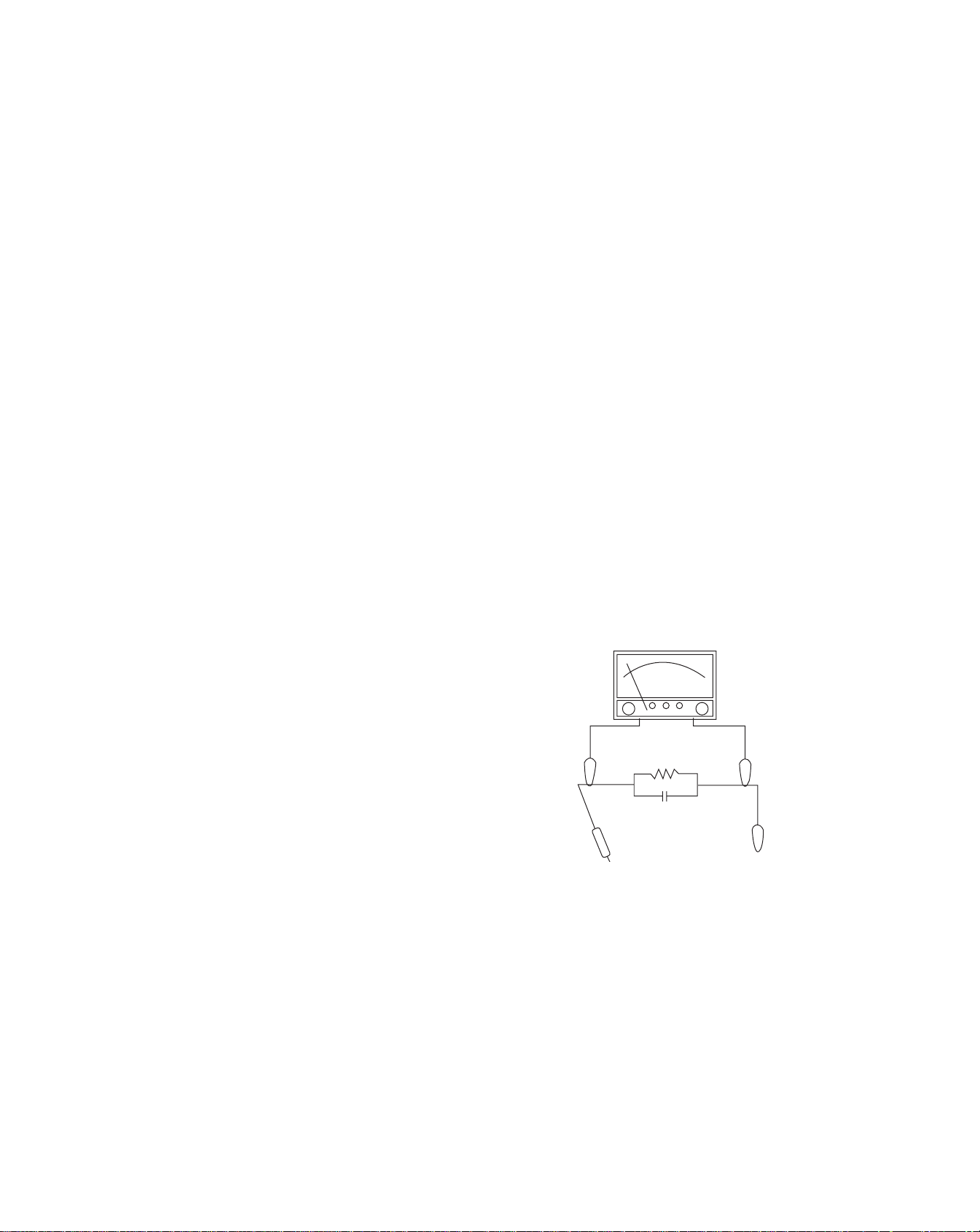
of measurement should be used. Using tw o clip leads, connect a 1500
ohm, 10 watt resistor paralleled by a 0.15 MF capacitor in series with
a known earth ground, such as a water pipe or conduit and the metal
part to be checked. Use a VTVM or VOM with 1000 ohms per volt, or
higher sensitivity to measure this AC voltage drop across the resistor .
Any reading of 0.61 volt RMS or more is excessive and indicates a
potential shock hazard which must be corrected before returning the
receiver to the owner .
Components shown in the shaded areas on the schematic diagram
or identified by the safety mark in the replacement parts list should
be replaced only with exact Factory recommended replacement parts.
The use of unauthorized substitute parts may create shock, fire,
X-radiation or other hazard.
To deter mine the presence of high voltage, use an accurate high
impedance HV meter connected between second anode lead and
the CRT dag grounding device. When servicing the High Voltage
System remove static charge from it by connecting 10K ohm resistor
in series with an insulated wire (such as a test probe) between picture
tube dag and 2nd anode lead (AC line cord disconnected from AC
supply).
The picture tube used in this receiver employs integral implosion
protection. Replace with tube of the same type number f or continued
safety. Do not lift picture tube by the neck. Handle the picture tube
only when wearing shatter-proof goggles and after discharging the
high voltage completely. Keep others without shatter-proof goggles
away .
When removing springs or spring mounting parts from tuner, tuner
cluster or chassis, shatter-proof goggles must be worn. Keep others
without shatter-proof goggles away.
SAFETY INSPECTION
Before returning the receiver to the user, perform the following safety
checks:
AC
VOLTMETER
1500 OHMS
0.15 µF
TEST
PROBE
TO EXPOSED
METAL PARTS
TO KNOWN
EARTH GROUND
X-RAY PROTECTOR CIRCUIT CHECK
PERFORM WHENEVER HIGH VOLTAGE CIRCUITRY OR POWER
SUPPLY CIRCUITRY IS SERVICED.
1. Plug the AC Line Cord (P1) into a AC 120V, 60Hz receptacle.
2. Turn the Power Switch (S101) on and wait for about 10 minutes.
3. Connect the antenna leads to the EXT. Antenna Terminal (TE1)
and select a broadcasting station.
4. Connect DC Digital Voltmeter to TP11 (positive lead) and TP4
(negative lead).
5. Apply DC 11V between TP11 and TP9 from external equipment.
6. If picture and sound do not disappear, check IC301, D552, D553,
D554, R554, R555, R556, R557, C555 and C556.
- 2 -
Page 4
te Control to select the
( ADJUSTMENT BY REMOTE CONTROL )
ADJUSTMENT MODE
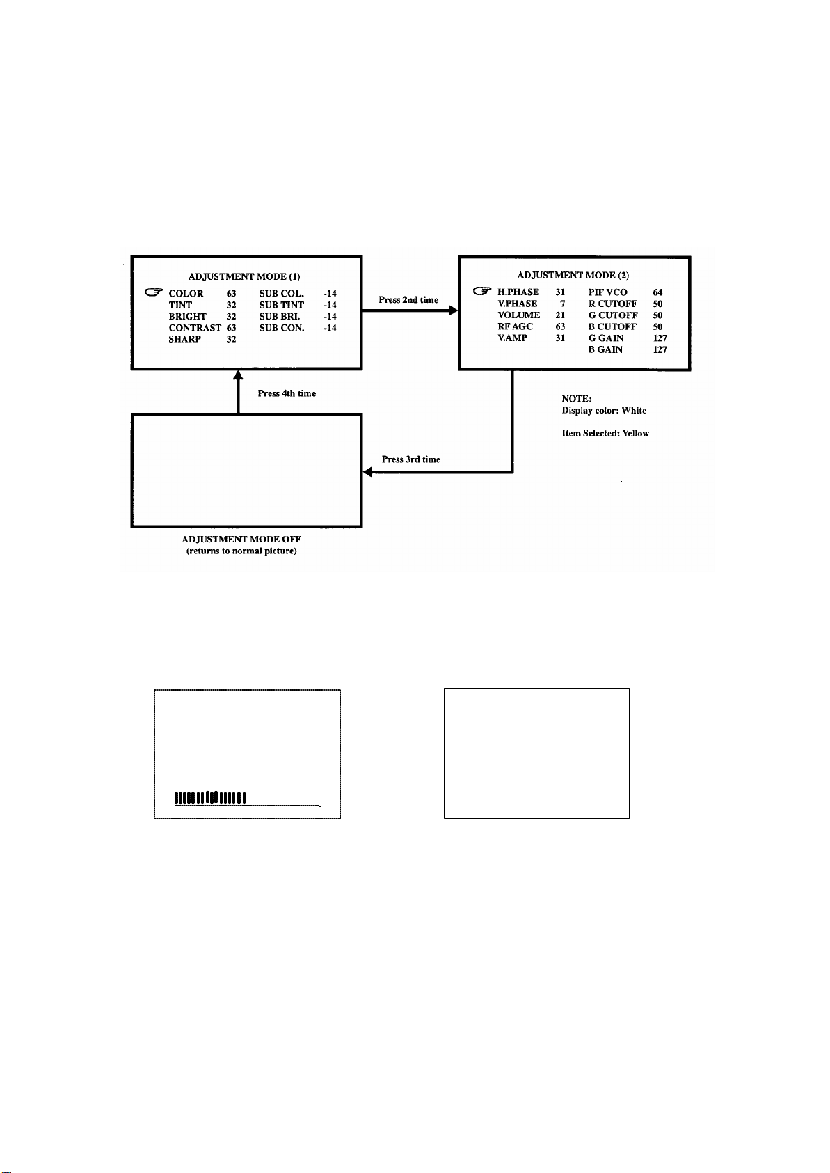
The following adjustment items can be performed from menus by Remote Control as shown
below :
NOTE: The button combination and position on the Remo
adjustment items is given on page 4.
1. Press the SHIFT + ADJ. MODE buttons on the Remote Control simultaneously to bring up
the adjustment mode menu screens shown below.
2. From the menu screen, press the + or - button on the Remote Control to select the item to
be adjusted.
3. Press the MENU button on the Remote Control to enter adjustment mode for the item
selected, and the display shown below appears :
OR
COLOR 32
RED CUTOFF 127
Example:
4. Use the + or - button on the Remote Control to adjust the data for the item selected.
5. When adjustment has been completed, press the SHIFT + ADJ. MODE buttons on the
Remote Control simultaneously to return to the main menu.
- 3 -
Page 5
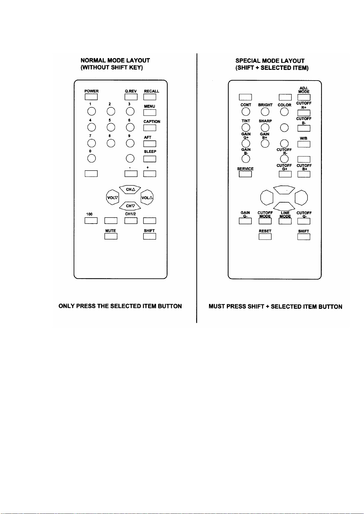
REMOTE CONTROL LAYOUT
VIDEO
VIDEO
- 4 -
Page 6

IC, TRANSISTOR AND CRT COMPLEMENT
INTEGRATED CIRCUITS
IC101 TA87C-B2 Microcomputer
IC102 M24CO2B EEPROM
IC301 TA1268N IF/Video/Chroma/Deflection
IC311 NJ7809FA Voltage Regulator
IC501 AN5512 Vertical Deflection Output
IC601 STR30130 AVR
IC671 NJ7805LD Voltage Regulator and Reset
TRANSISTORS
Q101 DTC143ZS Vertical Synchronizing
Q102 2SC945(P) Horizontal Synchronizing
Q173 2SC945(P) SD Signal Buffer
Q301 2SC945(P) SIF Signal Buffer
Q302 2SA733(P) Video Buffer Amplifier
Q303 2SC945(P) Video Out
Q351 DTC143ZS Service Mode Switching
Q451 2SC1573A(R) Red Color Driver
Q452 2SC1573A(R) Blue Color Driver
Q453 2SC1573A(R) Green Color Driver
Q551 2SC1473A(R) Horizontal Driver
Q552 2SD1877 Horizontal Driver
Q601 2SC945(P) Power On/Off Relay Driver
Q801 2SC945(P) Audio Amplifier
Q802 2SA950(0) Audio Amplifier
Q803 2SC2120(0) Audio Amplifier
PICTURE TUBE
V451 51GGD95X CRT (SUFFIX A) V451 A48LRH93X(W) CRT (SUFFIX C)
V451 510UEB22(DY) CRT (SUFFIX B) V451 A48LS D095X CRT (SUFFIX D)
V451 A48LGS30X CRT (SUFFIX E)
CHASSIS REMOVAL
1. Remove 4 screws (177) from Cabinet Back (AB) and remove Cabinet Back from rear.
2. Discharge anode lead at CRT chassis ground through a 10kohm resistor.
3. Disconnect anode lead from CRT.
4. Disconnect CRT Socket P.C. board (PCB -2) from CRT(V451).
5. Disconnect 3 connectors (CN501 (DY501), CN601 (L601) and LCN801) from Main P.C.
board (PCB -1).
6. When replacing chassis, reverse the above procedure making certain that all leads are
fastened in their original places.
CRT REMOVAL
CAUTION: Wear shatterproof goggles and exercise proper handling precautions when working
around high vacuum picture tubes.
1. Remove chassis per instructions under CHASSIS REMOVAL.
2. Remove Convergence Magnet Assembly (MG451) from neck of CRT.
3. Remove Deflection Yoke (DY501) from neck of CRT
4. Remove 3 wedges (142) from CRT
5. Remove Degaussing Coil (L601) from CRT
6. Remove braid wire (331) and spring (158) from CRT
7. Lay cabinet face down on some protective material.
8. Remove 4 CRT mounting screws (156).
9. Remove CRT from Cabinet Front (AA).
10. To install new CRT, reverse above procedure.
11. Perform purity and convergence adjustments.
- 5 -
Page 7
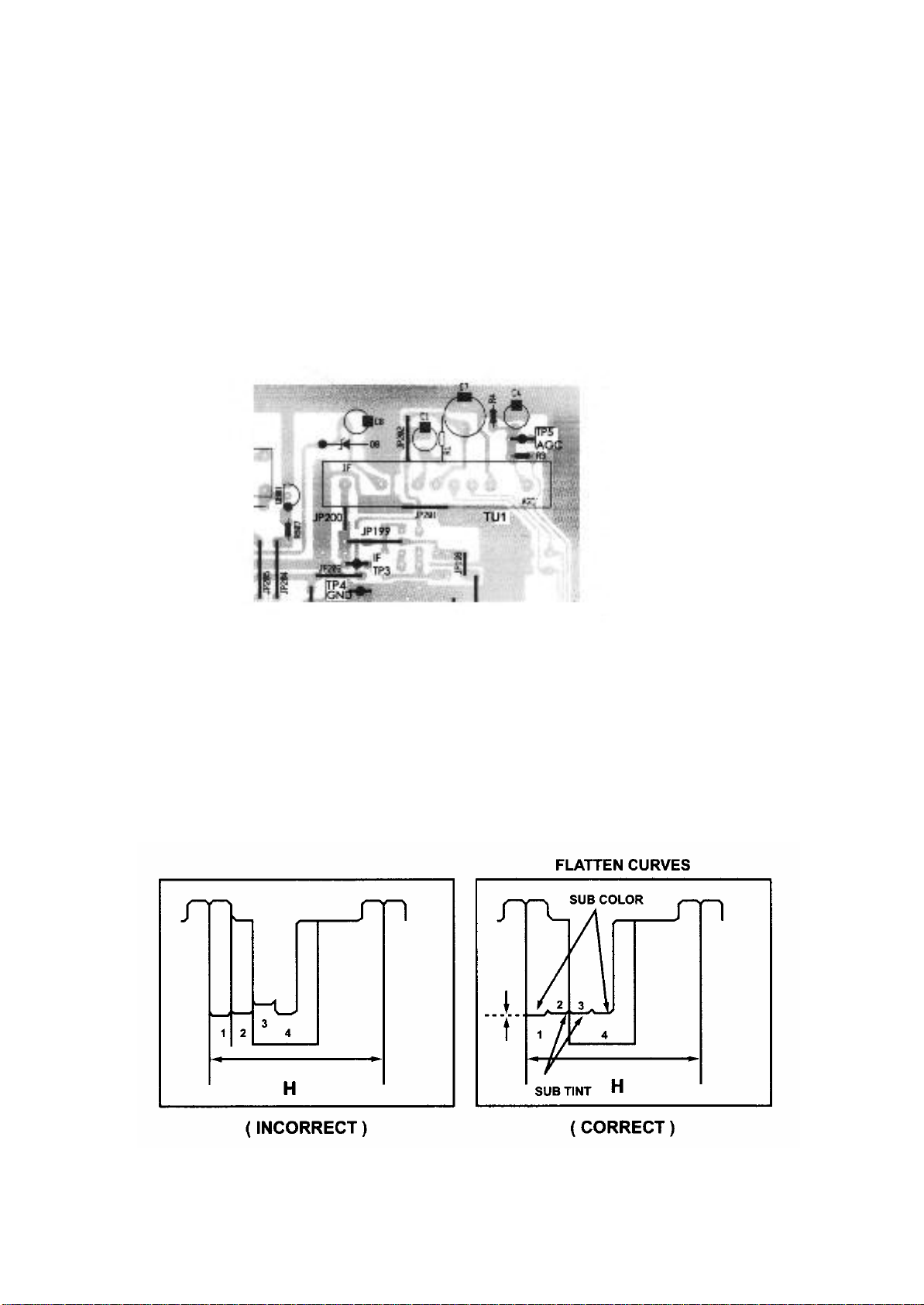
INSTALLATION AND SERVICE INSTRUCTION
CAUTION: Use an isolation transformer when performing any service on this chassis.
SHUTDOWN CIRCUIT: When the high voltage rises, there are simultaneous voltage increase
developed at terminal 6 of the Horizontal Output Transformer ( T671 ) and applied to pin 29 of IC301. If
excessive high voltage is produced, the increased voltage developed exceeds the rating of zener diode
D552 causing the Horizontal Oscillator to stop functioning and the high voltage system to shut down.
AFT ( AUTOMATIC FINE TUNING ) ADJUSTMENT
1. Remove JP200. (See Figure 1 for positioning)
2. Connect positive wire of TV signal Generator (NTSC signal, 45.75MHz, 80dBu ) to JP199 and
negative wire of TV Signal Generator to TP4.
3. Connect wire (+) of DC Digital Voltmeter to TP6 and wire (-) to TP4.
4. Adjust T202 so that the DC Digital Voltmeter reading is 2. 5V ± 0.2V.
5. Re insert JP200 and put solder.
FIG. 1
SUB TINT ADJUSTMENT
1. Connect TV Test Pattern Generator (NTSC signal, Color Bar signal, 70dB u , channel 6) to EXT.
Antenna Terminal (TE1) through TV Channel Signal Generator.
2. Connect positive lead of Oscilloscope to TP14 and negat ive lead to TP10.
3. Connect EXT. trigger of Oscilloscope to R463.
4. Set Tint control to center position. (by Remote Control).
( NOTE: For steps 5, 6 and 7 below, refer to page 3 for Adjustment By Remote Control Method).
5. Go to Adjustment Mode (1) by remote control.
6. Select SUB TINT from Adjustment Mode (1) menu screen.
7. Adjust SUB TINT level (by using + or - button on remote control) so that waveform is the same as
shown in Figure 2.
FIG. 2
- 6 -
Page 8
SOUND IF ADJUSTMENT
1. Connect TV Test Pattern Generator (NTSC signal, 70dB u, channel 2) to EXT. Antenna Terminal (TE1) through
TV Channel Signal Generator. (Standard modulation is 400Hz at 25kHz deviation for sound signal.
2. Connect positive lead of DC Digital Voltmeter to TP7 and negative lead to TP4.
3. Adjust T203 so that the DC Digital Voltmeter reading is 4.0V.
COLOR PURITY ADJUSTMENT
For best results, it is recommended that the purity adjustment be made in the final receiver location. If the receiver
will be moved, perform this adjustment with it facing East.
The receiver must have been operating 15 minutes prior to this procedure and the face plate of the CRT must be at
room temperature. The following procedure is recommended while using a Dot/Bar Generator.
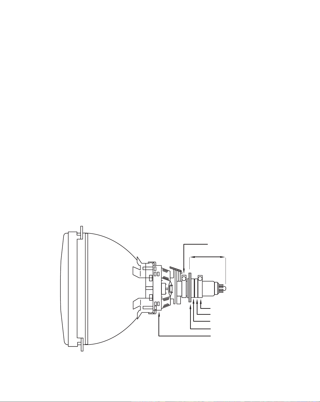
1. Check correct location of all neck components. (Refer to Fig. 3)
2. Rough-in the static convergence at the center of the CRT, as explained in the static convergence procedure.
3. Set the Contrast control to minimum position and Brightness control as far maximum as possible without
causing the picture to “bloom”.
4. Apply green raster signal from Dot/Bar Generator to receiver.
5. Loosen the deflection yoke clamp screw and pull the deflection yoke toward the rear of the CRT.
6. Begin the following adjustment with the tabs on the round purity magnet rings set together. Slowly separate
the two tabs while at the same time rotating them to adjust for a uniform green vertical band at the center of
the CRT screen.
7. Carefully slide the deflection yoke forward to achieve green purity (Uniform green screen).
(NOTE: Center purity is obtained by adjusting the tabs on the round purity magnet rings. Outer edge purity is
obtained by sliding the deflection yoke forward.)
8. Check for red and blue field purity by applying red and blue raster signal alternately from Dot/Bar Generator to
receiver. Repeat steps 2 through 7, if required.
9. Tighten deflection yoke clamp screw.
10. Perform BLACK AND WHITE ADJUSTMENT procedure.
(CW : clockwise, CCW : counterclockwise)
Fig. 3
- 7 -
CLAMP SCREW
65.0 mm
(2.56 inches)
CLAMP SCREW
6 POLE MAGNETS
4 POLE MAGNETS
PURITY MAGNETS
DEFLECTION YOKE
Page 9
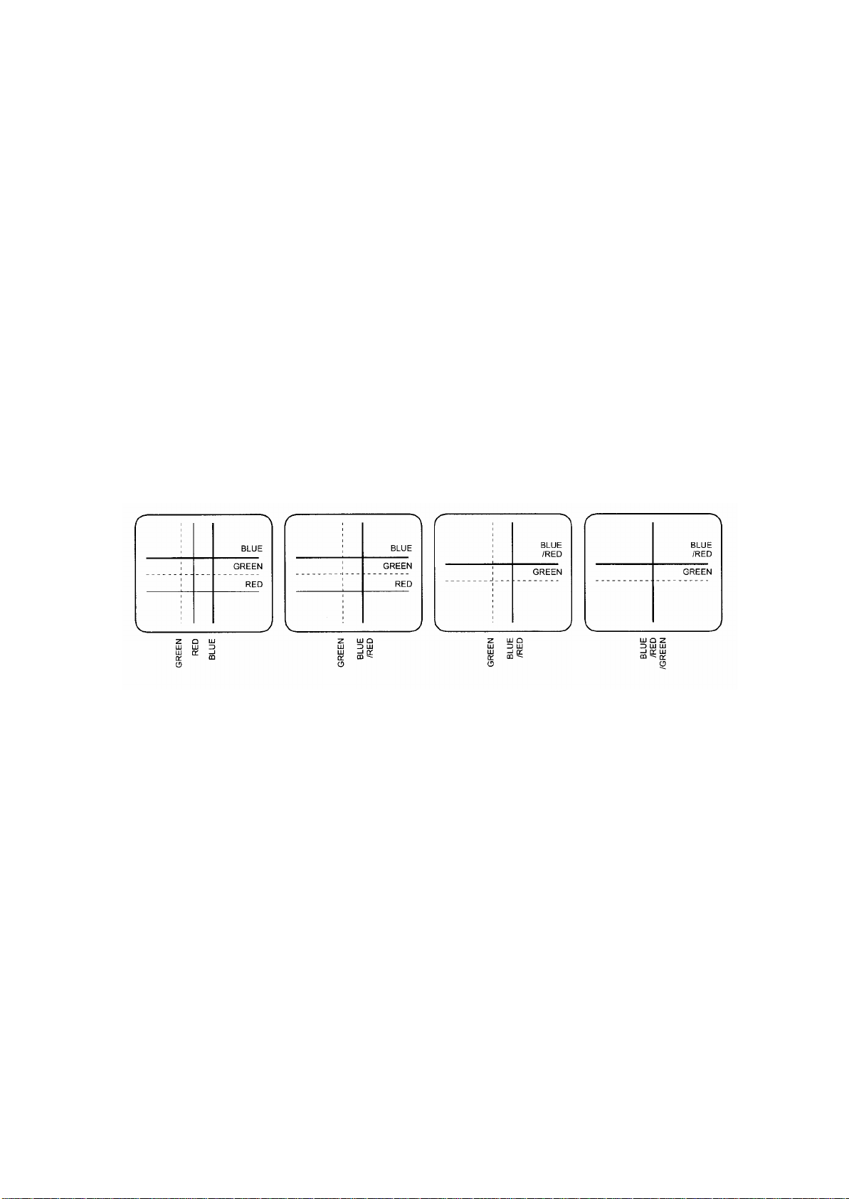
STATIC CONVERGENCE ADJUSTMENT ( Refer to Figure 3 and 4 )
IMPORTANT: Before proceeding, make sure the location of the convergence magnet assembly on the
neck of the CRT is as shown in Figure 3. The rear edge of this assembly must be positioned 65 mm
from the tip of the CRT base. If not properly positioned, convergence adjustment may be difficult, if not
impossible.
1. Apply dot or crosshatch pattern from Dot/Bar Generator to receiver. Reduce setting of Brightness
and/or Contrast controls to eliminate any blooming in pattern.
2. Observe the blue and red pattern appearing on the CRT screen. Locate the 4 pole magnet rings
and separate their adjusting tabs approximately the width of one tab.
3. Now rotate this pair of magnet rings as a unit without re-adjusting the spacing between the tabs.
This will minimize the separation between the blue and red dots (lines).
4. If the blue and red dots are not completely converged at this point, readjust the spacing between the
two tabs to complete convergence of the blue and red dots (lines), thus producing magenta dots
(lines).
5. If necessary, repeat step 2, 3 and 4 until proper convergence is achieved.
6. Observe the magenta (B/R) and green pattern now appearing on the CRT screen.
7. Locate the 6 pole magnet rings and separate their adjusting tabs approximately the width of one tab.
8. Rotate this pair of magnet rings as a unit without re-adjusting the spacing between the tabs. This
will minimize the separation between the magenta (B/R) and green dots ( lines).
9. If the magenta and green dots (lines) are not completely converged at these points, readjust the
spacing between the two tabs to complete convergence of the magenta and green dots (lines).
10. If necessary, repeat step 7, 8 and 9 until proper convergence is obtained.
To prevent accidental mis-adjustment of the magnets, apply a stripe of paint across all six rings and
onto the neck of the CRT.
FIG. 4
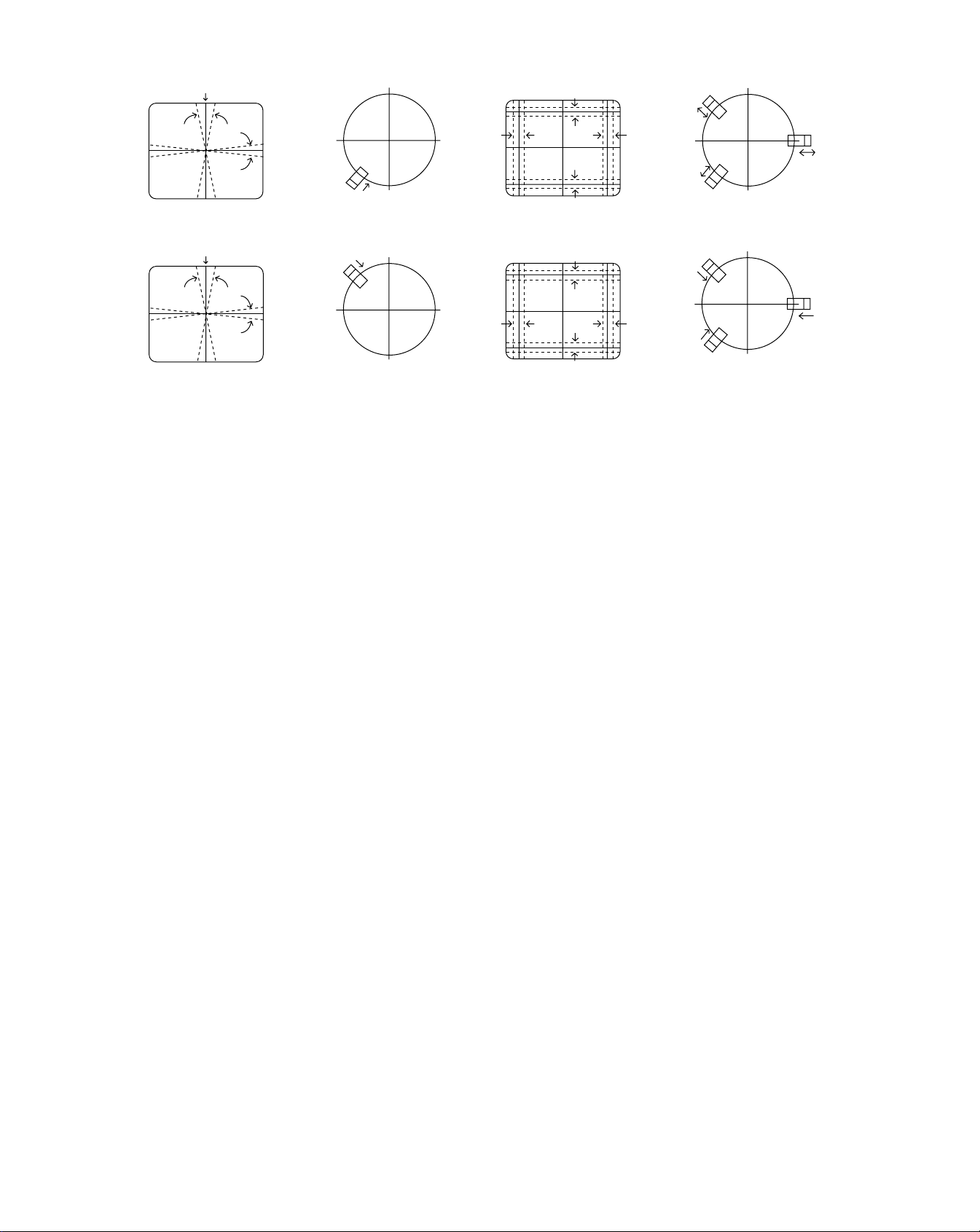
DYNAMIC CONVERGENCE ADJUSTMENT ( Refer to Figure 5)
Dynamic convergence (convergence of the three edges of the CRT screen) is accomplished by proper
insertion and positioning of three rubber wedges between the edges of the deflection yoke and funnel of
the CRT. This is accomplished in the following manner.
1. Turn the receiver ON and allow it to warm up for 15 minutes.
2. Apply crosshatch pattern from Dot/Bar Generator to receiver. Observe spacing between lines around
edges of CRT screen.
3. For the misconvergence shown in Figure 5 ( A ), tilt the deflection yoke down and insert wedge A
between deflection yoke and CRT.
4. For the misconvergence shown in Figure 5 ( B ), tilt the deflection yoke up and insert wedge B
between deflection yoke and CRT.
5. For the misconvergence shown in Figure 5 ( C), tilt left side of the deflection yoke and slightly insert
wedge C between deflection yoke and CRT. Then, deeply insert wedges A and B between deflection
yoke and CRT.
6. For the misconvergence shown in Figure 5 ( D ), tilt right side of the deflection yoke and deeply insert
wedge C between deflection yoke and CRT. Then, slightly insert and/or extract wedges A and B
between deflection yoke and CRT.
7. Alternately change spacing between and depth of insertion of the three wedges until proper dynamic
convergence is obtained.
8. Use a strong adhesive tape to firmly secure each of the three rubber wedges to the funnel of the
CRT.
- 8 -
Page 10
GREEN
(A)
(B)
(D)
RED BLUE
RED
GREEN
BLUE
WEDGE A
DEFLECTION YOKE REAR VIEW
RED
GREEN
BLUE
RED BLUE
GREEN
(C)
GREEN
BLUE RED
BLUE
GREEN
RED
WEDGE B
WEDGE C
WEDGE A
DEFLECTION YOKE REAR VIEW
GREEN
BLUE RED
BLUE
GREEN
RED
WEDGE B
DEFLECTION YOKE REAR VIEW
BLUE
GREEN
RED
BLUE RED
GREEN
GREEN
RED BLUE
RED
GREEN
BLUE
WEDGE B
WEDGE C
WEDGE A
DEFLECTION YOKE REAR VIEW
Fig. 5
FOCUS ADJUSTMENT
Adjust focus control, located on the Horizontal Output Transformer (T671), for maximum ov er all definition and fine
picture detail with Brightness and Contrast controls set at normal viewing levels.
BLACK AND WHITE ADJUSTMENT (CUTOFF / WHITE BALANCE)
The purpose of this procedure is to adjust the bias applied to the color picture tube for reproducing a quality
monochrome picture at all brightness levels and also to achie ve maximum usable brightness. Confirm that proper
purity and AGC adjustments have been completed before starting this adjustment.
1. Connect the TV test pattern generator (Monoscope pattern) to the EXT. antenna terminal via TV VHF/UHF
signal generator (NTSC signal, 70dB u).
2. Select Cutoff Mode by remote control, (refer to page 4 for remote control key combination and position) and
CUT OFF will be displayed on top-right screen for about 3 seconds. At the same time the data readings for
Cutoff and Gain in Adjustment Mode (2) will become as follows:
R CUTOFF: 50, G CUTOFF: 50, B CUTOFF: 50, G GAIN: 127, B GAIN: 127
3. Select Service Mode by remote control, (refer to page 4 for remote control key combination and position) and
TV screen becomes horizontal line.
4. Turn the Screen control (located under the flyback transformer) clockwise until any blue, green or red color
line appears.
5. Check the color of the line which appeared first, then turn the Screen control (located under the flyback
transformer) fully counterclockwise.
6. Adjust the cutoff level of the color which appeared first by remote control, (refer to page 4 for remote control
key combination and position) so that voltage between TP16 and TP15 (blue), TP14 (green) or TP13 (red) is
20 ± 1V.
7. Turn the Screen control (located under the flyback transformer) clockwise so that the bright color line can just
be seen.
8. Adjust cutoff levels other than the above by remote control, (refer to page 4 for remote control key combination
and position) so that the line color is white.
9. Press again Service Mode key by remote control, (refer to page 4 for remote control key combination and
position) to return to TV position. Monoscope pattern will appear on TV screen.
10. Adjust the contrast and brightness controls to make the picture dim. Adjust the Green and Blue Cutoff levels
by remote control, (refer to page 4 for remote control key combination and position) so that the picture is white.
11. Adjust the contrast and brightness controls to make the picture bright. Adjust the Green and Blue Gain levels
by remote control, (refer to page 4 for remote control key combination and position) so that the picture is white.
12. Repeat steps 10 and 11 so that the picture is white in both dim and bright conditions.
- 9 -
Page 11
HORIZONTAL PHASE ADJUSTMENT
2.
'0' (using + or - button on remote control).
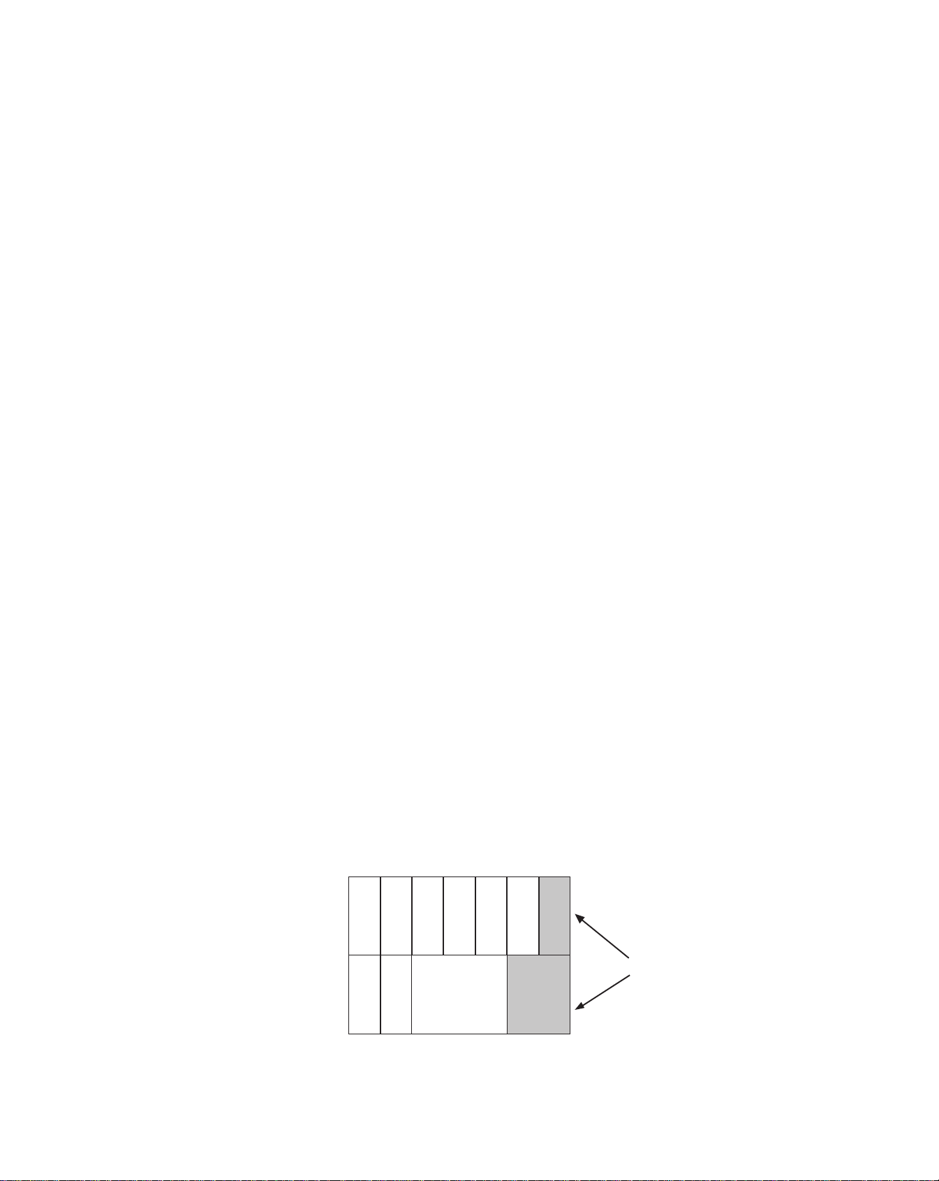
Adjust SUB BRIGHT level (by using + or - button on remote control) to obtain a dim pattern. (Refer to Fig.6)
1. Connect TV Test pattern Generator (NTSC signal 70dB u, Monoscope Pattern) to Antenna T erminal
(TE) through TV Channel Generator.
(NOTE: For steps 2, 3 and 4 below, refer to page 3 for Adjustment By Remote Control Method).
2. Go to Adjustment Mode (2) by remote control.
3. Select H. PHASE from Adjustment Mode (2) menu screen.
4. Adjust H. PHASE level (by using + or - button on remote control) so that horizontal reading of test pattern
becomes the same value.
VERTICAL PHASE ADJUSTMENT
1. Connect TV Test pattern Generator (NTSC signal 70dB u, Monoscope Pattern) to Antenna Terminal
(TE) through TV Channel Generator.
(NOTE: For steps 2, 3 and 4 below, refer to page 3 for Adjustment By Remote Control Method).
2. Go to Adjustment Mode (2) by remote control.
3. Select V. PHASE from Adjustment Mode (2) menu screen.
4. Adjust V. PHASE level (by using + or - button on remote control) so that vertical reading of test pattern
becomes the same value.
VERTICAL AMPLITUDE ADJUSTMENT
1. Connect TV Test pattern Generator (NTSC signal 70dB u, Monoscope Pattern) to Antenna Terminal
(TE) through TV Channel Generator.
(NOTE: For steps 2, 3 and 4 below, refer to page 3 for Adjustment By Remote Control Method).
2. Go to Adjustment Mode (2) by remote control.
3. Select V. AMP from Adjustment Mode (2) menu screen.
4. Adjust V. AMP lev el (b y using + or - b utton on remote control) so that picture fills the picture opening from top
to bottom and is proportionate to the width.
RF AGC ADJUSTMENT
1. Connect TV Channel Signal Generator to Antenna Terminal (TE).
2. Connect positive lead of DC Digital Voltmeter to TP5 and negative lead of DC Digital Voltmeter to TP4.
3. Adjust level of TV Channel signal Generator so that the output level is 57dB u. (Monoscope Pattern)
(NOTE: For steps 4, 5 and 6 below, refer to page 3 for Adjustment By Remote Control Method).
4. Go to Adjustment Mode (2) by remote control.
5. Select RF AGC from Adjustment Mode (2) menu screen.
6. Adjust RF AGC level (by using + or - button on remote control) so that the DC Digital Voltmeter reading is 6.0V
± 0.2V.
SUB BRIGHTNESS ADJUSTMENT
1. Connect TV Test Pattern Generator (NTSC signal, Color Bar Signal, 70dB u) to EXT. Antenna Terminal through
TV Channel Signal Generator.
(NOTE: For steps 3, 4 and 5 below, refer to page 3 for Adjustment By Remote Control Method).
Go to Adjustment Mode (1) by remote control.
3. Set the COLOR and CONTRAST of the TV set to minimum and the SUB CONTRAST and SUB BRIGHT to
4.
DIM LIGHT
Fig. 6
- 10 -
Page 12
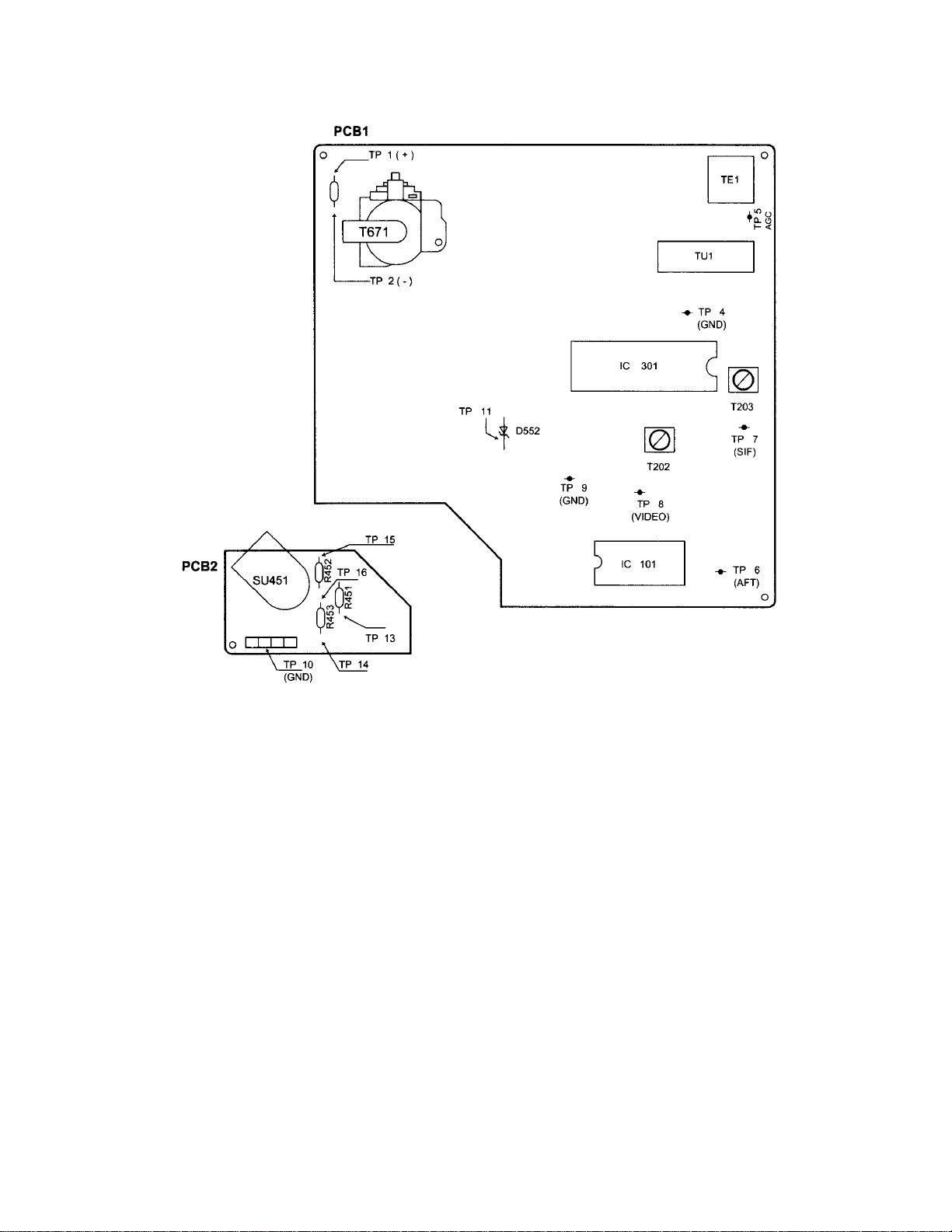
TEST POINT
- 11 -
Page 13
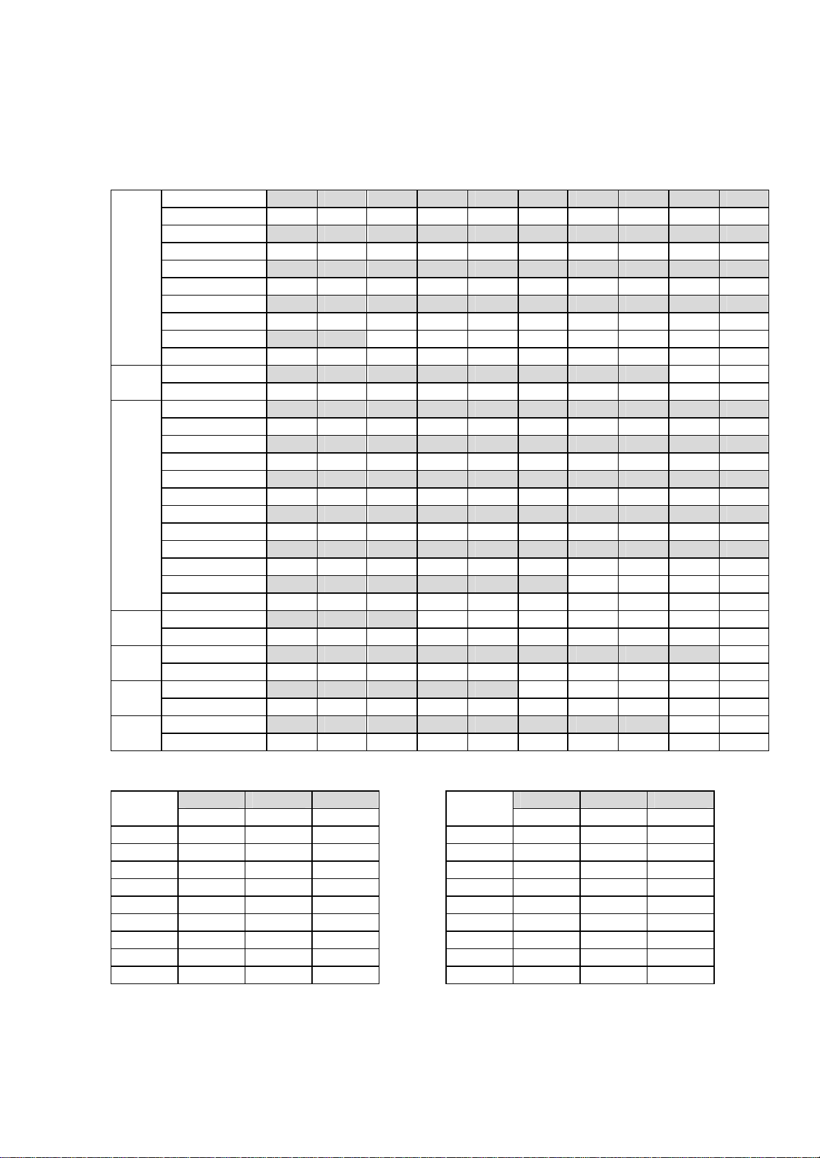
VOLTAGE CHART ( all in volts )
OPERATION CONDITION : TINT, BRIGHT and COLOR CONTROL……….. CENTER
CONTRAST ………………………………………. MAXIMUM
COLOR BAR SIGNAL
IC101 TERMINAL No 1 2 3 4 5 6 7 8 9 10
Volt 0.0 0.0 0.0 0.0 5.0 5.0 5.0 0.0 0.0 1.0
TERMINAL No 11 12 13 14 15 16 17 18 19 20
Volt 0.0 0.0 5.0 5.0 5.0 2.9 0.0 0.0 1.0 1.0
TERMINAL No 21 22 23 24 25 26 27 28 29 30
Volt 4.9 0.0 0.0 0.0 0.0 3.8 4.3 4.8 4.9 0.0
TERMINAL No 31 32 33 34 35 36 37 38 39 40
Volt 2.1 2.3 5.0 0.0 5.0 4.5 3.0 2.0 0.0 0.7
TERMINAL No 41 42
Volt 0.7 5.0
IC102 TERMINAL No 1 2 3 4 5 6 7 8
Volt 0.0 0.0 0.0 0.0 1.9 3.0 0.0 5.0
IC301 TERMINAL No 1 2 3 4 5 6 7 8 9 10
Volt 0.0 3.9 2.3 3.4 4.4 0.0 2.0 1.2 9.1 5.8
TERMINAL No 11 12 13 14 15 16 17 18 19 20
Volt 6.5 4.9 0.0 0.0 4.8 4.8 4.8 3.2 2.3 2.1
TERMINAL No 21 22 23 24 25 26 27 28 29 30
Volt 2.2 0.7 4.7 4.8 6.5 9.1 3.0 1.9 2.8 1.2
TERMINAL No 31 32 33 34 35 36 37 38 39 40
Volt 0.7 1.2 7.7 6.3 0.0 2.9 3.2 3.0 1.6 5.2
TERMINAL No 41 42 43 44 45 46 47 48 49 50
Volt 3.0 5.0 5.0 2.0 1.8 9.1 4.0 9.1 8.1 8.1
TERMINAL No 51 52 53 54 55 56
Volt 0.0 0.0 2.8 4.0 2.8 0.0
IC311 TERMINAL No 1 2 3
Volt 16.0 0.0 9.0
IC501 TERMINAL No 1 2 3 4 5 6 7 8 9
Volt 0.0 11.4 0.0 23.0 12.6 0.0 -0.3 1.6 25.4
IC601 TERMINAL No 1 2 3 4 5
Volt 0.0 121.0 160.0 160.0 0.0
IC671 TERMINAL No 1 2 3 4 5 6 7 8
Volt 14.0 0.0 5.5 0.0 0.0 4.6 0.0 5.0
B E C B E C
Volt Volt Volt Volt Volt Volt
Q101 1.5 0.0 4.3 Q453 2.1 2.0 149
Q102 -0.8 0.0 3.8 Q551 0.3 0.0 84.4
Q173 -0.1 0.0 4.5 Q552 -0.2 0.0 Q301 4.0 3.4 9.1 Q601 0.7 0.0 0.2
Q302 1.5 2.1 0.0 Q801 0.7 0.0 7.1
Q303 1.7 1.1 9.1 Q802 7.1 7.8 0.0
Q351 0.0 0.0 9.1 Q803 8.4 7.8 16.0
Q451 2.3 2.2 139
Q452 2.2 3.2 145
- 12 -
Page 14
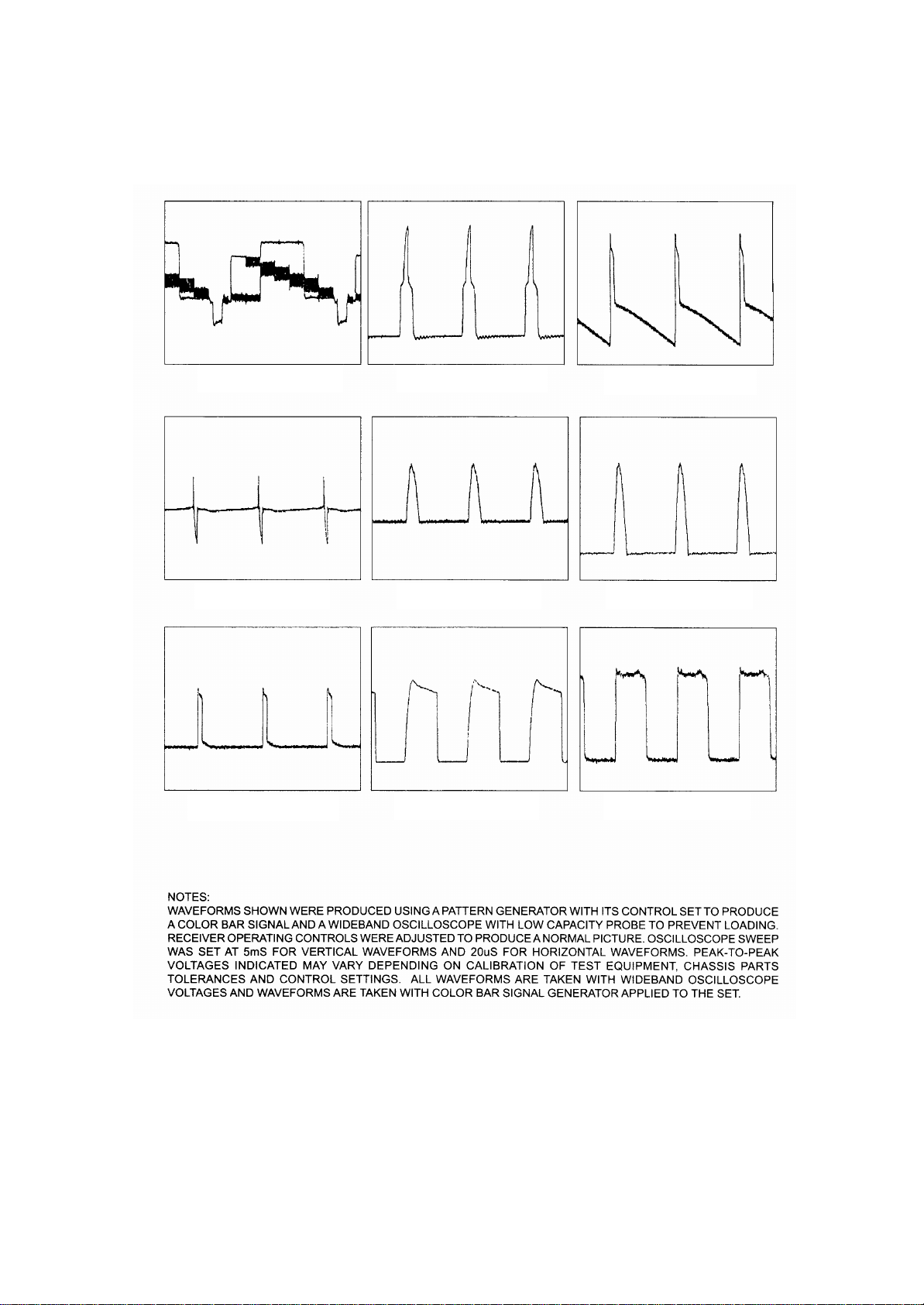
WF-7 25.8Vp
-
p(V) WF-8 202Vp
-
p(H) WF-9 0.75Vp
-
p(H)
CHASSIS WAVEFORM
WF-1 1.0Vp-p(H) WF-2 9.7Vp-p(H)
WF-4 1.7Vp-p(V)
WF-5 27.4Vp-p(H)
WF-3 47.2Vp-p(V)
WF-6 24.4Vp-p(H)
- 13 -
Page 15
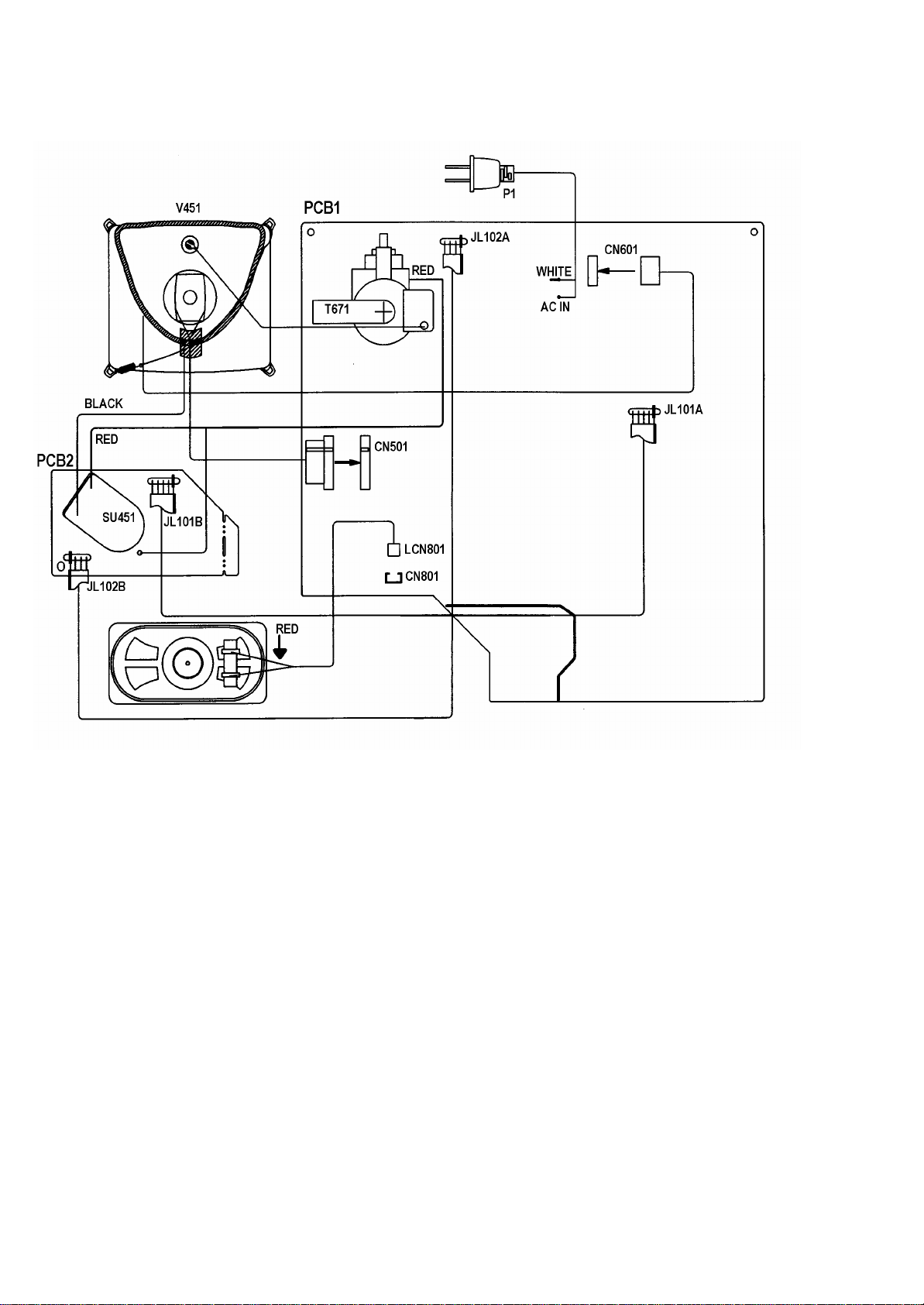
WIRING DIAGRAM
- 14 -
Page 16
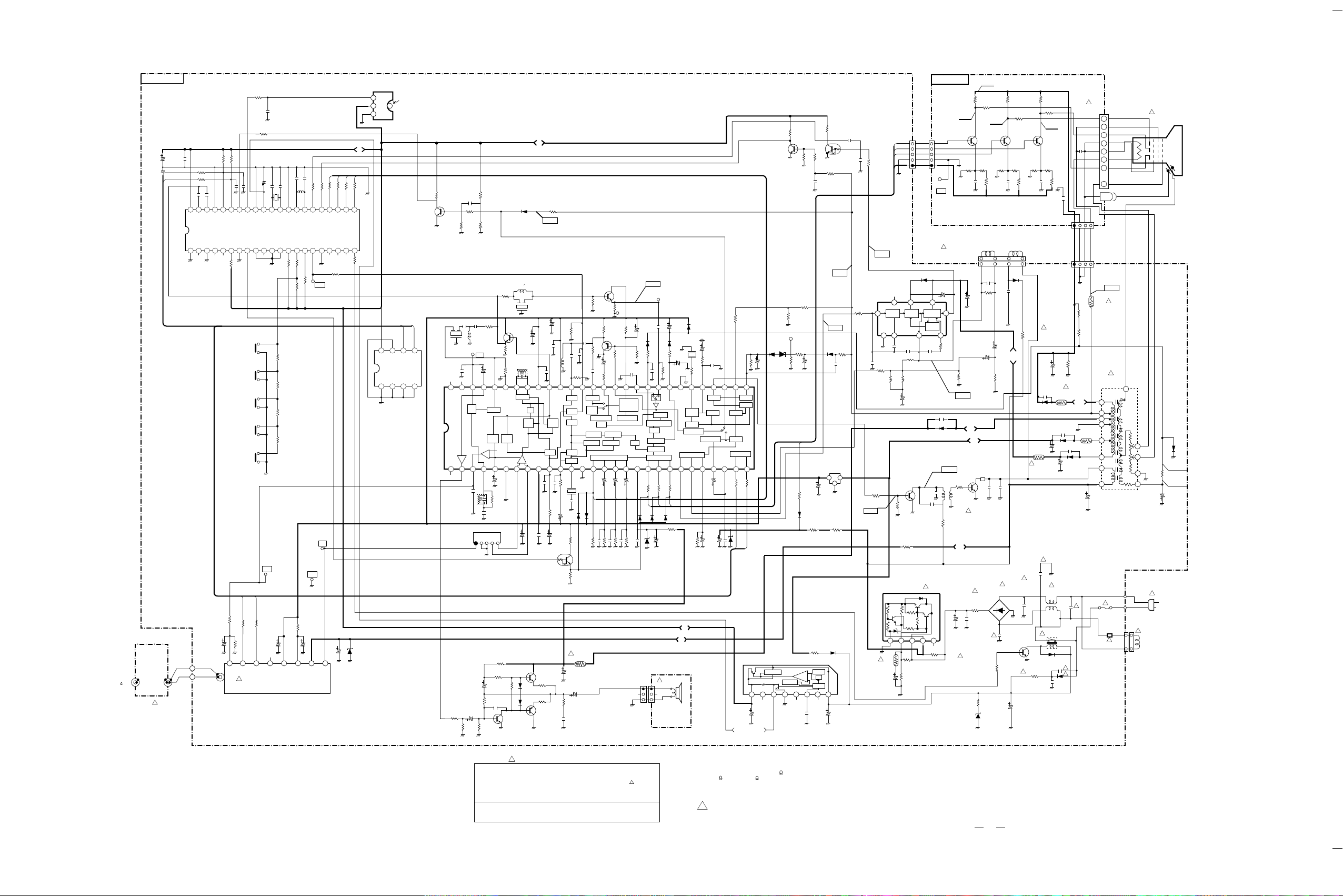
SCHEMATIC DIAGRAM
UHV/VHF
75
PCB1 MAIN 4551-2011601D
ZF
C108
C107
100 /10V
!
TE 1
0.022
42 41 40 39 38 36 3537
IC101
U-COM
TMPA8700CPN
1k
R105
4.7k
R101
R103 100
R104 100
C101 0.1
C102 0.1
VCC
GND
VIDEO INPUT
VIDEO INPUT
GND
NC
V-SYS
NC
1 2 345 76
R3
10k
C4
4.7 /50V
R142
1 k
1/4W
C180
100p B
R146 1 k
C104
34 3233
GND
REMOTE
SERVICE
LANGUAGE
S101
POWER
S102
CH-UP
S103
CH-DOWN
S104
VOL-UP
S105
VOL-DOWN
R151
1k 1/4W
C105
27p CH
27p CH
C103
4.7/50V
X101 8MHz
30311229 2728 2526 24 2223
XIN
XOUT
RESET
TV/VIDEONCMAIN/SAP
VCHIP SEL
13 14 161517 18 19 2120
22k
R112
3.3k
R131
3.3k
R132
5.6k
R133
12k
R134
TP5
AGC
R152
1k 1/4W
C7
330 /16V
TEST
4.7k
R102
C111
C112
680pB
680pB
SCL
SDA
H. SYNC
ST/MONO
V-BLOCK
POWER IN
891110
22k
R106
R4 180k
AGC
SCL SDA BM BP BT IF
TU1
!
VHF/UHF/CATV TUNER
C106
1k
R114
10k
R113
R1
220 1/4W
30p CH
L101
OSC1
KEY IN
47uH
C109
8.2p CH
R120 1k
R119 1k 1/4W
OSC2
VD-OSD
AFC
MENU COLOR
22k
R110
TP6
AFT
TP3
IF
TP4
GND
C1
10 /50V
BLK
R121
R122
5.6k 1/4W
BLK
HD-OSD
ADJ MODE 3
NC
R116
1k
B
G
R123
5.6k 1/4W
5.6k 1/4W
B
OSD CONT 1
C8
22 /50V
5V
R
R124
5.6k 1/4W
R
G
OSD CONT 2
POWER
R105
D8
HZT33
1k
VOUT
RX101
VCC
REMOTE
SENSOR
GND
8 7 6 5
WC
VCC
IC102
M24C02
E0E1E2
1 2 3 4
PCB2 CRT
R128
2.2k
2SC945 (P)
D553
1SS133
/50V
D552
RD6R8ES2
NJ7805LD
PROTECT
Q102
2.2k
R336
IC671
F. BACK
G CD
R555
1/6W
TP11
X-RAY
15k
R614
C681
R129
C129
100p
R328
2.2k
R556
5.6k
C556
680 1/4W
D607
1SS133
3.9k 2W MTL
ERROR
0.1
MYL
5V
10K
1/4w
R176
SCL
SDA
VSS
C177
18k
1/4W
R179
270p
Q173
R177
2SC945 (P)
33k
R180
R178
68k
56k
1/6W
C217
47p
CH
R218
1k
C218
47p
CH
2
L203
22uH
TP7
SIF
C212
4.7
50V
FM
DET
LOCK
IC301
TA1268N
1 3
CF201
4.5MHz
C213
4700p
BPF
B
1 2 3 4 5 6 137 8 9 1110 12 14 15
T203
C221
0.01
ZF
C206
1000p
SF201
45.75MHz
C802
47 /16V
10k
R804
R801
C801
470
4.7 /50V
1k
10k
R802
R803
2SC945 (P)
LIMIT
DET
B
2200p
R806
C803
Q801
AGC
R212
R805
150
R306
330
R220
RF
470
SIF
GND
LOCK
GND
C211
10k
1k
DET
PIF
D306
R181
1SS133
33k
WF-2
L301
15 uH
1 3
CF301
C318
4.5MHz
47
TRAP
2
Q301
2SC945 (P)
1.8k
R301
4.7 /50V
C209
47
/16V
D801
1SS133
150
R807
D802
1SS133
/16V
C232
47
/16V
C317
0.01
C220
2200p B
390
R123
C208
0.47
/50V
DTC143ZS
R808
R809
2.2 1/6W
DET
1
Q351
C231
0.01 ZF
VCC
C320
0.022 ZF
R350
C806
L361
5.6uH
BPF
AFT
ACC
APCSW
VCXO
R322
C319
C322
0.47
/50V
470
1000 /16V
220 /16V
R810
C805
C361
R362
39K
3.58MHz
3.3k
10p CH
!
10 1/2W
C804
2.2
0.1
T202
VCO
SIF
VCC
VCO
90
Q
DET
PIF
VCC GND 3.3V H.VCC
C210
0.01
ZF
Q803
2SC2120 (O)
1 1/6W
Q802
2SA950 (O)
56k
R214
C362
100p
1000p MYL
44 4243 4041 39 37 36 35 34 33 32 31 30 29385556 54 53 52 5051 49 4748 4546
X301
D312 1SS133
220
R351
R812
Q303
2SC945 (P)
330
R307
R305
R361
C214
0.01 ZF
C303
CLAMP
3.58
TRAP
DC REST
Y-DL
COLOR
KILL
ANALOG RGB
C341
D308 1S2473
10k
R344
C346
R343
GND
TP9
1k
R308
3.3k
R330
Q302
220k 1/6W
2SA733 (P)
1k
R303
1.8k 1/4W
C331
C391
1/50V
0.01
75k
0.1 MYL
R391
BLACK
STRETING
WPS
SMOOTH
DEMO
TINT
16 17 18 19 2120
C342
C343
0.1 /50V
0.1 /50V
0.1 /50V
B
R
G
820
820
R342
B
B
B
100p
100p
100p
C345
C344
CN801
R302
LPF
R341
C308
/50V
1.8k
820
C381
10
0.01ZF
WF-1
C306
0.1
MYL
D301
1S2473
CONTRAST
WPL
BRIGHT
MATRIX
CUTOFF
R319 220
R
D309
1SS133
D555
VIDEO
TP8
C315
2.2
/50V
X551
503KHz
D303
1S2473
R331
390k
R335
120k 1/6W
1/6W
C305
1 /50V
R340 1M
C304 0.01
SHARP
H-SEP.
V. RAMP
22 23 24 25 26 27 28
R320 220
R321 220
B
G
D311
D310
1SS133
1SS133
R381
820 1/2W
3.3V
C380
1/50V
5V
33V
!
LCN801
SP801
8 OHM
SPEAKER
32fH
VCO
HC/D
R518
D302
1SS133
R570
18k
1/6W
390
V-SEP.
C501
H. VCC
C562
1 /50V
R551
2.2k
1/4W
C551
0.01
ZF
H-OUT X-RAY
AFC1
AFC2
VC/D
BUS
C552
2.2 /50V
R192 1k
C554
100 /16V
C553
2.2 /50V
0.01 ZF
RESET OUTPUT
5.6k
R329
10
C555
47k
R554
H.RAMP
R191 1k
D559
RD9R1ES2
ROUT
VOUT
8 7 6 5 4 3 2 1
C682
2200
/6.3V
R136
10k
B
10
/50V
OUT IN
C664
100 /16V
R613
R615
47 1/4W
START
V
RESET
22k
R126
Q101
DTC143ZS
100k
R137
15k
WF-5
WF-4
D554
R557
1SS133
C130
100p
3 1
9V
2
IC311
NJ7809FA
VOLTAGE
REGULATOR
R612
3.9k 2W MTL
D606
1S2473
VIN
C678
100
/25V
C126
560p B
1000p B
1k
C127
R503
100
1/4W
C503
0.033
MYL
WF-9
270k
1/4W
R127
WF-7
IC501
AN5512
VERTICAL
DEFLECTION
OUTPUT
DRIVER
6
STAGE
C512
100p B
R501
1k
R558
330
1 2 3 4 5
!
R606
C608
JL101A
5P
R
G
B
9V
JL101
D501
1N4002E
3 4 9
OUTPUT
STAGE
C504
470p B
R507
56k
R510
5.6k
56k
1/6W
R519
C510
3.3
/50V
Q551
2SC1473A (R)
R559
330
R674
1.8k 1W MTL
IC601
STR30130
R604
12k 1W
47 1/4W
R605
22 /160V
330k 1/4W
JL101B
5P
R
G
B
9V
TP10
GND
4551-2011602D
!
DY501
DEFLECTION YOKE
C506
100/35V
FLYBACK
8
GENERATOR
PULSE
SHAPER
7251
C505
0.1
MYL
R504
D681
1F4-E
WF-8
C558
560p
/500V
T552
3 4
1
C557
680p
/500V
2.2k 5W CEM
!
C607
R603
270
15W
CEM
15k
6
R451
TP13
Q451
1573A (R)
RED
R457
1/6W
CN501
R508
33k
WF-3
C683
0.01/400V
R562
0.5
1/2W
Q552
2SD1877
R561
130V
470 /200V
!
TP16
MTL
C511
FB551
!
2.7
5W
MTL
C606
R454
3.3k 1/2W
Q452
1573A (R)
BLUE
R458
1.2k
1/4W
C451
680p B
VERTICAL
C507
0.047
MYL
R505
390
100 /35V
1/4W
C509
2.2
/50V
L.L
C561
0.01 /250V
R607
4.7k
R611
680
1/2W
D605
RD12ES2
15k
R452
TP15
R459
270
1/6W
220
R471
HORIZONTAL
C508
1000
/35V
R509
1/4W
C559
8200p
680p/2KV
D601
RS104
!
1W
C452
1.8
!
C605
/250V
1W
15k
270
15V
11V
!
R601
MTL
560p B
1.6kV
0.01
KH
Q601
2SC945
R455
3.3k 1/2W
R460
1.2k
1/6W
D561
1F4-E
C560
24V
(P)
1000 /25V
R453
Q453
1573A (R)
GREEN
220
R472
0.47
/200V
R563
220
5W
MTL
C614
0.01
/250V
!
C604
0.01
/250V
KH
!
C611
15k
R461
1/6W
KH
R610
CEM
1W
MTL
3.3k 1/2W
TP14
1000p
R462
270
1.2k
1/4W
C453
680p B
C455
JL102B
!
C673
3300p
R673
/400V
1/4W
D673
1F4-E
C672
0.01
/400V
C676
1000
1F4-E
/25V
C675
R671
!
1000
2.2
/35V
1W
!
!
L602
FILTER
RL601
!
RELAY
D603
1N4002E
1.8k
5W
C616
0.01
1N4004E
/250V
R456
C454
/2kV
R473
1000p
C674
2.2
D672
43
12
D602
220
/500V
10
/250V
!
D671
1F4-E
C601
!
!
1M
R675
160V
2.2 1W
0.1
/AC125V
!
0.01 /250V KH
SU451
R334
R333
R672
C671
3300p
/400V
!
CEM FUSE
120k 1/2W
120k 1/2W
C609
/160V
C602
9
8
7
6
5
4
3
1
JL102
JL102A
WF-6
R463
!
2.7
1W
!
T671
HORIZONTAL
OUTPUT
9
6
5
7
4
3
1
2 8
33
!
FU601
4A
/125V
TH601
!
HV
CN601
F
S
G
!
V451
!
CRT
R332
1k 1/4W
C326
1 /250V
!
L601
DEGAUSSING
P1
AC120V
60HZ
D315
1SS133
TP1
TP2
!
SAFETY CRITICAL DEVICE
SAFETY CRITICAL COMPONENTS
THE DESIGN OF RECEIVER CONTAINS MANY CIRCUITS AND COMPONENTS INCLUDED
SPECIFICALLY FOR SAFETY PURPOSES. FOR CONTINUED PROTECTION. NO CHANGES
SHOULD BE MADE TO THE ORIGINAL DESIGN AND COMPONENTS SHOWN IN
ON THE SCHEMATIC SHOULD BE REPLACED WITH EXACT FACTORY REPLACEMENT PARTS.
THE USE OF UNAUTHORIZED SUBSTITUTE PARTS MAY CREATE A SHOCK FIRE X-RAY
RADIATION OR OTHER HAZARD. SERVICE SHOULD BE PERFORMED BY QUALIFIED
PERSONNEL ONLY.
FOR CONTINUED RELIABILITY AND PERFORMANCE EXACT FACTORY REPLACEMENTS
ARE RECOMMENDED FOR ALL OTHER PARTS REPLACED. IF A SUBSTITUTE MUST BE USED
BE SURE ITS QUALITY AND SPECIFICATIONS ARE IDENTICAL TO THE ORIGINAL PART.
RELIABLE AND PERFORMANCE
!
SCHEMATIC DIAGRAM NOTES:
1. ALL RESISTANCE VALUES ARE IN .
k = 1000 . M = 1000k .
2. THE WATTAGE OF RESISTORS ARE 1/8W UNLESS OTHERWISE NOTED.
3. ALL CAPACITANCE VALUES ARE IN uF UNLESS OTFHERWISE NOTED.
p = pF = u u F.
4. SAFETY REQUIREMENTS COMPONENTS IN ACCORDANCE WITH
!
PRESENT SAFETY REGULATIONS. THESE COMPONENTS. MOST
ONLY BE REPLACED BY ORIGINAL PARTS.
15
Page 17
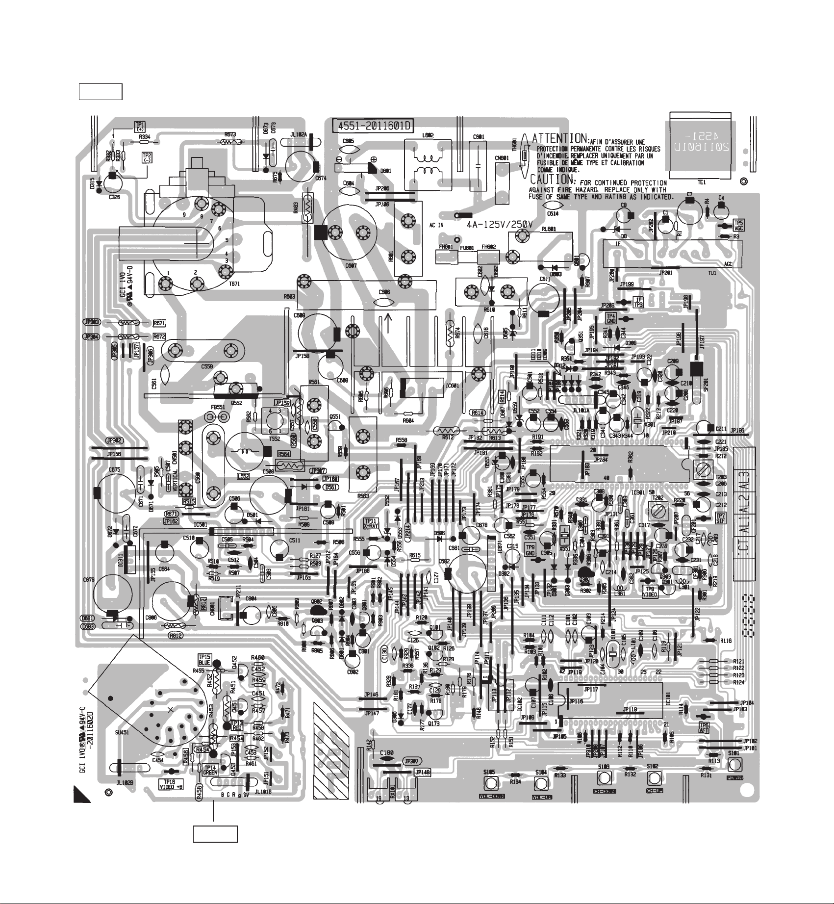
P.C. BOARDS
PCB-1
MAIN P.C. BOARD
PCB-2 CRT SOCKET P.C. BOARD
16
Page 18
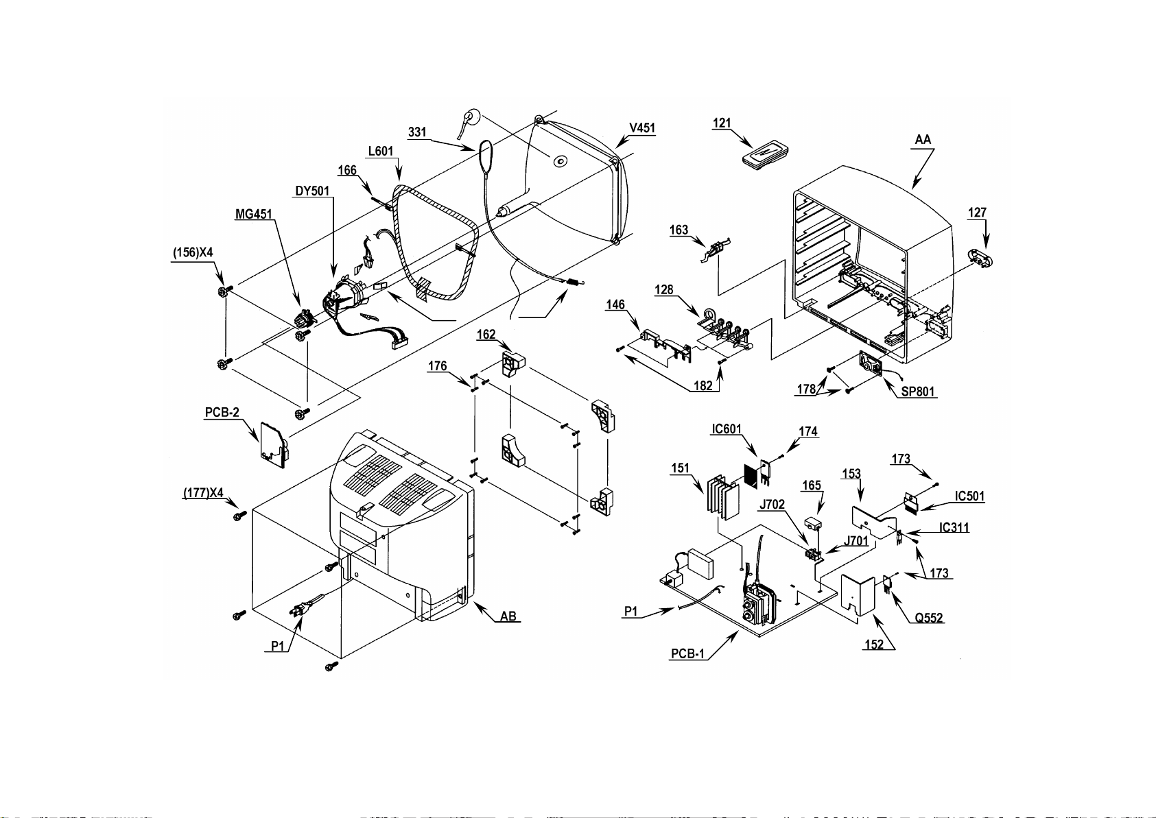
EXPLODED VIEW
142
158
- 16 -
Page 19
Ref No. Ref No.
Part No. Description Part No. Description
GENERAL UNIT PARTS LIST MISCELLANEOUS
127 1532-24801 Window;SENSOR 315 4291-034 Magnet Assembly
128 1662-78101 Push Button 315 4291-031 Magnet Assembly SUFFIX C
142 2132-412 Wedge Deflection Yoke;SPACER(x3) 315 4291-031 Magnet Assembly SUFFIX E
146 2133-314 Protector;BUTTON 331 4105-01102 CRT Wire;(CRT GND)
151 2222-379 Heat Sink;CA
152 2222-294 Heat Sink;CA
153 2222-302 Heat Sink;CA
156 2340-065 Screw (+);(x4) CAPACITORS
158 2651-0000199 Spring CRT;WIRE
161 2240-581 Holder C1 5345-106-50 10 uF +-20% 50V Electrolytic
162 2240-613 Holder;(x4) C4 5345-475-50 4.7 uF +-20% 50V Electrolytic
163 2240-742 Holder;CORD C7 5345-337-16 330 uF +-20% 16V Electrolytic
166 2240-7052 Holder Wiring C8 5345-226-50 22 uF +-20% 50V Electrolytic
167 2240-7051 Holder Wiring;DY L601/CRT WIRE,JL101 C101 5369-104144 0.1 uF +-10% 25V Semiconductor
168 2240-R0101 Holder Wiring; (x4) C102 5369-104144 0.1 uF +-10% 25V Semiconductor
173 2347-R0130082 Self-Tapping Screw (+) (3x8 mm);(x3);CA C103 5345-475-50 4.7 uF +-20% 50V Electrolytic
174 2347-R0130102 Self-Tapping Screw (+) (3x10 mm);(x12);CA C104 5361-270JCH 27 pF +-5% 50V Ceramic CH
176 2347-R0140162 Self-Tapping Screw (+) (4x16 mm); C105 5361-270JCH 27 pF +-5% 50V Ceramic CH
177 2347-R0140162 Self-Tapping Screw (+) (4x16 mm);BACK(x4) C106 5361-300JCH 30 pF +-5% 50V Ceramic CH
178 2347-R0130082 Self-Tapping Screw (+) (3x8 mm);(x2) C107 5345-107-10 100 uF +-20% 10V Electrolytic
182 2347-R0130102 Self-Tapping Screw(+)(3x10mm);314,BUTTONx3(x5) C108 V5369-S04FZ223 0.022 uF +80%-20% 25V Semiconductor
145 2133-313 Protector;SENSOR;AA C109 S5361-S17CJ8R2 8.2 pF +-5% 50V Ceramic CH
AA A412-19V1131A Cabinet C111 5361-681KB 680 pF +-10% 50V Semiconductor
AB A422-19V1131A Cabinet Back; SUFFIX A C112 5361-681KB 680 pF +-10% 50V Semiconductor
AB A422-19V1131B Cabinet Back; SUFFIX B C126 5361-561KB 560 pF +-10% 50V Ceramic B
AB A422-19V1131C Cabinet Back; SUFFIX E C127 5361-102KB 1000 pF +-10% 50V Semiconductor
AB A422-19V1131D Cabinet Back; SUFFIX D C129 5361-101KB 100 pF +-10% 50V Ceramic B
AB A422-19V1131E Cabinet Back; SUFFIX C C177 V5361-S17BK271 270 pF +-10% 50V Ceramic B
C180 V5361-S17BK101 100 pF +-10% 50V Ceramic B
PCB-1 MAIN P.C.BOARD
ELECTRICAL PARTS LIST C206 V5369-S05BK102 1000 pF +-10% 50V Semiconductor
COILS AND TRANSFORMER
L601 4994-040 Coil C210 V5369-S04FZ103 0.01 uF +80%-20% 25V Semiconductor
C208 5345-474-50 0.47 uF +-20% 50V Electrolytic
C209 5345-476-16 47 uF +-20% 16V Electrolytic
C211 5345-475-50 4.7 uF +-20% 50V Electrolytic
MISCELLANEOUS C212 5345-475-50 4.7 uF +-20% 50V Electrolytic
C213 V5369-S03XM472 4700 pF +-20% 16V Semiconductor
DY501 4993-118 Coil Deflection Yoke SUFFIX A C214 5361-103ZF 0.01 uF +80%-20% 25V Semiconductor
DY501 4993-060 Coil Deflection Yoke SUFFIX B C217 5361-470JCH 47 pF +-5% 50V Ceramic CH
DY501 4993-122 Coil Deflection Yoke SUFFIX C C218 5361-470JCH 47 pF +-5% 50V Ceramic CH
DY501 4993-119 Coil Deflection Yoke SUFFIX D C220 V5369-S03XM222 2200 pF +-20% 16V Semiconductor
DY501 4993-123 Coil Deflection Yoke SUFFIX E C221 V5369-S04FZ103 0.01 uF +80%-20% 25V Semiconductor
SP801 5812-0101G750 Speaker C231 V5369-S04FZ103 0.01 uF +80%-20% 25V Semiconductor
LCN801 4163-06038003 Connector with Lead Wire;(SP) C232 5345-476-16 47 uF +-20% 16V Electrolytic
V451 5721-015ST51N CRT;(51GGD95X) SUFFIX A C303 5354-104K1HM 0.1 uF +-5% 50V TF
V451 5721-51CN020T CRT;(510UEB22(DY)) SUFFIX B C304 V5369-S04FZ103 0.01 uF +80%-20% 25V Semiconductor
V451 5721-028TT48N CRT;(A48LRH93X) SUFFIX C C305 5345-105-50 1 uF +-20% 50V Electrolytic
V451 5721-029NT48N CRT;(A48LSD095X) SUFFIX D C306 5354-104K1HM 0.1 uF +-10% 50V Mylar
V451 5721-031ZT48N CRT;(A48LGS30X) SUFFIX E C308 5345-106-50 10 uF +-20% 50V Electrolytic
121 6142-09202 Infrared Remote Control;CONTROL
- 18 -
Page 20

Ref No. Ref No.
Part No. Description Part No. Description
CAPACITORS CAPACITORS
C315 5342-S06FM225 2.2 uF +-20% 50V Electrolytic NP C604 5361-S40FM103 0.01 uF +-20% 250V Cetamic F
C317 V5369-S04FZ103 0.01 uF +80%-20% 25V Semiconductor C605 5361-S40FM103 0.01 uF +-20% 250V Cetamic F
C318 5345-476-16 47 uF +-20% 16V Electrolytic C606 5361-S09VZ103 0.01 uF +80%-20% 250V Ceramic
C319 V5361-S17CJ100 10 pF +-5% 50V Ceramic CH C607 5341-S52LM477 470 uF +-20% 200V Electrolytic
C320 V5369-S04FZ223 0.022 uF +80%-20% 25V Semiconductor C608 5345-S59KM226 22 uF +-20% 160V Electrolytic
C322 5345-474-50 0.47 uF +-20% 50V Electrolytic C609 5345-S59KM336 33 uF +-20% 160V Electrolytic
C326 5345-105-250 1 uF +-20% 250V Electrolytic C611 5345-108-25 1000 uF +-20% 25V Electrolytic
C331 V5369-S04FZ103 0.01 uF +80%-20% 25V Semiconductor C614 5361-S40FM103 0.01 uF +-20% 250V Cetamic F
C341 5345-104-50 0.1 uF +-20% 50V Electrolytic C616 5361-S09VZ103 0.01 uF +80%-20% 250V Ceramic
C342 5345-104-50 0.1 uF +-20% 50V Electrolytic C664 5345-107-16 100 uF +-20% 16V Electrolytic
C343 5345-104-50 0.1 uF +-20% 50V Electrolytic C671 5359-3321959 3300 pF +-10% 400V Polypropylene
C344 V5361-S17BK101 100 pF +-10% 50V Ceramic B C672 5359-1031959 0.01 uF +-10% 400V Polypropylene
C345 V5361-S17BK101 100 pF +-10% 50V Ceramic B C673 5359-3321959 3300 pF +-10% 400V Polypropylene
C346 V5361-S17BK101 100 pF +-10% 50V Ceramic B C674 5345-106-250 10 uF +-20% 250V Electrolytic
C361 5354-102K1HM 1000 pF +-10% 50V Mylar C675 5345-108-35 1000 uF +-20% 35V Electrolytic
C362 V5361-S17BK101 100 pF +-10% 50V Ceramic B C676 5345-108-25 1000 uF +-20% 25V Electrolytic
C380 5345-105-50 1 uF +-20% 50V Electrolytic C678 5345-107-25 100 uF +-20% 25V Electrolytic
C381 V5369-S04FZ103 0.01 uF +80%-20% 25V Semiconductor C681 5354-104K1HM 0.1 uF +-10% 50V Mylar
C391 5345-105-50 1 uF +-20% 50V Electrolytic C682 5345-228-06 2200 uF +-20% 6.3V Electrolytic
C501 5345-L225M50 2.2 uF +-20% 50V Electrolytic L.L C801 5345-475-50 4.7 uF +-20% 50V Electrolytic
C503 5354-333K1HM 0.033 uF +-10% 50V Mylar C802 5345-476-16 47 uF +-20% 50V Electrolytic
C504 V5361-S17BK471 470 pF +-10% 50V Ceramic B C803 V5369-S03XM222 2200pF +-20% 16V Semiconductor
C505 5354-104K1HM 0.1 uF +-5% 50V TF C804 5345-227-16 220 uF +-20% 16V Electrolytic
C506 5345-107-35 100 uF +-20% 35V Electrolytic C805 5369-104144 0.1 uF +-10% 25V Semiconductor
C507 5354-473K1HM 0.047 uF +-10% 50V Mylar C806 5345-108-16 1000 uF +-20% 16V Electrolytic
C508 5345-108-35 1000 uF +-20% 35V Electrolytic
C509 5345-L225M50 2.2 uF +-20% 50V Electrolytic L.L RESISTORS
C510 5345-L335M50 3.3 uF +-20% 50V Electrolytic L.L
C511 5345-107-35 100 uF +-20% 35V Electrolytic R1 5134-221J25P 220 ohm +-5% 1/4W Carbon
C512 V5361-S17BK101 100 pF +-10% 50V Ceramic B R3 V5133-R010J103 10 k ohm +-5% 1/8W Carbon
C551 V5369-S04FZ103 0.01 uF +80%-20% 25V Semiconductor R4 V5133-R010J184 180 k ohm +-5% 1/8W Carbon
C552 5345-225-50 2.2 uF +-20% 50V Electrolytic R101 V5133-R010J472 4.7 k ohm +-5% 1/4W Carbon
C553 V5369-S04FZ103 0.01 uF +80%-20% 25V Semiconductor R102 V5133-R010J472 4.7 k ohm +-5% 1/4W Carbon
C554 5345-107-16 100 uF +-20% 16V Electrolytic R103 V5133-R010J101 100 ohm +-5% 1/4W Carbon
C555 5345-106-50 10 uF +-20% 50V Electrolytic R104 V5133-R010J101 100 ohm +-5% 1/4W Carbon
C556 5345-106-50 10 uF +-20% 50V Electrolytic R105 V5133-R010J102 1 k ohm +-5% 1/8W Carbon
C557 5361-R01BK681 680 pF +-10% 500V Ceramic R106 V5133-R010J223 22 k ohm +-5% 1/8W Carbon
C558 5361-R01BK561 560 pF +-10% 500V Ceramic R107 V5133-R010J223 22 k ohm +-5% 1/8W Carbon
C559 5352-S020J822 8200 pF +-5% 1.6 kV Metalized Polyester R110 V5133-R010J223 22 k ohm +-5% 1/8W Carbon
C560 5352-S261J474 0.47 uF +-5% 200V Metalized Polyester R112 V5133-R010J223 22 k ohm +-5% 1/8W Carbon
C561 5361-S11BK102 1000 pF +-10% 2 kV Ceramic; SUFFIX A R113 V5133-R010J103 10 k ohm +-5% 1/8W Carbon
C561 5361-S11BK681 680 pF +-10% 2 kV Ceramic; SUFFIX C R114 V5133-R010J102 1 k ohm +-5% 1/8W Carbon
C561 5361-S11BK102 1000 pF +-10% 2 kV Ceramic; SUFFIX D R116 V5133-R010J102 1 k ohm +-5% 1/8W Carbon
C562 5345-105-50 1 uF +-20% 50V Electrolytic R119 5134-102J25P 1 k ohm +-5% 1/4W Carbon
C601 5352-S331K104 0.1uF+-10% Metalized Polyester R120 V5133-R010J102 1 k ohm +-5% 1/4W Carbon
C602 5361-S40FM103 0.01 uF +-20% 250V Cetamic F R121 5134-562J25P 5.6 k ohm +-5% 1/4W Carbon
R122 5134-562J25P 5.6 k ohm +-5% 1/4W Carbon
R123 5134-562J25P 5.6 k ohm +-5% 1/4W Carbon
- 19 -
Page 21
Ref No. Ref No.
Part No. Description Part No. Description
RESISTORS RESISTORS
R124 5134-562J25P 5.6 k ohm +-5% 1/4W Carbon R335 5232-124J16P 120 k ohm +-5% 1/6W Carbon
R126 V5133-R010J223 22 k ohm +-5% 1/8W Carbon R336 V5133-R010J222 2.2 k ohm +-5% 1/8W Carbon
R127 5134-274J25P 270 k ohm +-5% 1/4W Carbon R340 V5133-R010J105 1 M ohm +-5% 1/8W Carbon
R128 5232-222J16P 2.2 k ohm +-5% 1/6W Carbon R341 V5133-R010J821 820 ohm +-5% 1/8W Carbon
R129 V5133-R010J103 10 k ohm +-5% 1/8W Carbon R342 V5133-R010J821 820 ohm +-5% 1/8W Carbon
R131 V5133-R010J332 3.3 k ohm +-5% 1/8W Carbon R343 V5133-R010J821 820 ohm +-5% 1/8W Carbon
R132 V5133-R010J332 3.3 k ohm +-5% 1/8W Carbon R344 V5133-R010J103 10 k ohm +-5% 1/8W Carbon
R133 V5133-R010J562 5.6 k ohm +-5% 1/8W Carbon R350 V5133-R010J471 470 ohm +-5% 1/8W Carbon
R134 V5133-R010J123 12 k ohm +-5% 1/8W Carbon R351 V5133-R010J221 220 ohm +-5% 1/8W Carbon
R136 V5133-R010J104 100 k ohm +-5% 1/8W Carbon R361 5134-102J25P 1 k ohm +-5% 1/4W Carbon
R137 V5133-R010J153 15 k ohm +-5% 1/8W Carbon R362 V5133-R010J393 39K ohm +-5% 1/8W Carbon
R142 5134-102J25P 1 k ohm +-5% 1/4W Carbon R381 5135-821J50P 820 ohm +-5% 1/2W Carbon
R146 V5133-R010J102 1 k ohm +-5% 1/8W Carbon R391 V5133-R010J753 75 k ohm +-5% 1/8W Carbon
R151 5134-102J25P 1 k ohm +-5% 1/4W Carbon R463 5102-S141J2R2 2.2 ohm +-5% 2W Fuse;SUFFIX A
R152 5134-102J25P 1 k ohm +-5% 1/4W Carbon R463 5102-S141J2R7 2.7 ohm +-5% 2W Fuse;SUFFIX B
R176 5134-103J25P 10 k ohm +-5% 1/4W Carbon R463 5102-S141J5R6 5.6 ohm +-5% 2W Fuse;SUFFIX C
R177 V5133-R010J333 33 k ohm +-5% 1/8W Carbon R463 5102-S141J2R7 2.7 ohm +-5% 2W Fuse;SUFFIX D
R178 V5133-R010J563 56 k ohm +-5% 1/8W Carbon R463 5102-S141J5R6 5.6 ohm +-5% 2W Fuse;SUFFIX E
R179 5134-183J25P 18 k ohm +-5% 1/4W Carbon R501 V5133-R010J102 1 k ohm +-5% 1/8W Carbon
R180 5232-683J16P 68 k ohm +-5% 1/6W Carbon R503 5134-101J25P 100 ohm +-5% 1/4W Carbon
R181 V5133-R010J333 33 k ohm +-5% 1/8W Carbon R504 V5133-R010J153 15 k ohm +-5% 1/8W Carbon
R191 V5133-R010J102 1 k ohm +-5% 1/8W Carbon R505 5134-391J25P 390 ohm +-5% 1/4W Carbon
R192 V5133-R010J102 1 k ohm +-5% 1/8W Carbon R507 V5133-R010J563 56 k ohm +-5% 1/8W Carbon
R212 V5133-R010J103 10 k ohm +-5% 1/8W Carbon R508 V5133-R010J333 33 k ohm +-5% 1/8W Carbon
R213 V5133-R010J391 390 ohm +-5% 1/8W Carbon R509 5135-1R8J50P 1.8 ohm +-5% 1/2W Carbon
R214 V5133-R010J563 56 k ohm +-5% 1/8W Carbon R510 V5133-R010J562 5.6 k ohm +-5% 1/8W Carbon
R218 V5133-R010J102 1 k ohm +-5% 1/8W Carbon R515 5134-222J25P 2.2 k ohm +-5% 1/4W Carbon
R220 V5133-R010J102 1 k ohm +-5% 1/8W Carbon R518 5232-183J16P 18 k ohm +-5% 1/6W Carbon
R301 V5133-R010J182 1.8 k ohm +-5% 1/8W Carbon R518 5232-223J16P 22 k ohm +-5% 1/6W Carbon; SUFFIX E
R302 V5133-R010J182 1.8 k ohm +-5% 1/8W Carbon R518 5232-153J16P 15 k ohm +-5% 1/6W Carbon; SUFFIX D
R303 5134-182J25P 1.8 k ohm +-5% 1/4W Carbon R518 5232-153J16P 15 k ohm +-5% 1/6W Carbon; SUFFIX C
R305 V5133-R010J332 3.3 k ohm +-5% 1/8W Carbon R519 5232-473J16P 47 k ohm +-5% 1/6W Carbon; SUFFIX D
R306 V5133-R010J331 330 ohm +-5% 1/8W Carbon R519 5232-822J16P 8.2 k ohm +-5% 1/6W Carbon; SUFFIX C
R307 V5133-R010J331 330 ohm +-5% 1/8W Carbon R551 5134-222J25P 2.2 k ohm +-5% 1/4W Carbon
R308 V5133-R010J102 1 k ohm +-5% 1/8W Carbon R554 V5133-R010J473 47 k ohm +-5% 1/8W Carbon
R319 V5133-R010J221 220 ohm +-5% 1/8W Carbon R555 V5133-R010J153 15 k ohm +-5% 1/8W Carbon
R320 V5133-R010J221 220 ohm +-5% 1/8W Carbon R556 V5133-R010J562 5.6 k ohm +-5% 1/8W Carbon
R321 V5133-R010J221 220 ohm +-5% 1/8W Carbon R557 V5133-R010J102 1 k ohm +-5% 1/8W Carbon
R322 V5133-R010J332 3.3 k ohm +-5% 1/8W Carbon R558 V5133-R010J331 330 ohm +-5% 1/8W Carbon
R328 V5133-R010J222 2.2 k ohm +-5% 1/8W Carbon R559 V5133-R010J331 330 ohm +-5% 1/8W Carbon
R329 V5133-R010J562 5.6 k ohm +-5% 1/8W Carbon R561 5275-S080K222 2.2 k ohm +-10% 5W Cement
R330 V5133-R010J224 220 k ohm +-5% 1/8W Carbon R562 5135-0R5J50P 0.5 ohm +-5% 1/2W Carbon
R331 5232-394J16P 390 k ohm +-5% 1/6W Carbon R563 5275-S080K221 220 ohm +-10% 5W Cement
R332 5134-102J25P 1 k ohm +-5% 1/4W Carbon R564 5102-6815711 680 ohm +-5% 1W Fuse
R333 5135-124J50P 120 k ohm +-5% 1/2W Carbon R570 V5133-R010J391 390 ohm +-5% 1/8W Carbon
R334 5135-124J50P 120 k ohm +-5% 1/2W Carbon R601 5275-S080K2R7 2.7 ohm +-10% 5W Cement
- 20 -
Page 22
Ref No. Ref No.
Part No. Description Part No. Description
RESISTORS INTEGRATED CIRCUITS
R603 5277-271591 270 ohm 15W Cement IC101 5654-TA87C-B2 IC;(u-COM)
R604 5171-S071J123 12 k ohm +-5% 1W Metal IC102 5654-M24C02B IC;(EEPROM)
R605 5134-334J25P 330 k ohm +-5% 1/4W Carbon IC301 5653-TA1268N IC, TA1268N ;(IF/VIDEO/CHROMA/DEF)
R606 5102-S101J470 47 ohm +-5% 1/4W Fuse IC311 5653-NJ7809FA IC, NJM7809FA;(9V REGULATOR)
R607 V5133-R010J472 4.7 k ohm +-5% 1/8W Carbon IC501 5652-AN5512 IC, AN5512;(VERTICAL)
R610 5275-S080K152 1.5 k ohm +-10% 5W Cement IC601 5653-STR30130 IC, STR30130;(AVR)
R611 5135-681J50P 680 ohm +-5% 1/2W Carbon IC671 5653-NJ7805LD IC, NJM78LR05L-D;(5V REGULATOR/RESET 4.2V)
R612 5173-S051J392 3.9 k ohm +-5% 2W Metal
R613 5173-S051J392 3.9 k ohm +-5% 2W Metal DIODES
R614 5134-681J25P 680 ohm +-5% 1/4W Carbon
R615 5134-470J25P 47 ohm +-5% 1/4W Carbon D8 5635-HZT33 Zener, HZT33 33V 400mW
R671 5102-2R25720 2.2 ohm +-5% 1W Fuse D301 5636-1S2473 Diode,1S2473
R672 5102-2R25720 2.2 ohm +-5% 1W Fuse D302 5636-1SS133 Diode,1SS133
R673 5102-S101J2R2 2.2 ohm +-5% 1/4W Fuse D303 5636-1S2473 Diode,1S2473
R674 5171-S071J183 18 k ohm +-5% 1W Metal D306 5636-1SS133 Diode,1SS133
R675 V5133-R010J105 1 M ohm +-5% 1/8W Carbon D308 5636-1S2473 Diode,1S2473
R801 V5133-R010J471 470 ohm +-5% 1/8W Carbon D309 5636-1SS133 Diode,1SS133
R802 V5133-R010J103 10 k ohm +-5% 1/8W Carbon D310 5636-1SS133 Diode,1SS133
R803 V5133-R010J102 1 k ohm +-5% 1/8W Carbon D311 5636-1SS133 Diode,1SS133
R804 V5133-R010J103 10 k ohm +-5% 1/8W Carbon D312 5636-1SS133 Diode,1SS133
R805 V5133-R010J471 470 ohm +-5% 1/8W Carbon D315 5636-1SS133 Diode,1SS133
R806 V5133-R010J151 150 ohm +-5% 1/8W Carbon D501 5632-1N4002E Diode, RL1N4002-E
R807 V5133-R010J151 150 ohm +-5% 1/8W Carbon D552 5635-RD6R8ES2 Zener;6.8V
R808 5232-1R0J16P 1 ohm +-5% 1/6W Carbon D553 5636-1SS133 Diode,1SS133
R809 5232-2R2J16P 2.2 ohm +-5% 1/6W Carbon D554 5636-1SS133 Diode,1SS133
R810 V5133-R010J2R2 2.2 ohm +-5% 1/8W Carbon D555 5635-RD3R3ES2 Zener;3.3V
R812 5102-S111J100 10 ohm +-5% 1/2W Fuse D559 5635-RD9R1ES2 Zener;9.1V
D601 5685-RS204LST Bridge Silicon Diode
TRANSISTORS D602 5632-1N4004E Diode, RL1N4004-E
D603 5632-1N4002E Diode, RL1N4002-E
Q101 5613-C143ZS Transistor, DTC143ZS D605 5635-RD8R2ES2 Zener;8.2V
Q102 5613-945(P) Transistor, 2SC945(P) D606 5636-1S2473 Diode,1S2473
Q173 5613-945(P) Transistor, 2SC945(P) D607 5636-1SS133 Diode, 1SS133
Q301 5613-945(P) Transistor, 2SC945(P) D671 5632-1F4-E Diode, 1F4
Q302 5611-733(P) Transistor, 2SA733(P) D672 5632-1F4-E Diode, 1F4
Q303 5613-945(P) Transistor, 2SC945(P) D673 5632-1F4-E Diode, 1F4
Q351 5613-C143ZS Transistor, DTC143ZS D701 5632-1F4-E Diode, 1F4
Q551 5613-1473A(R) Transistor, 2SC1473A(R) D702 5636-1N4148M Diode,1N4148M
Q552 5614-1877 Transistor, 2SD1877;(HORIZONTAL) D703 5636-1N4148M Diode,1N4148M
Q601 5613-945(P) Transistor, 2SC945(P) D801 5636-1SS133 Diode, 1SS133
Q801 5613-945(P) Transistor, 2SC945(P) D802 5636-1SS133 Diode, 1SS133
Q802 5611-950(O) Transistor, 2SA950(O)
Q803 5613-2120(O) Transistor, 2SC2120(O) COILS AND TRANSFORMERS
L101 5995-470098 Coil 47 uH
L203 5995-220098 Coil 22 uH
L301 5995-150098 Coil 15 uH
L361 5995-5R6098 Coil 5.6 uH
- 21 -
Page 23
Note:
Ref No. Ref No.
Part No. Description Part No. Description
COILS AND TRANSFORMERS
L552 5995-540084 Coil;(LINEARITY) CAPACITORS
L602 5583-52301 Coil AF CH;(LINE FILTER)
T202 5932-12502 Coil;(AFT) C451 5361-681KB 680 pF +-10% 50V Ceramic B
T203 5562-0019 Transformer SIF Det.;(SIF DET) C452 5361-561KB 560 pF +-10% 50V Ceramic B
T552 5581-18801 Transformer C453 5361-681KB 680 pF +-10% 50V Ceramic B
T671 4992-078 Transformer; SUFFIX A,B,D C454 5361-S11BK102 1000 pF +-10% 2 kV Ceramic
T671 4992-091 Transformer; SUFFIX E
T671 4992-091 Transformer; SUFFIX C RESISTORS
PCB-2 CRT SOCKET P.C.BOARD(D551-19V1114B)
MISCELLANEOUS R451 5171-S071J153 15 k ohm +-5% 1W Metal
R452 5171-S071J153 15 k ohm +-5% 1W Metal
CF201 5671-02810452 Ceramic Filter;(4.5MHz BAND PASS F.) R453 5171-S071J153 15 k ohm +-5% 1W Metal
CF301 5671-02410452 Ceramic Filter;(4.5MHz TRAP) R454 5135-332J50P 3.3 k ohm +-5% 1/2W Carbon
CN501 4443-0501142 Connector 5-pin;(DY) R455 5135-332J50P 3.3 k ohm +-5% 1/2W Carbon
CN601 4443-10101002 Connector 2-pin.;(DEGAUSS) R456 5135-332J50P 3.3 k ohm +-5% 1/2W Carbon
CN801 4443-03201003 Connector;(SP) R457 5232-271J16P 270 ohm +-5% 1/6W Carbon
FB551 5597-51001 Ferrite Bead R458 5134-122J25P 1.2 k ohm +-5% 1/4W Carbon
FH601 4472-05001 Fuse Holder;(FU601) R459 5232-271J16P 270 ohm +-5% 1/6W Carbon
FH602 4472-05001 Fuse Holder;(FU601) R460 5134-122J25P 1.2 k ohm +-5% 1/4W Carbon
FU601 5732-02401402 Fuse;(4A/125V) R461 5232-271J16P 270 ohm +-5% 1/6W Carbon
JL101 4242-R0505401 Jumper Lead 5-Wire;(MAIN~CRT) R462 5134-122J25P 1.2 k ohm +-5% 1/4W Carbon
JL102 4242-R0504351 Jumper Lead 4-Wire;(MAIN~CRT) R471 V5133-R010J221 220 ohm +-5% 1/8W Carbon
P1 4161-14701212 Cord w/Plug;(AC CORD) R472 V5133-R010J221 220 ohm +-5% 1/8W Carbon
RL601 4331-03401 DC Relay R473 V5133-R010J221 220 ohm +-5% 1/8W Carbon
RX101 6143-02401 Remote Control Receiver Unit
S101 4437-0611 Push Switch TRANSISTORS
S102 4437-0611 Push Switch
S103 4437-0611 Push Switch Q451 5613-1573A(R) Transistor, 2SC1573A(R)
S104 4437-0611 Push Switch Q452 5613-1573A(R) Transistor, 2SC1573A(R)
S105 4437-0611 Push Switch Q453 5613-1573A(R) Transistor, 2SC1573A(R)
SF201 5679-01501450 Surface Acoustic Wave Filter
TE1 4363-01201 Antenna Coupler;(ANT) MISCELLANEOUS
TH601 5192-01101 Posistor
TU1 6119-15501 VHF/UHF/CATV Tuner Assembly SU451 4474-08101 Socket; SUFFIX A,B,D
X101 5691-S1903802 Crystal Osc.8.0MHz SU451 4474-08001 Socket; SUFFIX E
X301 5691-S1901362 Crystal Osc. 3.579545MHz SU451 4474-08001 Socket; SUFFIX C
X551 5693-SB503F30 Ceramic Osc. 503 kHz
Safety Related Components.
Use Only Exact Replacement Parts.
- 22 -
 Loading...