

Page 1

MT1098
SERVICE MANUAL
COLOR TELEVISION RECEIVER
ORIGINAL
MFR’S VERSION B
Design and specifications are subject to change without notice.
Page 2
SERVICING NOTICES ON CHECKING
As for the places which need special attentions,
they are indicated with the labels or seals on the
cabinet, chassis and parts. Make sure to keep the
indications and notices in the operation manual.
2. AVOID AN ELECTRIC SHOCK
There is a high voltage part inside. Avoid an
electric shock while the electric current is
flowing.
3. USE THE DESIGNATED PARTS
The parts in this equipment have the specific
characters of incombustibility and withstand
voltage for safety. Therefore, the part which is
replaced should be used the part which has
the same character.
Especially as to the important parts for safety
which is indicated in the circuit diagram or the
table of parts as a mark, the designated
parts must be used.
PUT PARTS AND WIRES IN THE
4.
ORIGINAL POSITION AFTER
ASSEMBLING OR WIRING
There are parts which use the insulation
material such as a tube or tape for safety, or
which are assembled in the condition that
these do not contact with the printed board.
The inside wiring is designed not to get closer
to the pyrogenic parts and high voltage parts.
Therefore, put these parts in the original
positions.
5. TAKE CARE TO DEAL WITH THE
CATHODE-RAY TUBE
In the condition that an explosion-proof cathoderay tube is set in this equipment, safety is
secured against implosion. However, when
removing it or serving from backward, it is
dangerous to give a shock. Take enough care to
deal with it.
6. AVOID AN X-RAY1. KEEP THE NOTICES
Safety is secured against an X-ray by considering about the cathode-ray tube and the high
voltage peripheral circuit, etc.
Therefore, when repairing the high voltage peripheral circuit, use the designated parts and
make sure not modify the circuit.
Repairing except indicates causes rising of high
voltage, and it emits an X-ray from the cathoderay tube.
7.PERFORM A SAFETY CHECK AFTER
SERVICING
Confirm that the screws, parts and wiring which
were removed in order to service are put in the
original positions, or whether there are the
portions which are deteriorated around the
serviced places serviced or not. Check the
insulation between the antenna terminal or
external metal and the AC cord plug blades.
And be sure the safety of that.
(INSULATION CHECK PROCEDURE)
1.
Unplug the plug from the AC outlet.
2.
Remove the antenna terminal on TV and turn
on the TV.
3.
Insulation resistance between the cord plug
terminals and the eternal exposure metal
[Note 2] should be more than 1M ohm by
using the 500V insulation resistance meter
[Note 1].
4.
If the insulation resistance is less than 1M
ohm, the inspection repair should be
required.
[Note 1]
If you have not the 500V insulation
resistance meter, use a Tester.
[Note 2]
External exposure metal: Antenna terminal
Earphone jack
HOW TO ORDER PARTS
Please include the following informations when you order parts. (Particularly the VERSION LETTER.)
1. MODEL NUMBER and VERSION LETTER
The MODEL NUMBER can be found on the back of each product and the VERSION LETTER can be
found at the end of the SERIAL NUMBER.
2. PART NO. and DESCRIPTION
You can find it in your SERVICE MANUAL.
IMPORTANT
Inferior silicon grease can damage IC's and transistors.
When replacing an IC's or transistors, use only specified silicon grease (YG6260M).
Remove all old silicon before applying new silicon.
A1-1
Page 3

CONTENTS
SERVICING NOTICES ON CHECKING ..........................................................................................................
HOW TO ORDER PARTS................................................................................................................................
IMPORTANT....................................................................................................................................................
CONTENTS......................................................................................................................................................
GENERAL SPECIFICATIONS.........................................................................................................................
DISASSEMBLY INSTRUCTIONS
1. REMOVAL OF ANODE CAP.................................................................................................................
2. REMOVAL OF DEFLECTION YOKE.....................................................................................................
3. REMOVAL AND INSTALLATION OF FLAT PACKAGE IC....................................................................
SERVICE MODE LIST .....................................................................................................................................
CONFIRMATION OF HOURS USED..............................................................................................................
WHEN REPLACING EEPROM (MEMORY) IC...............................................................................................
ELECTRICAL ADJUSTMENTS.......................................................................................................................
MAJOR COMPONENTS LOCATION GUIDE..................................................................................................
BLOCK DIAGRAM...........................................................................................................................................
PRINTED CIRCUIT BOARDS
MAIN/CRT..............................................................................................................................................
SCHEMATIC DIAGRAMS
MICON/TUNER.....................................................................................................................................
CHROMA ..............................................................................................................................................
DEFLECTION/CRT................................................................................................................................
POWER.................................................................................................................................................
AV/SOUND ...........................................................................................................................................
WAVEFORMS..................................................................................................................................................
MECHANICAL EXPLODED VIEW..................................................................................................................
MECHANICAL REPLACEMENT PARTS LIST...............................................................................................
ELECTRICAL REPLACEMENT PARTS LIST.................................................................................................
A1-1
A1-1
A1-1
A2-1
A3-1~A3-4
B1-1
B2-1
B3-1, B3-2
C-1
C-1
C-1
D1-1~D2-1
D3-1
E-1, E-2
F-1~F-4
G-1, G-2
G-3, G-4
G-5, G-6
G-7, G-8
G-9, G-10
H-1, H-2
I-1
J1-1
J2-1, J2-2
A2-1
Page 4
GENERAL SPECIFICATIONS
G-1.Outline of the Product
9 inch(222.8mmV):Measured diagonally
Color CRT 90 degree deflection
G-2.Broadcasting System
US System M
G-3.Color System NTSC PAL SECAM or Monochrome signal
G-4.NTSC Playback(PAL 60Hz) Yes No Not Applicable
G-5.NTSC 3.58+4.43/PAL60Hz Yes No Not Applicable
G-6.Antenna Input Impedance
VHF/UHF 75 ohm unbalanced
G-7.Tuner and Receiving Contactless Electric tuner 1Tuner System
2Tuner System
channel Tuner Oscar(W/O HYPER) Oscar(W/ HYPER)
France CATV) Others
Receiving channel
(USA) 2-69 , 4A , A-5~A-1 , A~I , J~W , W+1~W+84
Tuning System
Frequency syn. Voltage syn. Others
G-8.Preset Channel
-- channels
G-9.Intermediate Frequency
Picture(fP) 45.75MHz MHz MHz
Sound (fS) 41.25 MHz MHz MHz
fP-fS 4.50 MHz MHz MHz
G-10.Stereo/Dual TV Sound
Yes( NICAM GERMAN USA JAPAN) No
G-11.Tuner Sound Muting Yes No
G-12.Power Source DC 12 V
G-13.Power Consumption: 35 W at DC 12 V
Stand by: 1 W at DC 12 V
Per Year: -- kWh / Year
G-14.Dimensions(Approx.)
232 mm(W) 289 mm(D) 224 mm(H)
G-15.Weight(Approx.) Net : 5.0 kg ( 11.0 lbs)
Gross: 6.0 kg ( 13.2 lbs)
G-16.Cabinet Material
Cabinet Front: PS 94HB DECABROM
ABS 94V2 NON-DECA
94V0
Back Panel: PS 94HB DECABROM
ABS 94V2 NON-DECA
94V0
G-17.Protector: Power Fuse
A3-1
Page 5
GENERAL SPECIFICATIONS
G-18.Regulation
Safety
UL CSA SAA SI CE SEV
BS NF NEMKO FEMKO DEMKO IEC65
SEMKO NZ HOMOLO SABS CNS SISIR
NOM AS3159 DENTORI UNE GOST NONE
Radiation
FCC DOC FTZ PTT CE SEV
SABA SI NF NZ HOMOLO UNE
CNS CISPR13 DENTORI AS/NZS NONE
X-Radiation
PTB DHHS HWC DENTORI NONE
G-19.Temperature : Operation 5 ºC ~ 40 ºC
Storage -20 ºC ~ 60 ºC
G-20.Operating Humidity Less than 80 %RH
G-21.Clock and Timer
Sleep Timer Yes Max 120 Min.( 10 Min. Step) No
On/Off Timer Yes Programs No
Wake Up Timer Yes Programs No
G-22.Timer back up Time: More than -- Minutes (at Power Off Mode)
G-23.Terminals
VHF/UHF Antenna Input Din Type F-Type France Type
Front Video Input (RCA ø8.3)
Front Audio Input (RCA ø8.3)
Rear Video Input1 (RCA ø8.3)
Rear Audio Input1 (RCA ø8.3)
Rear Video Input2 (RCA ø8.3)
Rear Audio Input2 (RCA ø8.3)
Rear Video Output (RCA ø8.3)
Rear Audio Output (RCA ø8.3)
21 Pin DC Jack(Center +) Ear Phone Jack(ø3.5)
Head Phone Jack(ø3.5) AC Outlet Ext Speaker(ø3.5)
Diversity S Input(Front) S Input(Rear)
G-24.Indicator : Power Stand By On Timer NONE
( ) ( ) ( )
G-25.Display
On Screen Display
Menu Clock Set( 12H 24H)
CH Set TV/CATV
Auto Ch Memory
ADD/Delete
Picture
Language
V-Chip
Control Level Sound Brightness Contrast
Color Tint(NTSC Only) Sharpness
Tuning Bass Treble
Balance Back Light
Stereo,Audio Output,SAP Mid Night Theater
Stereo,Audio Output GAME Picture Menu
AV Channel Clock Hotel Lock
Sleep Timer Sound Mute Pin Code
A3-2
Page 6
GENERAL SPECIFICATIONS
G-26.OSD Language
Eng Ger Fre Spa Ita Por Jpn
OSD Language Setting
Eng Ger Fre Spa Ita Por Jpn
Not Applicable
G-27.Speaker NONE
Layout Front Side Bottom
Size/Quantity inches x pcs
Imp. ohm
Power Max. W
10 % W (Typical)
G-28.EXT Speaker : Yes No
Imp. 8 ohm
Power Max. 1.2 W
10 % 0.8 W (Typical)
G-29.Carton
Master Carton: Need No Need
Content: ---- Set
Material: ---- / ---- Corrugated Carton
Dimensions: ---- mm(L) ---- mm(W) ---- mm(D)
Description of Origin Yes No
Gift Box
Material Single/Brown Corrugated Carton ( with Photo Label)
Double/White Corrugated Carton ( with Photo Label)
Double Full Color Carton W/Photo
Dimensions: 294 mm(W) 348 mm(D) 295 mm(H)
Design: As Per Buyer 's
Description of Origin: Yes No
Drop Test Natural Dropping At 1 Corner / 3 Edges / 6 Surfaces
Height 25cm 31cm 46cm 62cm 80cm
Container Stuffing: 2,140 Sets / 40' container
G-30.Accessories
Owner's Manual ( W/Guarantee Card) [English/Spanish]
AC Plug Adapter Channel film
Battery (UM- x ) Remote Control Unit
Safety Tip Toll Free Insert Sheet
Guarantee Card Audio-Video Cord (RCA)
Registration Card Warning Sheet
Quick Set-Up Sheet Schematic Diagram
Information Sheet U/V Mixer
75 ohm Coaxial Cable ( Single Shield Double Shield)
300 ohm to 75 ohm VHF Antenna Adaptor
21pin Cable Car Cord
Rod Antenna
One Pole Two Pole( F-Type Din Type France Type)
Loop Antenna ( F-Type Din Type France Type)
G-31.Other Features
Auto Degauss Auto CH Memory
Auto Shut Off Picture Me nu
SAP Comb Filter
CATV(181CH) Game Position
Anti-Theft Mid Night Theater
Rental
Closed Caption V-Chip
A3-3
Page 7
GENERAL SPECIFICATIONS
G-32.Switch
Front
Power Channel Up/Reset Volume Up/Set+
System Select Channel Down/Enter Volume Down/SetMain Power SW Sub Power Menu
TV/AV Picture
Rear
AC/DC TV/CATV Selector
Degauss Main Power SW
G-33.Magnetic Field
BV: +0.45G BV: +0.35G BV: +0.25G
BH: 0.18G BH: 0.30G BH: 0.30G
BV: -0.15G BV: -0.25G BV: -0.50G
BH: 0.15G BH: 0.15G BH: 0.30G
G-34.Remote Control Unit: RC-CX
Power Source: D.C 3 V Battery UM - 4 x 2
Total 34 Keys
<CTV Control Keys>
CTV Power TV/AV
0 Volume Up
1 Volume Down
2 CH Up
3 CH Down
4 Sleep
5 Call
6 Reset
7 Enter
8 Menu
9 Set +
Quick View Set -
<VP Control Keys>
VP POWER Still
Play Repeat
Stop ATR
F.FWD Tr+
Rew Tr-
A3-4
Page 8
DISASSEMBLY INSTRUCTIONS
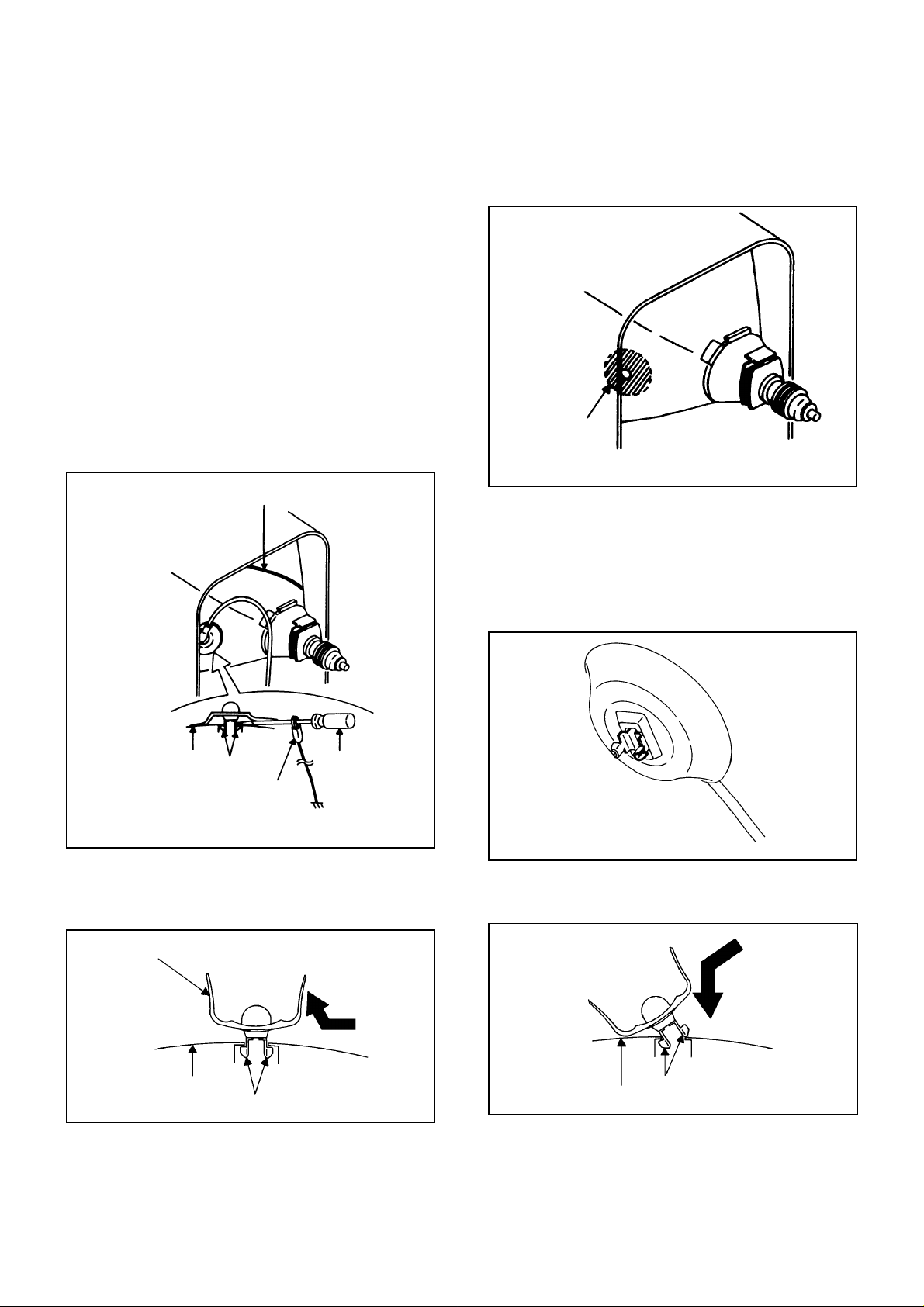
1. REMOVAL OF ANODE CAP
Read the following NOTED items before starting work.
After turning the power off there might still be a potential
*
voltage that is very dangerous. When removing the
Anode Cap, make sure to discharge the Anode Cap's
potential voltage.
Do not use pliers to loosen or tighten the Anode Cap
*
terminal, this may cause the spring to be damaged.
REMOVAL
Follow the steps as follows to discharge the Anode Cap.
1.
(Refer to Fig. 1-1.)
Connect one end of an Alligator Clip to the metal part of a
flat-blade screwdriver and the other end to ground.
While holding the plastic part of the insulated Screwdriver,
touch the support of the Anode with the tip of the
Screwdriver.
A cracking noise will be heard as the voltage is discharged.
GND on the CRT
INSTALLATION
Clean the spot where the cap was located with a small
1.
amount of alcohol. (Refer to Fig. 1-3.)
Location of Anode Cap
NOTE
Confirm that there is no dirt, dust, etc. at the spot where
the cap was located.
Arrange the wire of the Anode Cap and make sure the
2.
wire is not twisted.
Turn over the Rubber Cap. (Refer to Fig. 1-4.)
3.
Fig. 1-3
CRT
Support
Alligator Clip
Screwdriver
GND on the CRT
Fig. 1-1
Flip up the sides of the Rubber Cap in the direction of the
2.
arrow and remove one side of the support.
(Refer to Fig. 1-2.)
Rubber Cap
CRT
Support
Fig. 1-2
3. After one side is removed, pull in the opposite direction to
remove the other.
NOTE
Take care not to damage the Rubber Cap.
Fig. 1-4
4. Insert one end of the Anode Support into the anode button,
then the other as shown in Fig. 1-5.
Support
CRT
Fig. 1-5
5.6.Confirm that the Support is securely connected.
Put on the Rubber Cap without moving any parts.
B1-1
Page 9
DISASSEMBLY INSTRUCTIONS
2. REMOVAL OF DEFLECTION YOKE
(Refer to Fig. 2-1)
1.
Loosen the screw 1.
2.
Remove the Convergence • Purity Magnet in the
direction of arrow (A).
3.
Remove the 3 Wedges.
4.
Remove the Deflection Yoke in the direction of arrow
(A).
INSTALLATION
Install new Deflection Yoke in reverse steps of REMOVAL.
NOTE
After adjusting the purity and the convergence, fix the
screw 1 and lock the wedges.
Wedge
Wedge
(A)
Deflection Yoke
1
Convergence •
Purity Magnet
Fig. 2-1
B2-1
Page 10
DISASSEMBLY INSTRUCTIONS
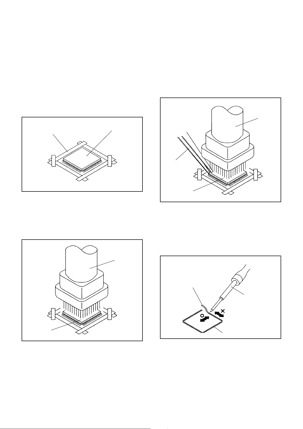
3.
REMOVAL AND INSTALLATION OF
FLAT PACKAGE IC
REMOVAL
Put the Masking Tape (cotton tape) around the Flat
1.
Package IC to protect other parts from any damage.
(Refer to Fig. 3-1.)
NOTE
Masking is carried out on all the parts located within
10 mm distance from IC leads.
When IC starts moving back and forth easily after
3.
desoldering completely, pickup the corner of the IC using
a tweezers and remove the IC by moving with the IC
desoldering machine. (Refer to Fig. 3-3.)
NOTE
Some ICs on the PCB are affixed with glue, so be
careful not to break or damage the foil of each IC
leads or solder lands under the IC when removing it.
Blower type IC
desoldering
machine
Masking Tape
(Cotton Tape)
Heat the IC leads using a blower type IC desoldering
2.
IC
machine. (Refer to Fig. 3-2.)
NOTE
Do not add the rotating and the back and forth
directions force on the IC, until IC can move back and
forth easily after desoldering the IC leads completely.
Blower type IC
desoldering machine
Fig. 3-1
Tweezers
IC
Fig. 3-3
Peel off the Masking Tape.4.
Absorb the solder left on the pattern using the Braided
5.
Shield Wire. (Refer to Fig. 3-4.)
NOTE
Do not move the Braided Shield Wire in the vertical
direction towards the IC pattern.
Braided Shield Wire
Soldering Iron
IC
Fig. 3-2
IC pattern
Fig. 3-4
B3-1
Page 11

DISASSEMBLY INSTRUCTIONS
INSTALLATION
Take care of the polarity of new IC and then install the
1.
new IC fitting on the printed circuit pattern. Then solder
each lead on the diagonal positions of IC temporarily.
(Refer to Fig. 3-5.)
Soldering Iron
Solder temporarily
Solder temporarily
Fig. 3-5
Supply the solder from the upper position of IC leads
2.
sliding to the lower position of the IC leads.
(Refer to Fig. 3-6.)
When bridge-soldering between terminals and/or the
4.
soldering amount are not enough, resolder using a Thintip Soldering Iron. (Refer to Fig. 3-8.)
Thin-tip Soldering Iron
IC
Fig. 3-8
Finally, confirm the soldering status on four sides of the
5.
IC using a magnifying glass.
Confirm that no abnormality is found on the soldering
position and installation position of the parts around the
IC. If some abnormality is found, correct by resoldering.
NOTE
When the IC leads are bent during soldering and/or
repairing, do not repair the bending of leads. If the
bending of leads are repaired, the pattern may be
damaged. So, be always sure to replace the IC in this
case.
Soldering IronSolder
IC
Absorb the solder left on the lead using the Braided
3.
Supply soldering
from upper position
to lower position
Shield Wire. (Refer to Fig. 3-7.)
NOTE
Do not absorb the solder to excess.
Soldering Iron
IC
Braided Shield Wire
Fig. 3-6
Fig. 3-7
B3-2
Page 12

SERVICE MODE LIST
This unit provided with the following SERVICE MODES so you can repair, examine and adjust easily.
To enter SERVICE MODE, unplug AC cord till lost actual clock time. Then press and hold Vol (-) button of main unit and
remocon key simultaneously for more tan 1 second.
Set Key Remocon Key Operations
VOL. (-) MIN 1
VOL. (-) MIN
VOL. (-) MIN 8
VOL. (-) MIN 9
6
Initialization of the factory.
NOTE: Do not use this for the normal servicing.
POWER ON total hours is displayed on the screen.
Refer to the "PREVENTIVE CHECKS AND SERVICE INTERVALS" (CONFIRMATION
OF HOURS USED).
Can be checked of the INITIAL DATA of MEMORY IC.
Refer to the "WHEN REPLACING EEPROM (MEMORY) IC".
Writing of EEPROM initial data.
NOTE: Do not use this for the normal servicing.
Display of the Adjustment MENU on the screen.
Refer to the "ELECTRICAL ADJUSTMENT" (On-Screen Display Adjustment).
CONFIRMATION OF HOURS USED
POWER ON total hours can be checked on the screen. Total hours are displayed in 16 system of notation.
1.
Set the VOLUME to minimum.
2.
While holding down VOLUME button on front cabinet,
press key 6 on remote control simultaneously for more
than 1 second.
3.
After the confirmation of using hours, turn off the power.
ADDRESS DATA
INIT 00 83
CRT ON
0010
FIG. 1
Initial setting content of MEMORY IC.
POWER ON total hours.
= (16 x 16 x 16 x thousands digit value)
+ (16 x 16 x hundreds digit value)
+ (16 x tens digit value)
+ (ones digit value)
WHEN REPLACING EEPROM (MEMORY) IC
If a service repair is undertaken where it has been required to change the MEMORY IC, the following steps should be taken to
ensure correct data settings while making reference to TABLE 1.
INI
+0 +1 +2 +3 +4 +5 +6 +7 +8 +9
9C 2C 00 00 00 00 00 1B 84 0D
00
Table 1
1.
Enter DATA SET mode by setting VOLUME to minimum.
2.
While holding down VOLUME button on front cabinet, press key 6 on remote control simultaneously for more than 1 second.
3.
ADDRESS and DATA should appear as FIG 1.
4.
ADDRESS is now selected and should "blink". Using the SET + or - keys on the remote, step through the ADDRESS until
required ADDRESS to be changed is reached.
5.
Press ENTER to select DATA. When DATA is selected, it will "blink".
6.
Again, step through the DATA using SET + or - until required DATA value has been selected.
7.
Pressing ENTER will take you back to ADDRESS for further selection if necessary.
8.
Repeat steps 4 to 7 until all data has been checked.
9.
When satisfied correct DATA has been entered, turn POWER off (return to STANDBY MODE) to finish DATA input.
The unit will now have the correct DATA for the new MEMORY IC.
C-1
Page 13

ELECTRICAL ADJUSTMENTS
1. BEFORE MAKING ELECTRICAL
ADJUSTMENTS
Read and perform these adjustments when repairing the
circuits or replacing electrical parts or PCB assemblies.
CAUTION
•
Use an isolation transformer when performing any
service on this chassis.
•
Before removing the anode cap, discharge electricity
because it contains high voltage.
•
When removing a PCB or related component, after
unfastening or changing a wire, be sure to put the wire
back in its original position.
Inferior silicon grease can damage IC's and transistors.
•
When replacing IC's and transistors, use only specified
silicon grease (YG6260M).
Remove all old silicon before applying new silicon.
1-1:Prepare the following measurement tools for
electrical adjustments.
1. Synchro Scope
2. Digital Voltmeter
2. BASIC ADJUSTMENTS
On-Screen Display Adjustment
Press the VOL. DOWN button on the set and the
Channel button (9) on the remote control
simultaneously for more than 1 second to appear the
adjustment mode on the screen as shown in Fig. 2-1.
NOTE
Use the Channel buttons (1-8) on the remote control to
select the options shown in Fig. 2-1.
Press the Channel button (0) on the remote control to
end the adjustments.
1. H/V
2. AKB
3. COLOR TEMP
4. PICTURE
5. OTHERS
6. TEST PATTERN
7. STEREO/SAP
8. (VOL TEST) 0. END
2-1: RF AGC DELAY
1.
Receive an 63dB monoscope pattern.
2.
Connect the digital voltmeter between the pin 2 of
CP101 and the pin 6 (GND) of CP101.
3.
Activate the adjustment mode display of Fig. 2-1 and
press the channel button (5) on the remote control to
select "OTHER". The Fig. 2-2 appears on the display.
4.
Press the channel button (1) on the remote control to
select "RF AGC DELAY".
5.
Press the VOL. UP/DOWN button on the remote
control until the digital voltmeter is 2.80 ± 0.05V.
Fig. 2-1
1. RF AGC DELAY
2. VIDEO LEVEL
3. FM LEVEL
4. OSD H
5. CUT OFF
6. X-RAY
7.
8. 0. RETURN
2-2: CUT OFF
1.
Using the remote control, set the brightness and
contrast to normal position.
2.
Activate the adjustment mode display of Fig. 2-1 and
press the channel button (5) on the remote control to
select "OTHERS". The Fig. 2-2 appears on the display.
3.
Press the channel button (5) on the remote control to
select "CUT OFF".
4.
Adjust the Screen Volume until a dim raster is obtained.
2-3: WHITE BALANCE
NOTE:
Adjust after performing adjustments in section 2-2.
1.
Receive the color bar pattern.
2.
Activate the adjustment mode display of Fig. 2-1 and
press the channel button (2) on the remote control to
select "AKB". The Fig. 2-3 appears on the display.
3.
Adjust the adjustment mode display of Fig. 2-3 until the
white color is looked like a white.
1. AKB AUTO
2. R. BIAS
3. G. BIAS
4. B. BIAS
5. R. DRIVE
6. G. DRIVE
7. B. DRIVE
8. AGC AUTO 0. RETURN
2-4: SUB BRIGHTNESS
Receive the monoscope pattern. (RF Input)
1.
Using the remote control, set the brightness and contrast
2.
to normal position.
Activate the adjustment mode display of Fig. 2-1 and press
3.
the channel button (4) on the remote control to select
"PICTURE". The Fig. 2-4 appears on the display.
Press the channel button (1) on the remote control to
4.
select "BRIGHT".
Press the VOL. UP/DOWN button on the remote control
5.
until the white 10% is starting to be visible.
Receive the monoscope pattern. (Audio Video Input)
6.
Press the AV button on the remote control to set the AV
7.
mode. Then perform the above adjustments 2~4.
Fig. 2-2
Fig. 2-3
D1-1
Page 14

ELECTRICAL ADJUSTMENTS
1. BRIGHT
2. CONTRAST
3. COLOR
4. TINT
5. SHARPNESS
6. OSD CONT
7.
8. 0. RETURN
2-5: SUB TINT/SUB COLOR
1.
Receive the color bar pattern. (RF Input)
2.
Using the remote control, set the brightness, contrast,
color and tint to normal position.
3.
Connect the synchro scope to TP023.
4.
Activate the adjustment mode display of Fig. 2-1 and
press the channel button (4) on the remote control to
select "PICTURE". The Fig. 2-4 appears on the display.
5.
Press the channel button (3) on the remote control to
select "COLOR".
6.
Adjust the LEVEL "B" section of Blue to the LEVEL "E"
section of White by pressing the VOL. UP/DOWN button
on the remote control. (Refer to Fig. 2-5)
7.
If the LEVEL "B" section through "D" section are not the
same compared with "E" section, adjust the LEVEL again.
8.
Press the color bar pattern. (Audio Video Input)
9.
Press the AV button on the remote control to set to the AV
mode. Then perform the above adjustments 2~7.
Fig. 2-4
2-7: SUB CONTRAST
Receive the monoscope pattern. (RF Input)
1.
Activate the adjustment mode display of Fig. 2-1 and press
2.
the channel button (4) on the remote control to select
"PICTURE". The Fig. 2-4 appears on the display.
Press the channel button (2) on the remote control to
3.
select "CONTRAST".
Check if the step No. of contrast is "70".
4.
Receive the monoscope pattern. (Audio Video Input)
5.
Press the AV button on the remote control to set to the AV
6.
mode. Then perform the above adjustments 2~4.
2-8: FOCUS
1.
Receive an 70dB monoscope pattern.
2.
Turn the Focus Volume fully counterclockwise once.
3.
Adjust the Focus Volume until picture is distinct.
2-9: VERTICAL POSITION
1.
Receive the monoscope pattern.
2.
Using the remote control, set the brightness and
contrast to normal position.
3.
Activate the adjustment mode display of Fig. 2-1 and
press the channel button (1) on the remote control to
select "H/V". The Fig. 2-6 appears on the display.
4.
Press the channel button (4) on the remote control to
select "V.POSI".
5.
Press the VOL. UP/DOWN button on the remote
control until the horizontal line of the color bar comes to
approximate center of the CRT.
Perform the adjustment of step 5 to step 12.
A
"E" "D" "C" "B"
2-6: VCO FREERUN
1.
Receive an 80dB monoscope pattern.
2.
Connect the digital voltmeter to TP201.
3.
Adjust the L205 until the digital voltmeter is 3.1 ± 0.05V
Fig. 2-5
1. H. PHASE
2. H. BLK
3. V. SIZE
4. V. POSI
5. V. LIN
6. V. SC
7. V. COMP
8. (H FREQ) 0. RETURN
2-10: VERTICAL LINEALITY
NOTE: Adjust after performing adjustments in section 2-9.
1.
Receive the crosshatch signal from the Pattern Generator.
2.
Using the remote control, set the brightness and contrast to
al position.
3.
Activate the adjustment mode display of Fig. 2-1 and press
the channel button (1) on the remote control to select "H/V".
The Fig. 2-6 appears on the display.
4.
Press the channel button (5) on the remote control to
select "V. LIN".
5.
Check if the step N0. V.LIN is "17".
6.
Press the VOL. UP/DOWN button on the remote control until
the right and left screen size of the vertical line becomes the
same.
Fig. 2-6
D1-2
Page 15

ELECTRICAL ADJUSTMENTS
2-11: VERTICAL SIZE
1.
Receive the monoscope pattern.
2.
Using the remote control, set the brightness and
contrast to normal position.
3.
Activate the adjustment mode display of Fig. 2-1 and
press the channel button (1) on the remote control to
select "H/V". The Fig. 2-6 appears on the display.
4.
Press the channel button (3) on the remote control to
select "V.SIZE".
5.
Press the VOL. UP/DOWN button on the remote control
until the center of crosshatch is square.
2-12: HORIZONTAL PHASE
1.
Receive the monoscope pattern.
2.
Using the remote control, set the brightness and
contrast to normal position.
3.
Activate the adjustment mode display of Fig. 2-1 and
press the channel button (1) on the remote control to
select "H/V". The Fig. 2-6 appears on the display.
4.
Press the channel button (1) on the remote control to
select "H.PHASE".
5.
Press the VOL. UP/DOWN button on the remote control
until the SHIFT quantity of the OVER SCAN on right
and left becomes minimum.
2-13: OSD HORIZONTAL
1.
Using the remote control, set the brightness and
contrast to normal position.
2.
Activate the adjustment mode display of Fig. 2-1 and
press the channel button (5) on the remote control to
select "OTHER". The Fig. 2-2 appears on the display.
3.
Press the channel button (4) on the remote control to
select "OSD.H".
4.
Press the VOL. UP/DOWN button on the remote control
until the difference of A and B becomes minimum.
[ TV ]
OSD H
A
2-14: DC CONSTANT VOLTAGE
1.
Using the remote control, set the brightness and
contrast to normal position.
2.
Connect the digital voltmeter to TP401.
3.
Set condition is AV MODE without signal.
4.
Adjust the VR501 until the DC voltage is 99 ± 0.5V.
B
Fig. 2-7
D1-3
Page 16

ELECTRICAL ADJUSTMENTS
3.
PURITY AND CONVERGENCE
ADJUSTMENTS
NOTE
Turn the unit on and let it warm up for at least 30
1.
minutes before performing the following adjustments.
Place the CRT surface facing east or west to reduce the
2.
terrestrial magnetism.
Turn ON the unit and demagnetize with a Degauss Coil.
3.
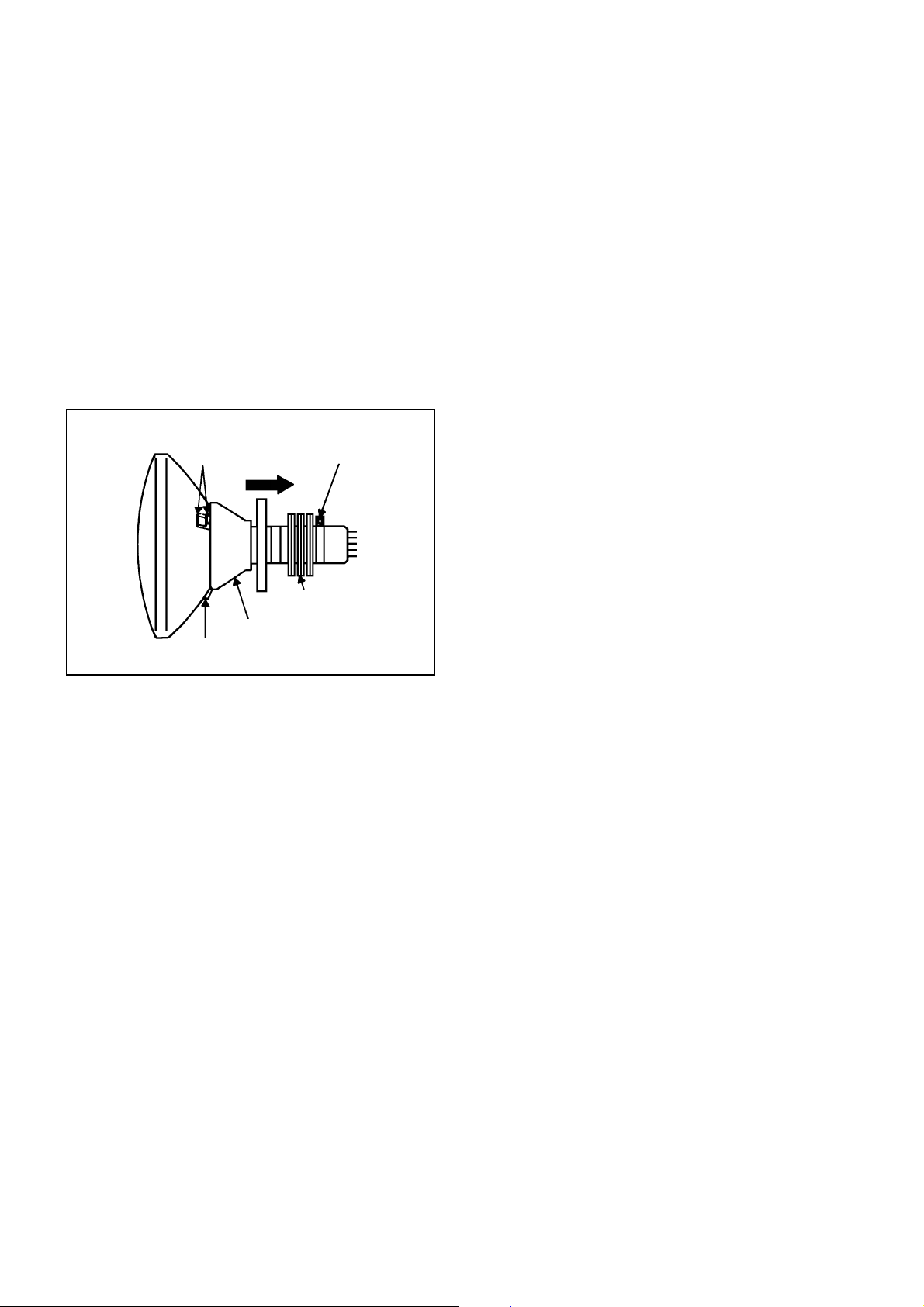
3-1: STATIC CONVERGENCE (ROUGH ADJUSTMENT)
Tighten the screw for the magnet. Refer to the adjusted
1.
CRT for the position. (Refer to Fig. 3-1)
If the deflection yoke and magnet are in one body,
untighten the screw for the body.
Receive the green raster pattern from the color bar
2.
generator.
Slide the deflection yoke until it touches the funnel
3.
side of the CRT.
Adjust center of screen to green, with red and blue on the
4.
sides, using the pair of purity magnets.
Switch the color bar generator from the green raster
5.
pattern to the crosshatch pattern.
Combine red and blue of the 3 color crosshatch pattern
6.
on the center of the screen by adjusting the pair of
4 pole magnets.
Combine red/blue (magenta) and green by adjusting the
7.
pair of 6 pole magnets.
Adjust the crosshatch pattern to change to white
8.
by repeating steps 6 and 7.
3-2: PURITY
NOTE
Adjust after performing adjustments in section 3-1.
1.
Receive the green raster pattern from color bar
generator.
2.
Adjust the pair of purity magnets to center the
color on the screen.
Adjust the pair of purity magnets so the color at the
ends are equally wide.
3.
Move the deflection yoke backward (to neck side)
slowly, and stop it at the position when the whole
screen is green.
4.
Confirm red and blue colors.
5.
Adjust the slant of the deflection yoke while watching the
screen, then tighten the fixing screw.
DEFLECTION YOKE
DEFLECTION YOKE SCREW
MAGNET SCREW
3-3: STATIC CONVERGENCE
NOTE
Adjust after performing adjustments in section 3-2.
Receive the crosshatch pattern from the color bar
1.
generator.
Combine red and blue of the 3 color crosshatch pattern
2.
on the center of the screen by adjusting the pair of
4 pole magnets.
Combine red/blue (magenta) and green by adjusting the
3.
pair of 6 pole magnets.
3-4: DYNAMIC CONVERGENCE
NOTE
Adjust after performing adjustments in section 3-3.
1.2.Adjust the differences around the screen by moving
the deflection yoke upward/downward and right/left.
(Refer to Fig. 3-2-a)
Insert three wedges between the deflection yoke and
CRT funnel to fix the deflection yoke.
(Refer to Fig. 3-2-b)
R G B
R
G
B
UPWARD/DOWNWARD SLANT RIGHT/LEFT SLANT
WEDGE
WEDGE POSITION
R
G
B
Fig. 3-2-a
WEDGE
WEDGE
Fig. 3-2-b
R G B
Fig. 3-1
PURITY MAGNETS
6 POLE MAGNETS
4 POLE MAGNETS
D2-1
Page 17

MAJOR COMPONENTS LOCATION GUIDE
TP201
L205
VR501
TP401
TU001
CP101
J801
FB401
FOCUS VOLUME
SCREEN VOLUME
MAIN
TP023
CRT
D3-1
Page 18

BLOCK DIAGRAM
ANT
TUNER
TU001
I2C 30V P.CON5V
A/V JACK
J701
OSD
V.IN1
V.IN2
V.OUT
I2C P.CON5V H.VCC
CHROMA IC
IF
V.SW IC
IC702
NJM2245L
LA76814BM-MPB
TUNER AUDIO
P.CON9V
TUNER AUDIO
IC201
P.CON9V
9V REG IC
IC601
KIA7809API
R
G
B
V.OUT
AFC
H.OUT
SOUND
12V
+5V
P.CON5V
180V
HEATER
+B
DEGAUSS
L502
R
G
B
CRT PCB
J801
EXT.SPEAKER
J702
DC JACK
J501
A.IN1
A.IN2
A.OUT
A.SW IC
IC701
NJM2234L
5V REG IC
IC103
KIA7805API
POWER CONTROL IC
IC501
FA7610CP
H.VCC
H.VCC
P.CON9V
SOUND AMP IC
IC351
AN7511
+5V
TRANS
T501
SOUND+B
SOUND
30V
+B
5V POWER REG IC
IC502
KIA7805API
30V
P.CON5V
SOUND+B
H.OUT
+B
H.OUT
Q401
FBT
FB401
V.OUT
V.OUT
IC401
LA7840
25V
V.SYNC
AFC
25V
180V
12V
HEATER
+5V
MICON
IC101
OEC3046A
DY801
CRT
V801
I2C
OSD
E-1
E-2
Page 19

PRINTED CIRCUIT BOARDS
MAIN/CRT (INSERTED PARTS)
SOLDER SIDE
OS101
W035
W008
SW108
SW107
SW106
SW101
SW102
SW103
SW104
SW105
R133
C123_1
W009
R601
R602
W010
C635
C637
W029
W030
W020
W802
C352
IC199
R139
W015
W014
C608
C613
C614
W061
IC501
W027
W023
C203
C617
C616
W846
W070
W016
R120
R136
C615
W026
R607
C204
R355
X601
C628
W053
D301
C202
IC351
C134
C625
C505_1
W012
W818
D602
C646
C627
C351
HS351
D302
C102
R212
D103
R508
Q102
C620
W814
C355
C503_1
C644
Q503
Q502
D101
Q103
CF201
TP201
W018
C354
Q101
C120
Q105
IC104
X101
C623
R117
C211
D608
D610
W832
R119
C215
D606
W065
W836
D401
D402
W013
W011
W024
R605
R506
D603
W033
C105
Q602
W034
R509
W064
W087
S100Y
C217
C606
W031
W017
L202
Q605
B504
D605
R636
R522
W077
R627
CP501
W038
C213
L205
C618
R638
Q510
W833
R611
Q508
C212
R205
C711
D607
R114_1
C636
B601
Q509
R609
W828
R610
W052
W086
R615
W066
Q601
R135
W079
C720
R604
W082
W085
W032
W048
R421
W071
R620
R407
C515
W004
VR501
L503
W092
C430
W006
W073
W080
C136_2
W078
R424
R410
W049
Q504
D504
C135
D510
C518
C514
W081
W005
R515
IC103
W058
D001
Q506
C509
C607
S100X
W051
Q507
IC502
W074
C427
W057
C417
W095
R412
R001_1
C446
W813
C001
IC601
R433
R413
C510
S101X
R404
Q402
CP401
W801
W075
R417
R415
C418
Q403
R401
C439
C440
W084
W088
C429
R423
5A125V
D508
C508
C425
R511
R446
C413
D507
Q501
C521_2
C433
C414
R411
C415
TP401
T401
Q401
W046
W063
Q505
L410
D403
W825
ICP502
IC401
W062
W830
HS001
C404
R427
W047
D503
W823
W810
W094
C512
W050
B501
D506
T501
C437
L501
L406
C513
W896
C353
W002
S801
W003
R428
CP801
C819_3
Q702
W093
D505
W042
C416
W811
C442_3
W072
W043
W069
C501
C435
W041
B502
C511_3
W831
W891
C516
W001
C443
R445
B001
W839
W019
C718
W060
C448
W076
W037
TU001
C701
C717
D702
C710
D407
C402
D404
10A125V
D509
FB401
W028
IC702
C301
D502
W059
W091
IC701
D703
W090
C403
W068
W007
W089
C434
W056
C709
D411
R806
J801
L701
W083
D705
D704
Q803
R802
W039
RY501
R804
W829
W840
R707
C712
C707
D706
D701
Q701
CP803A
W054
W067
W055
C713
CD803
C004
C703
D410
CP802B
Q801
Q802
W819
C002
CP802A
CD802
C705
L702
C715
B701
C420
R813
ICP501
C801
CP803B
R803
R805
W036
TP024 TP023
TP022
W824
CP101
J701
J702
W805
J501
W045
R429
W044
S101Y
TT
CCCCUUUUTT
R516
R422
D511
R807
VR401
R425
R426
F-1 F-2
Page 20

C719
PRINTED CIRCUIT BOARDS
MAIN/CRT (CHIP MOUNTED PARTS)
SOLDER SIDE
R518
R520
R517
R405
R409
R406
R408
R403
R130
R706
C110
C109
C106
R108
R116
R147
R146
R507
R145
1
R115
13
IC101
R118
C107
R109
R111
R501
R144
25
C506
R357
R123
C520
R504
C504
R352
C104R110
R121
R122
R124
R353
37
R502
R503
C112
C122
R505
C356
R141
C130
R106
C129
C507
R105
C519
R151
R128
R127
R101
R113
R112
R703_1
R702_1
R815_1
C805
R007
R811
C722
C804
R809
R816_1
R006
R814C806
R704
C721
R701
R709
C714
R211
R705
R710
R419R420
R414
R513
R512
R510
R514
R402
R667
R619
R614
R208
R653
R668
C226
R618
R664
C218
R203
R204
C206
R213
C216
R637
R210
C224
R623
64
C208
R206
R624
C214
C645
R622
1
C201
R606
C605
41
IC201
R612
R202
R209
C610
R613
R608
C611_1
25
R201
R131R134 R102 R103 R104
R632
C632
R661
R648
F-3
F-4
Page 21

ABC D E F GH
MICON/TUNER SCHEMATIC DIAGRAM
8
ACCESSORY
(MAIN PCB)
TU001 TECC1040PG32D
BTL
IF
9
11
10
14 15
0
0
0
NC
30.0
8
1.5
ADRES
3
NC
AGC
2
1
12 13
NC
2.0
6.9
BPL
8
7
NC
5.0
4
5
6
NC
4.8
4.8
8.8
SCL
SDA
V.S
OS101
PIC-26043LM-2
4.9
3
7
6
5
4
3
PICTURE
SW106
SKHVBED010
MENU
SW107
SKHVBED010
TV/AV
SW108
SKHVBED010
CH UP
SW101
SKHVBED010
CH DOWN
SW102
SKHVBED010
VOL UP
SW103
SKHVBED010
VOL DOWN
SW104
SKHVBED010
POWER
SW105
SKHVBED010
RESET SW
DTC114TS
TM101
R25-1213
R102
R103
R104
R101
Q105
5.6K
1.8K
1K
560
R131
R134
5.0
0
CD501
SI-PC107-67
R133
100
2206.3V KA
C123_1
1K
560
1K
R141
10K
R145
C134
D103
MTZJ5.6B
C105
C109
15P CH
47010V RS
C110
C106
18P CH
0.1 B
R112
2.2K
2.2K
R113
RESET IC
IC104 PST600C
10K
R108
VCC
GND
123
5.0 0 5.0
D101
1SS133
0
C120
0.4750V KA
V.OUT
R110
10K
100CT32R803
X101
1
C104
MICON IC
IC101
OEC3046A
R115
390K
R147
10K
0.1 B
0 0 0 0 0 5.0 4.600 0 0
0
1101112
NC
NC
0
NC
NC
0
3
X-RAY
0
VSS
1.2
56789
XT1
2.1
XT2
5.0
VDD
0
NC
2.4
AFT
5.0
KEY1
5.0
KEY2
0
NC
NC
13 14 15 16 17 18 19220 21 22 23 24
C107
2.250V KA
C102
0.033 B
150V KA
NC NC NC NC NC
NCNCNC
NC
NC
IIC BUS OFF
FILTER
CVIN
NC
-VS
-RES
2.85.0 3.1 5.0 4.30 0000 00
330
R111
1M
R109
-HS
NC
NC
POWER
R
G
B
NCNC
B.B.H
AKB DRIVE
REMOCON
BL
NC
NC
R130
0
3738394404142434445464748
AV2
EXT MUTE
TV MUTE
P.FAIL
SCL
SDA
NC
4.7K
0
AV1
0
0
NC
0
5.0
SD
5.0
NC
NC
30 31 32 33 34 35 36
0
0
NC
NC
0
NC
NC
0
5.0
25 26 27 28 29
5.0
R121 4.7K
R123 4.7K
NC
R128 10K
R127 47K
C129
47P CH
10K 1/4W
C130
47P CH
R120
4.7K 1/4W
R122
4.7K
R139
6.7
X-RAY SW
Q103
0
DTC114TS
0
C122
0.1 B
C112
0.1 B
R151
10K
3
4
4.7K
R124
VCC
0
2
GND
4.8
1
OUT
R136
12K 1/4W
R105
4.7K
R106
4.7K
1K
R146
V-BUFFER
Q101
2SC1815Y
5.0
00
0
R117
R144
D001 HZ30-3L
33K 1/4W
2.2K
W830
C001 0.022 M
R001_1
R1161KR119
H-BUFFER
4.3
2SC1815Y
0
56K 1W
Q102
W829
C002
R118
R006
27K 1/4W
10K
10006.3V YK
270
R007
5V REG. IC
IC103 KIA7805API
IN GND OUT
123
12.5 0 5.0
270
R114_1
150 1W
10035V MHE
C136_2
5678
SDA
VSS
5.005.05.0
MODE
E1
VCC
E0
1234
0000
SCL
E2
C004
C135
IC199
MEMORY IC
2
W832
4.750V KA
S100X
KA
1006.3V
S-24C01BDP
B001
BL01RN1-A63
W824
R135
22 3W
FROM/TO POWER
+5V
UNREG+12V
P.CON+5V
+B
POWER
GND
PROTECTOR
TO AV/SOUND
POWER
AV2
AV1
AUDIO_MUTE
EXT.MUTE
FROM/TO DEFLECTION/CRT
X-RAY_TEST
V_SYNC
H_SYNC
X_RAY
FROM/TO CHROMA
AGC
IF
I2C_OFF
I2C_SCL
I2C_SDA
OSD_BLANKING
OSD_BLUE
OSD_GREEN
OSD_RED
AFT_IN
7
6
5
4
3
2
1
G-1
PCB010
TM9448
NOTE:THIS SCHEMATIC DIAGRAM IS THE LATEST AT THE TIME
OF PRINTING AND SUBJECT TO CHANGE WITHOUT NOTICE
THE DC VOLTAGE AT EACH PART WAS MEASURED
NOTE:
WITH THE DIGITAL TESTER WHEN THE COLOR BROADCAST
WAS RECEIVED IN GOOD CONDITION AND PICTURE IS NORMAL.
CRITICAL FOR SAFETY,USE ONES
DESCRIBED IN PARTS LIST ONLY
ARESINCE THESE PARTS MARKED BYCAUTION:
DANGEREUSES AN POINT DE VUE SECURITE
N’UTILISER QUE CELLS DECRITES
DANS LA NOMENCLATURE DES PIECES
ETANTLES PIECES REPAREES PAR UNATTENTION:
CAUTION: DIGITAL TRANSISTOR
TUNER VIDEO SIGNAL
R.SIGNAL
G.SIGNAL
B.SIGNAL
1
DEFLECTION SIGNAL
ABC D E F GH
-
Page 22

ABC DEF GH
8
7
6
5
4
3
2
B601
0
40
0
0
2.1
0
0
1.7
1.1
0
0
0.4
30 31 32 33 34 35 36 37 38 39
2.7
5.0
2.7
0.22
2.3
2.5
NC
25 26 27 28 29
0.2250V KA
(MAIN PCB)
2216V
C615
R607
4.7K+-1%
R609
1001/4W
R608
3.9K
C618
3306.3V KA
C616 0.22TF
KA
C617
R606
R612
R605
2.7K 1/4W
C611_1
0.01B
C614
TF
C613
0.22TF
R627
120K1/4W
10K
1.8K
HOR GND
R613
1.2K
D605
150V KA
C636
HZ6B2L
4.750V KANP
R611
22K1/4W
R620
1201/2W
D607
MTZJ9.1B
D603
11E1N
1SS133
H.VCC REG
Q601
2SC2120Y
C637
0.4750V KA
R632
2.2K
D602
12
13
11.4
8.0
8.7
R615
1K1/4W
BUFFER
Q602
2SA1015Y
R604
2201/4W
R610
681/4W
W828
R638
1.2K 1/4W
560 1/4W
D606
1SS133
D608
1SS133
D610
0
R637
1SS133
1K
1016V KA
680
R653
C644
R636
2.0
0
14
9V REG IC
IC601
KIA7809API
GNDIN OUT
123
11.5 0 8.9
C607
47010V YK
CHROMA SCHEMATIC DIAGRAM
R668
0
2.4K
R667
150V KA
C606
2.2K
AFT
R601 1K 1/4W
W833
W814
R618 2.2M
C620 2.250V KA
BUS
1211
R602 1K 1/4W
10
9
C646
2.42.2
2.2
CLMPCLMP
VIDEO
SW
TRAP
DELAY
LINE
PEAKING
CORING
BLACK
STRETCH
DC
RES
OSD
FIX GAIN
ABL
CLAMP
13
R648 10K
R619
1K
1K
R614
VCO
C216
L205
3602038
1
6
2
34
FROM/TO AV/SOUND
P.CON+9V
SWD_VIDEO
DIVERSITY
TUNER_VIDEO
SWD_AUDIO
AUDIO_OUT
TU_AUDIO_OUT
C211
R204
1K
R213
10K
L202
0.47uH
R211
68
FROM/TO MICON/TUNER
IF X_RAY
AGC H_SYNC
AFT_IN H_OUT
I2C_SDA V_OUT
I2C_SCL FBT+12V
OSD_RED ABCL
OSD_GREEN CLAMP
OSD_BLUE B.OUT
OSD_BLANKING G.OUT
I2C_OFF R.OUT
R210
12345
150V KA
47K
R208
220
C206
5
C208
OUTOUTGININ
C218
0.001 B
C217
R203
B
1K
0.001
R205
1001/4W
C212 0.018 TF
C213 0.022 TF
B
0.01
SAW FILTER
CF201
M1958M
R206
2.2K
C224
5PCH
0.4750V KA
7
C226
R212
22PCH
5.6K 1/4W
C214
3.0
6566676869
2.2
2.0
2.5
3.0
0
70717273747576777879
0
0
2.8
0
2.4
0
1.5
0
2.9
0
0.01 B
CHR0MA IC
LA76814BM-MPB
3P CH
NC
0 0 4.1 4.1 000003.3
0
NC NC NC NC
50
51
52
53
54
NC
NC
NC
1
NC
2
3
4
5
6
7
NC NC NC NC NC NC
NC
3
1 101112131415161718192 20 21 22 23 24
00 00 0 0000 0000
IC201
C202
2206.3V KA
8
150V KA
C215
TP201
0.30
0 5.0 1.73.30.32.72.6
49 48 47 46 45 44 43 42 41 40 39 38 37 36
A2C
PLL
VIDEO
TRAP
RF AGC
NC
4
AMP
SPLL
BPF BPF
SW
DC
VOL
IF AGC
C201
0.01
B
W818
C204
W819
LIM
AMP
FM
DET
R209
7
R202
R201
0.1TF
100K
100K
C203
150V KA
7.5K
VIF
8809
VIDEO
DET
1098
VIDEO
BUFFER
0.3
2SA1015Y
5.0
470
R664
150V KA
V/C GND
NC
BPF
SW
ACC
DEMO
COLOR
CLAMP
CONTRAST RGB
BRIGHT
Q605
C632
1016V KA
C625
NC
APC1
SYNC
SEP
MATRIX
OSD
SW
DRIVE/CUT-OFF
27P CH
X601
100CT3R505
R622
C605 0.01 B
C645 15P CH
11
CW
VC0
KIL X-RAY
FILTER
TINT
HOR
VCO
1/256
HOR
C/D
AFC1
VER
SEP
VER
C/D
2120191817161514
2.62.6
15
16
1K
C627
R623
ADJ
04.8 2.5 2.4 0 4.6 3.9 7.8 2.6
17
C623
24K
0.4750V KA
FBP
AFC2
PHASE
SHIFTER
HOR
OUT
HOR
VOC
VER
RAMP
AKB
C608
10006.3V RZ
R624
24K
C6280.047TF
C610100PCH
NCNC NC
4716V KA
R661
56K
0
41424344454647484955051525354555657585966061626364
NC
CLK
REF
H_GND
NC
BL02RN1-R62
35
34
33
32
31
30
29
28
NC
27
26
25
24
23
22
C635
FROM POWER
UNREG+12V
GND
P.CON+5V
FROM/TO DEFLECTION/CRT
8
7
6
5
4
3
2
1
G-3
THE RESISTOR MARKED F IS FUSE RESISTOR.NOTE:
THE ALUMI ELECTROLYTIC CAPACITOR MARKED NP
IS NON POLAR ONE.
NOTE:THIS SCHEMATIC DIAGRAM IS THE LATEST AT THE TIME
OF PRINTING AND SUBJECT TO CHANGE WITHOUT NOTICE
CP101
GND
TEST POINT
I2C_SCL
8283_0612_00_000
6
THE DC VOLTAGE AT EACH PART WAS MEASURED
NOTE:
WITH THE DIGITAL TESTER WHEN THE COLOR BROADCAST
WAS RECEIVED IN GOOD CONDITION AND PICTURE IS NORMAL.
I2C_SDA
I2C_OFF
B.OUT
R.OUT/AGC
12345
CRITICAL FOR SAFETY,USE ONES
DESCRIBED IN PARTS LIST ONLY
ARESINCE THESE PARTS MARKED BYCAUTION:
DANGEREUSES AN POINT DE VUE SECURITE
N’UTILISER QUE CELLS DECRITES
DANS LA NOMENCLATURE DES PIECES
ETANTLES PIECES REPAREES PAR UNATTENTION:
TUNER VIDEO SIGNAL
R.SIGNAL
G.SIGNAL
B.SIGNAL
DEFLECTION SIGNAL
AUDIO SIGNAL
LUMINANCE SIGNAL
COLOR SIGNAL
PCB010
TM9448
1
ABC DEF GH
G-4
Page 23

8
FROM CHROMA
7
6
FROM/TO MICON/TUNER
5
FROM/TO CHROMA
4
3
2
1
ABC DEF GH
CP801
TBS-X01X-A1
FOCUS
SCREEN
HEATER
GND
GND
+B
(MAIN PCB)
5
GND
4
CLAMP
3
G.OUT
2
B.OUTB.OUT
R.OUT
1
CP802B
51048-0510
1
S801
0.0012KV YR
C819_2
4
3
2
1
CP803B
51052-0400
PCB110
TC9306
C804
330P B
R809
3.2
2.7128.0
RED OUT
Q801
2SC3415
R813
TP022 TP024
1/4W
2W
R802
R803
15K
2.7K
96.4
6.4
3
4
0
5
0
6
7
101.6
8
9
99.6
J801
HPS3200-010501
220
126.0 2.7
GREEN OUT
Q802
2SC3415
4.7K 1/4W
2W
R805
15K
0
1
F
R804
C805
R815_1
25 2624
2.7K 1/4W
330P B
R811
4.7K
TP023
220
3.23.2
120.5 2.7
BLUE OUT
2SC3415
2W
R807
15K
Q803
R806
C806
R816_1
1/4W
2.7K
470P B
4.7K
R814
220
C801
8
7
6
5
100P B
4
3
2
CLAMP
G.OUT
B.OUT
R.OUT
FROM POWER
P.CON+5V_A
V_SYNC
X-RAY_TEST
H_SYNC
X_RAY
V_OUT
X_RAY
ABCL
H_OUT
H_SYNC
FBT+12V
FROM POWER
180V
+B
GND
W850
(W052)
R401
100K1/4W
+-1%
C439
SL
22P500V
27.0
0.3
C416
100V PP
0.0047
TP401
R412
6.8K7W
0
L406
68uH
D401
19
18
H.DRIVE
Q402
2SC2271
R428
6.8
R404
1.8K1/4W
D402
HZ27-1L
HZ11B1L
R446
C440
1/2W
R414
3.3K
1/2W
4.7K
B
560P500V
R405
27K +-1%
T401
305Y002
34
2
NC
1
C446
6
20
C404
1250V MHE
DEFLECTION/CRT SCHEMATIC DIAGRAM
W840
V-OUT IC
IC401 LA7840
THERMAL
PROTECTION
-
AMP
MHE
0909
ECWH
C415
500V
C429
0.0056B
W810
C437
W823
W896
C442_3
+
82P
ECWF
0.22250V
470P2KV R
SL
R415
160V MHE
GND
1234567
R402
18K
R406
19.4
12K +-1%
R408
1.5K
15K+-1%
H.OUTPUT
Q401
2SD2599
(LBOEC1)
680P500V B
R427
0 12.6 25.8 2.6 2.6 25.3 2.2
18K
4.750V MHE
R403
C425
X-RAY TEST SW
Q403
DTA114ES
19.59.2
R409
2.2250V
C413
R423
68 1/2W
L410
C403
W891
0
27K1/4W
AU02A-EIC
47016V MHE
4.7mH
0.00271.6KV
C443
W831 W811
R422
C402
470P500V B
D404
21
130.0
0
100 1/4W
R417
10K
+-1%
11K +-1%
W813
D410
AU02A-EIC
C420
0.0011KV
C448
22
VCC
R407
B
R419
C417
PUMP
UP
C414
1.8K
1.5 1W
2.250V MHE
130.0
137.0
10035V
R420
24K
0.6
MHE
C418
COL
1
VIDEO
6
B+
2
0
AFC
9
HEA
0
TER
10
0
GND
8
0
E12
4
0
E25
3
22
R410
1000
25V MHE
C427
FB401 3210011F
R445
270K
1/4W
180 3W
ABL
GND
D403
11E1N
S101X
1050V MHE
R429
4.7
GND
E8
C430
GND
R413
1W
HV
F
S
0
11
0.3
7
0
8
0
5
NC
AU02A-EIC
C435
0.1100V TF
1.5K1/2W
1/2W
1.2K
D407
TF
0.1
100V
GND GND
CLAMP CLAMP
G.OUT G.OUT
B.OUT B.OUT
R.OUT R.OUT
51048-0510
R424
R411
270
270
1/2W
1/2W
S101Y
23
GND
V.POSI.
R433
C434
D411
AU02A-EIC
C433
100035V MHE
R421
68K 1/4W
5
GND
4
CLAMP
3
G.OUT
2
1
R.OUT
CP802A
1K
METAL
VR401
R425
270 1/2W
R426
270 1/2W
4
22100V MHE
3
2
1
CP401
B04B-DVS
HEATER HEATER
4
GND GND
3
GND GND
2
+B +B
1
CP803A
51052-0400
PCB010
TM9448
K001
TMM17538
K002
TMM17538
K003
TMM17538
V801
A22JQG098X
4
5
7
9
3
DY801
KDY3CFB23M
4
3
2
1
CD802
6814038
R
G
B
CD803
2E041703
186
R.SIGNAL
CAUTION: DIGITAL TRANSISTOR
THE DC VOLTAGE AT EACH PART WAS MEASURED
NOTE:
WITH THE DIGITAL TESTER WHEN THE COLOR BROADCAST
WAS RECEIVED IN GOOD CONDITION AND PICTURE IS NORMAL.
CRITICAL FOR SAFETY,USE ONES
DESCRIBED IN PARTS LIST ONLY
ARESINCE THESE PARTS MARKED BYCAUTION:
DANGEREUSES AN POINT DE VUE SECURITE
N’UTILISER QUE CELLS DECRITES
DANS LA NOMENCLATURE DES PIECES
ETANTLES PIECES REPAREES PAR UNATTENTION:
THE RESISTOR MARKED F IS FUSE RESISTOR.NOTE:
THE ALUMI ELECTROLYTIC CAPACITOR MARKED NP
IS NON POLAR ONE.
NOTE:THIS SCHEMATIC DIAGRAM IS THE LATEST AT THE TIME
OF PRINTING AND SUBJECT TO CHANGE WITHOUT NOTICE
G.SIGNAL
B.SIGNAL
DEFLECTION SIGNAL
1
ABC DEF GH
G-6G-5
Page 24

ABC D E F GH
POWER SCHEMATIC DIAGRAM
8
DC JACK
7
J501
HEC0824-010010
2
3
1
10A 125V
ICP501
251010
D502
L501
11E1N
10uH
D511
1SS133
RY501
ALKS329
3
4
POWER FAIL
Q501
DTC114ES
12
0.9
0
0
D503
1SS133
DC POWER SW.
2SC2120Y
Q504
0
0
0
R510
DC POWEWR SW
Q509
DTA114ES
R514
11.5
3.3K
3.3K
11.5
D504
MTZJ16B
0
DC POWER SW
Q510
DTC114ES
R512
1K
0
4.8
0
6
100025V ZL
C516
1016V KA
C503_1
C520
5
470P B
4
W836
100025V ZL
C501
R501
180K
R502
330K
R503
68K
2.6 0.9 14.4
VREF
BIAS
U.V.LO
0.52V
+
-
ER.
POWER CONTROL IC
AMP.
IC501 FA7610CP
1234
0.5 0
C504
0.0033
R504
C506
R505
C505_1
820P B
0.4
1.5V
30uA
OSC
+
-
+
S.C.P
OFF
+
+
-
OFF
PWM
1.0 5.3
B
12K
0.1 B
390
B504
5678
LO
500OHM
REG DRIVER
C519
BL01RN1-A63
5.3
Q502
2SC1740STP
5.3
R507
0.001 B
1K
C507
R508
14.1
0.01 B
100 1/4W
5.4
5.3
REG DRIVER
0
R509
2.2 1/4W
Q503
2SA952_L
763WAA0134
POWER REG
2SK2903-01MR
5.3
HS001
T501 8128019W
12.0
7
D505
8
HZ27-1L
12.0
D506
B501
BL02RN1-R62
Q505
20.0
D
G
0
S
0.01100V TF
C508
AU02A-EIC
11.9
11.9
11
12
(TV MAIN PCB)
PROTECTOR
Q506
DTC114ES
0
2.2K
C509
R513
0.068 M
-10.7
1
0
2
0
3
0
4
0
5
0
6
4.1
0
B502
BL02RN1-R62
5A 125V
ICP502
251005
D507
21DQ09N
C521_2
220P2KV R
DEGAUSS COIL
8R090007
C510
470P500V B
D508
21DQ09N
R515
0.47 3W
L502
C511_3
220P2KV R
D509
RU2AM
C514
C512
8
R518
3.3K
2.7K
R517
0 0.5
CP501
TV-50P-02-L1
21
2
1
C513
100160V PR
47016V
MHE
R522
47010V
MHE
3.3 1W
R516
C515
4.7250V ECQ-E
S100Y
180K 1/2W
C
G
Q507
CR2AM-8-F8
A
0.6
D510
AU02A-EIC
W839
5V POWER REG IC
IC502
KIA7805API
0.5
5.0
DEGAUSS SW
Q508
DTA114ES
5.0
R520
1K
FROM/TO MICON/TUNER
+5V
UNREG+12V
PROTECTOR
POWER
GND
+B
P.CON+5V
FROM/TO DEFLECTION/CRT
180V
+B
P.CON+5V_A
GND
TO CHROMA
UNREG+12V
P.CON+5V
GND
TO AV/SOUND
SOUND+B
P.CON+5V_A
GND
(SOUND)
GND
P.CON+5V
7
6
5
4
3
2
10A 125V
CAUTION:
FOR CONTINUED PROTECTION AGAINST FIRE HAZARD,
REPLACE ONLY WITH THE SAME TYPE FUSE
1
10A 125V (ICP501) , 5A 125V (ICP502).
ATTENTION: POUR UNE PROTECTION CONTINUE LES RISQUES D’INCEIE
N’UTILISER QUE DES FUSIBLE DE MEME TYPE
10A 125V (ICP501) , 5A 125V (ICP502).
5A 125V
ABC D E F GH
+B ADJ.
R506
3.3K 1/4W
THE DC VOLTAGE AT EACH PART WAS MEASURED
NOTE:
WITH THE DIGITAL TESTER WHEN THE COLOR BROADCAST
WAS RECEIVED IN GOOD CONDITION AND PICTURE IS NORMAL.
VR501
METAL
10K
R511
68K 1/4W
NOTE:THIS SCHEMATIC DIAGRAM IS THE LATEST AT THE TIME
OF PRINTING AND SUBJECT TO CHANGE WITHOUT NOTICE
CRITICAL FOR SAFETY,USE ONES
DESCRIBED IN PARTS LIST ONLY
W801
GND OUTIN
123
8.3 0 5.0
W851
(W074)
C518
L503
10uH 0607
10006.3V YK
3
2
PCB010
CAUTION: DIGITAL TRANSISTOR
ARESINCE THESE PARTS MARKED BYCAUTION:
DANGEREUSES AN POINT DE VUE SECURITE
N’UTILISER QUE CELLS DECRITES
DANS LA NOMENCLATURE DES PIECES
ETANTLES PIECES REPAREES PAR UNATTENTION:
CAUTION: DIGITAL TRANSISTOR
TM9448
1
G-8G-7
Page 25

ABC D E F GH
AV/SOUND SCHEMATIC DIAGRAM
8
FROM MICON/TUNER
AUDIO_MUTE
POWER
R353
68K
47K 1/4W
7
FROM/TO CHROMA
AUDIO_OUT
6
P.CON+9V
TU_AUDIO_OUT
SWD_AUDIO
TUNER_VIDEO
SWD_VIDEO
C355
1016V KA
(TV MAIN PCB)
R355
W846
R352
8
7
D302
MTZJ12B
2.04.5 0 2.0
5678
+-
0003.8
1234
D301
MTZJ12B
IC351
AN7511
SOUND AMP IC
C353
47016V YK
W802
C301
47016V YK
W805
EXT.SPEAKER/DIVERSITY
C719
0.001 B
J702
TC38-001-05-T
2
3
NC
1
6
10K
C356
47010V RS
R357
C354
0.033 B
100K
C351
150V KA
C352
4716V KA
HS351
763WSA0009
NC
5
D704 MTZJ12B
C722
C712
0.001 B
1.9
IC702 NJM2245LVIDEO SW IC
LH
1016V KA
R707
100 1/4W
2SA1015Y
0
C713
D705 MTZJ12B
BUFFER
Q701
2.5
BUFFER
BIAS
1016V KA
C714
0.01 B
C718
R709
3.3K
1K
R710
L701
100uH
FROM POWER
10016V YK
C709
B701
BL01RN1-A63
4716V KA
L702
100uH
1006.3V KA
C715
C721
0.022 B
(SOUND)
SOUND+B
GND
P.CON+5V
GND
PCB010
TM9448
IC701 NJM2234LAUDIO SW IC
LH
LH
12345678
5.2 0.1 5.3 0.1 3.9 8.6 04.6
4
3
2
FROM MICON/TUNER
EXT.MUTE
A_OUT
A_IN_1
A_IN_2
V_OUT
V_IN_1
V_IN_2
AV1
AV2
J701
YKC21-7223
E
1
E
5
R706
2.2K
234
H3 H2 H1
678
H3 H2 H1
R702_175R703_1
C717
4.750V KA
C720
75
150V KA
C701
1050V YK
0
0
0.4
D702 MTZJ12B
MUTE SW
Q702
2SC1815Y
C703
150V KA
C705
D703 MTZJ12B
BUFFER
BIAS
150V KA
R704
W825
75
1K
R705
R701
C707
C711
1016V KA
1K
1016V KA
D706
MTZJ12B
LH
12345678
5.7 0.2 5.8 0.2 5.8 9.3 5.0 0
C710
4706.3V YK
D701
MTZJ6.8B
5
4
3
2
1
THE DC VOLTAGE AT EACH PART WAS MEASURED
NOTE:
WITH THE DIGITAL TESTER WHEN THE COLOR BROADCAST
WAS RECEIVED IN GOOD CONDITION AND PICTURE IS NORMAL.
NOTE:THIS SCHEMATIC DIAGRAM IS THE LATEST AT THE TIME
OF PRINTING AND SUBJECT TO CHANGE WITHOUT NOTICE
CRITICAL FOR SAFETY,USE ONES
DESCRIBED IN PARTS LIST ONLY
ARESINCE THESE PARTS MARKED BYCAUTION:
DANGEREUSES AN POINT DE VUE SECURITE
N’UTILISER QUE CELLS DECRITES
DANS LA NOMENCLATURE DES PIECES
ETANTLES PIECES REPAREES PAR UNATTENTION:
AUDIO SIGNAL
TUNER VIDEO SIGNAL
1
ABC D E F GH
G-10G-9
Page 26

MICON/TUNER
WAVEFORMS
10.5V 10µs/div
31.0V 20µs/div
41.0V 5ms/div
80.5V 10µs/div
90.5V 10µs/div
10200mV 10µs/div
13200mV 20µs/div
14200mV 5ms/div
150.5V 20µs/div
CHROMA
520.0mV 1ms/div
11100mV 0.1µs/div
The following waveforms were measured at the point of the corresponding
NOTE:
balloon number in the schematic diagram.
160.5V 20µs/div
170.5V 20µs/div1210.0V 20µs/div 7200mV 50µs/div
H-1
Page 27

DEFLECTION/CRT
WAVEFORMS
18200mV 5ms/div
1920.0V 20µs/div
205.0V 20µs/div
2310.0V 5ms/div
2410.0V 20µs/div
2510.0V 20µs/div
21200V 20µs/div
225.0V 5ms/div
2610.0V 20µs/div
The following waveforms were measured at the point of the corresponding
NOTE:
balloon number in the schematic diagram.
H-2
Page 28

MECHANICAL EXPLODED VIEW
109
205
110 205
205
L502
J801
PCB110
(CRT PCB)
201
201
107
108
201
202
201
FB401
J701
V801
103
204
205
204
TU001
102
PCB010
(MAIN PCB)
203
104
106
105
101
I-1
Page 29

MECHANICAL REPLACEMENT PARTS LIST
REF. NO. PART NO. DESCRIPTION
101 A3I506I720 CABINET,FRONT ASS'Y
102 735WPAA423 REMOCON HOLDER
103 701WPJB504 CABINET,FRONT
104 713WPA0101 GUIDE,REMOCON
105 735WPAA402 BUTTON,FRAME
106 735WPAA403 BUTTON,HOLDER
107 702WPA0666 CABINET,BACK(1/4)
108 722A08A096 SHEET,RATING
109 7260000321 SHEET,CRT SERVICEMAN
110 741WUA0019 SPRING,EARTH
201 8117540A64 SCREW,TAPPING(B0) TRUSS 4x16
202 8110630A04 SCREW,TAP TITE(P) BRAZIER 3x10
203 8110630804 SCREW,TAP TITE(P) BRAZIER 3x8
204 8109I30A04 SCREW,TAP TITE(B) WH7 3x10
205 8141J40B84 SCREW,TAP TITE(P) GW1 4x28
JA5K0100 POLY BAG
J3I50601 INSTRUCTION BOOK
--- A3I506I975 INSTRUCTION BOOK KIT
--- 792WHA0256 PACKAGE,BOTTOM
--- 792WHA0255 PACKAGE,TOP
--- 791WHA0022 LAMIFILM BAG
793WCDB102 GIFT BOX
J1-1
Page 30

ELECTRICAL REPLACEMENT PARTS LIST
REF. NO. PART NO. DESCRIPTION REF. NO. PART NO. DESCRIPTION
RESISTORS DIODES
! R001 R3X181563J R,METAL OXIDE 56K OHM 1W or D610 D1VT001330 DIODE,SILICON 1SS133T-77
R114 R3X101151J R,METAL 150 OHM 1W D702 D97U01201B DIODE,ZENER MTZJ12B T-77
! R135 R3X28B220J R.METAL 22 OHM 3W D703 D97U01201B DIODE,ZENER MTZJ12B T-77
! R401 R4X5T4104F R,METAL 100K OHM 1/4W D704 D97U01201B DIODE,ZENER MTZJ12B T-77
! R404 R002T4182J RC 1.8K OHM 1/4W D705 D97U01201B DIODE,ZENER MTZJ12B T-77
! R405 R801R7273F RC 27K OHM 1/10W D706 D97U01201B DIODE,ZENER MTZJ12B T-77
! R406 R801R7123F RC 12K OHM 1/10W
! R407 R3X2811R5J R.METAL OXIDE 1.5 OHM 1W IC101 I53F03046A IC OEC3046A
! R408 R801R7152J RC 1.5K OHM 1/10W ! IC103 I1KA97805A IC KIA7805API
! R409 R801R7153F RC 15K OHM 1/10W IC104 I9UJ0T600C IC PST600C
R410 R3X28B181J R.METAL 180 OHM 3W IC199 A3I501I015 IC S-24C01BDP
! R412 R5X2CE682J R,CEMENT 6.8K OHM 7W IC201 I03FE814B0 IC LA76814BM-MPB
R423 R65582680J R,FUSE 68 OHM 1/2W ! IC351 I01DP75110 IC AN7511
R429 R655814R7J R,FUSE 4.7 OHM 1W ! IC401 I03SD78400 IC LA7840
! R509 R002T42R2J RC 2.2 OHM 1/4W ! IC501 IDJD076100 IC FA7610CP
R515 R3X28BR47J R.METAL OXIDE 0.47 OHM 3W ! IC502 I1KA97805A IC KIA7805API
! R522 R3X1813R3J R,METAL OXIDE 3.3 OHM 1W IC601 I1KA97809A IC KIA7809API
! R606 R801R7103J RC 10K OHM 1/10W IC701 I0QS02234L IC NJM2234L
! R803 R3X28A153J R,METAL OXIDE 15K OHM 2W IC702 I0QS02245L IC NJM2245L
! R805 R3X28A153J R,METAL OXIDE 15K OHM 2W
! R807 R3X28A153J R,METAL OXIDE 15K OHM 2W Q101 TC5T018154 TRANSISTOR,SILICON 2SC1815Y(TPE2)
! C403 E5EZT2471M CE 470 UF 16V Q103 TNYTJ03001 COMPOUND TRANSISTOR DTC114TSTP
! C414 E5EZT4101M CE 100 UF 35V Q105 TNYTJ03001 COMPOUND TRANSISTOR DTC114TSTP
! C418 E5EZF3102M CE 1000 UF 25V or ! Q401 TDUU025990 TRANSISTOR SILICON 2SD2599(LBOEC1)
! C433 E5EZF4102M CE 1000 UF 35V Q403 TPYTB03001 COMPOUND TRANSISTOR DTA114ESTP
! C434 E5EZT8220M CE 22 UF 100V Q501 TNYTB03001 COMPOUND TRANSISTOR DTC114ESTP
C437 P411F3224J CMPP 0.22 UF 250V ECWF or Q502 TCYT1740S0 TRANSISTOR,SILICON 2SC1740STP
C442 C03L0R7Q2K CC 470 PF 2KV R Q504 TC5T021204 TRANSISTOR,SILICON 2SC2120Y(TPE2)
! C443 P414F9272H CMPP 0.0027UF 1.6KV ECWH or ! Q505 T410029030 FET 2SK2903-01MR
! C446 E5EZTD010M CE 1 UF 250V ! Q507 TF6FR2AM80 THYRISTOR CR2AM-8-F8
! C448 E5EZTB220M CE 22 UF 160V Q508 TPYTB03001 COMPOUND TRANSISTOR DTA114ESTP
C501 E62FF3102M CE 1000 UF 25V Q509 TPYTB03001 COMPOUND TRANSISTOR DTA114ESTP
C511 C03L0R7H2K CC 220 PF 2KV R Q510 TNYTB03001 COMPOUND TRANSISTOR DTC114ESTP
! C512 E5EZT2471M CE 470 UF 16V Q601 TC5T021204 TRANSISTOR,SILICON 2SC2120Y(TPE2)
! C513 E53VFB101M CE 100 UF 160V Q602 TA5T010154 TRANSISTOR,SILICON 2SA1015Y(TPE2)
! C514 E5EZT1471M CE 470 UF 10V Q605 TA5T010154 TRANSISTOR,SILICON 2SA1015Y(TPE2)
C515 P21503475K CMP 4.7 UF 250V ECQ-E Q701 TA5T010154 TRANSISTOR,SILICON 2SA1015Y(TPE2)
C516 E62FF3102M CE 1000 UF 25V Q702 TC5T018154 TRANSISTOR,SILICON 2SC1815Y(TPE2)
! C518 E02LT0102M CE 1000 UF 6.3V ! Q801 TCYT034150 TRANSISTOR,SILICON 2SC3415T93-(N,P)
C521 C03L0R7H2K CC 220 PF 2KV R ! Q802 TCYT034150 TRANSISTOR,SILICON 2SC3415T93-(N,P)
! C615 E50HU2220M CE 22 UF 16 V ! Q803 TCYT034150 TRANSISTOR,SILICON 2SC3415T93-(N,P)
C819 C0JLYR713K CC 0.001 UF 2KV YR or
D001 D94TA30013 DIODE ZENER HZ30-3L TD L406 021U6D680K COIL 68 UH
D101 D1VT001330 DIODE,SILICON 1SS133T-77 L410 021679472K COIL 4.7 MH
D103 D97U05R61B DIODE,ZENER MTZJ5.6B T-77 L501 021W67100M COIL 10 UH
D301 D97U01201B DIODE,ZENER MTZJ12B T-77 ! L502 028R090007 COIL,DEGAUSS 8R090007
D302 D97U01201B DIODE,ZENER MTZJ12B T-77 L503 02167D100K COIL 10 UH
! D401 D94TA27011 DIODE ZENER HZ27-1L TD L701 021673101K COIL 100 UH
! D402 D94TA11B11 DIODE ZENER HZ11B1L TD L702 021673101K COIL 100 UH
D403 D28T11E1N1 DIODE SILICON 11E1N-TA1B2 T401 03305Y002S TRANS,HORIZONTAL DRIVE 305Y002
! D404 D2WTAU02A0 DIODE SILICON AU02A-EIC ! T501 048128019W TRANSFORMER,SWITCHING 8128019W
! D407 D2WTAU02A0 DIODE SILICON AU02A-EIC
! D410 D2WTAU02A0 DIODE SILICON AU02A-EIC ! J501 0602602006 JACK DC HEC0824-010010
! D411 D2WTAU02A0 DIODE SILICON AU02A-EIC J701 060Q441002 RCA JACK YKC21-7223
D502 D28T11E1N1 DIODE SILICON 11E1N-TA1B2 ! J702 060C121010 EAR PHONE JACK 3.5 TC38-001-05-T
D503 D1VT001330 DIODE,SILICON 1SS133T-77 ! J801 066X120014 SOCKET,CRT HPS3200-010501
D504 D97U01601B DIODE ZENER MTZJ16B T-77
! D505 D94TA27011 DIODE ZENER HZ27-1L TD SW101 0504201T31 SWITCH,TACT SKHVBED010
! D506 D2WTAU02A0 DIODE SILICON AU02A-EIC SW102 0504201T31 SWITCH,TACT SKHVBED010
! D507 D28T21DQN9 DIODE SCHOTTKY 21DQ09N-TA2B1 SW103 0504201T31 SWITCH,TACT SKHVBED010
! D508 D28T21DQN9 DIODE SCHOTTKY 21DQ09N-TA2B1 SW104 0504201T31 SWITCH,TACT SKHVBED010
! D509 D2BTRU2AM0 DIODE SILICON RU2AM V1 SW105 0504201T31 SWITCH,TACT SKHVBED010
D510 D2WTAU02A0 DIODE SILICON AU02A-EIC SW106 0504201T31 SWITCH,TACT SKHVBED010
D511 D1VT001330 DIODE,SILICON 1SS133T-77 SW107 0504201T31 SWITCH,TACT SKHVBED010
D602 D1VT001330 DIODE,SILICON 1SS133T-77 SW108 0504201T31 SWITCH,TACT SKHVBED010
D603 D28T11E1N1 DIODE SILICON 11E1N-TA1B2
D605 D94TA6RB12 DIODE ZENER HZ6B2L TD VR401 V126213BT2 VOLUME,SEMI FIXED RH0684C13R
D606 D1VT001330 DIODE,SILICON 1SS133T-77 VR501 V126214BT2 VOLUME,SEMI FIXED RH0684C14R
D607 D97U09R11B DIODE,ZENER MTZJ9.1B T-77
D608 D1VT001330 DIODE,SILICON 1SS133T-77 PCB010 A3I506I010 PCB ASS'Y TM9448A
R3U28A563J R,METAL OXIDE 56K OHM 2W D701 D97U06R81B DIODE,ZENER MTZJ6.8B T-77
ICS
TRANSISTORS
CAPACITORS
E02YF3102M CE 1000 UF 25V ! Q402 TC3T022710 TRANSISTOR,SILICON 2SC2271(D,E)-AE
P447F2224J CMPP 0.22 UF 200V FHS ! Q503 TAST00952L TRANSISTOR,SILICON 2SA952(C)-T_L
P4J239272H CMPP 0.0027UF 1.6KV Q506 TNYTB03001 COMPOUND TRANSISTOR DTC114ESTP
Q102 TC5T018154 TRANSISTOR,SILICON 2SC1815Y(TPE2)
COILS &TRANSFORMERS
C01BBP713K CC 0.001 UF 2KV BP L202 021673R47M COIL 0.47 UH
DIODES
L205 0336020388 COIL VIDEO IFT 3602038
JACKS
SWITCHES
VARIABLE RESISTORS
P.C.BOARD ASSEMBLIES
J2-1
Page 31

ELECTRICAL REPLACEMENT PARTS LIST
REF. NO. PART NO. DESCRIPTION
P.C.BOARD ASSEMBLIES
PCB110 A3I506I110 PCB ASS'Y TC9306A
MISCELLANEOUS
B001 024AT03655 CORE BEADS BL01RN1-A63T6
B501 024AT03481 CORE,BEADS BL02RN1-R62T2
B502 024AT03481 CORE,BEADS BL02RN1-R62T2
B504 024AT03655 CORE BEADS BL01RN1-A63T6
B601 024AT03481 CORE,BEADS BL02RN1-R62T2
B701 024AT03655 CORE BEADS BL01RN1-A63T6
CD501 121B164101 CORD,CAR BATTERY SI-PC107-67
CD802 WCL6814038 FLAT CABLE AWG26 5C GRAY 140MM
CD803 WBL6018038 FLAT CABLE AWG26 4C BLACK 180MM
CF201 102E245R71 FILTER,SAW M1958M
CP101 069E260129 CONNECTOR PCB SIDE 8283_0612_00_000
CP401 069X440029 CONNECTOR PCB SIDE B04B-DVS
CP501 069W420069 CONNECTOR PCB SIDE TV-50P-02-L1
CP801 069W010030 CONNECTOR PCB SIDE TBS-X01X-A1
CP802A 067R005019 WIRE HOLDER 51048-0510
CP802B 067R005019 WIRE HOLDER 51048-0510
CP803A 067R104019 WIRE HOLDER 51052-0400
CP803B 067R104019 WIRE HOLDER 51052-0400
CUS001 800WFAA006 CUSHION A
! DY801 0271080901 DY KDY3CFB23M
! FB401 043210011F TRANSFORMER,FLYBACK 3210011F
! ICP501 083PC10002 MICRO FUSE 251010
! ICP502 083PC05002 MICRO FUSE 251005
K001 1291000016 WEDGE TMM17538
K002 1291000016 WEDGE TMM17538
K003 1291000016 WEDGE TMM17538
OS101 077Q014005 REMOTE RECEIVER PIC-26043LM-2
RY501 0560V50118 RELAY ALKS329
TM101 076R0CX010 TRANSMITTER R25-1213
! TU001 0145K00055 TUNER,VHF-UHF TECC1040PG32D
! V801 09D1090401 CRT W/O DY A22JQG098X
X101 100C32R803 CRYSTAL DSVT-200 32.768KHz
X601 100CT3R505 CRYSTAL HC-49/C 3.579545MHz
RESISTOR
RC................... CARBON RESISTOR
CAPACITORS
CC................... CERAMIC CAPACITOR
CE................... ALUMI ELECTROLYTIC CAPACITOR
CP................... POLYESTER CAPACITOR
CPP..................POLYPROPYLENE CAPACITOR
CPL.................. PLASTIC CAPACITOR
CMP................. METAL POLYESTER CAPACITOR
CMPL............... METAL PLASTIC CAPACITOR
CMPP...............METAL POLYPROPYLENE CAPACITOR
J2-2
Page 32

SPEC.NO.
M3I5-06I
O/R NO.
WIX3011
 Loading...