

Page 1

Virtex-4™ MB Development Board
User’s Guide
Version 3.0
December 2005
Page 2
i
Table of Contents
1 OVERVIEW .....................................................................................................................1
2 THE VIRTEX -4 MB SYSTEM BOARD ..............................................................................1
3 FUNCTIONAL DESCRIPTION .........................................................................................2
3.1 LVDS INTERFACE .......................................................................................................3
3.1.1 SPI-4.2 Interface.................................................................................................4
3.1.2 SPI-4.2 Pin Assignments .....................................................................................4
3.1.3 LVDS Connector .................................................................................................6
3.2 DDR SDRAM ............................................................................................................7
3.3 FLASH.......................................................................................................................8
3.4 CLOCK SOURCES ........................................................................................................9
3.4.1 Programmable LVDS Clock Source................................................................... 11
3.4.2 ICS8442 Programmable LVDS Clock Synthesizer ...............................................11
3.4.3 ICS8442 Clock Generation ................................................................................13
3.4.4 ICS8442 Programming Modes........................................................................... 14
3.4.5 ICS8442 M and N Settings ................................................................................ 14
3.5 10/100 ETHERNET PHY ............................................................................................. 18
3.6 LCD PANEL.............................................................................................................. 20
3.7 USB 2.0 TO RS232 PORT.......................................................................................... 20
3.8 RS232.................................................................................................................... 21
3.9 USER DIP AND PB SWITCHES..................................................................................... 22
3.10 USER LEDS.......................................................................................................... 23
3.11 VBAT JUMPER...................................................................................................... 23
3.12 CONFIGURATION AND DEBUG PORTS......................................................................... 23
3.12.1 JTAG Chain ..................................................................................................... 23
3.12.2 System ACE Module Connector .........................................................................24
3.12.3 Serial Data Flash.............................................................................................. 26
3.12.4 JTAG Port (PC4) .............................................................................................. 31
3.12.5 Configuration Modes ......................................................................................... 31
3.13 VOLTAGE REGULATORS .......................................................................................... 32
3.14 BANK I/O VOLTAGE................................................................................................ 33
3.15 P240 EXPANSION MODULE S IGNAL ASSIGNMENTS ......................................................33
4 REVISIONS................................................................................................................... 36
APPENDIX A....................................................................................................................... 37
December 20, 2005
Page 3
Figures
FIGURE 1 - V IRTEX-4 MB DEVELOPMENT PLATFORM BLOCK DIAGRAM .............................................3
FIGURE 2- SPI-4.2 INTERFACE...................................................................................................4
FIGURE 3 – SAMTEC QSE TYPE CONNECTOR FOR THE SPI-4.2 INTERFACE....................................7
FIGURE 4 – DDR SDRAM INTERFACE.........................................................................................7
FIGURE 5 – FLASH INTERFACE....................................................................................................8
FIGURE 6 - CLOCK SOURCES ON THE VIRTEX-4 MB BOARD ..........................................................10
FIGURE 7 – ICS8442 CLOCK SYNTHESIZER ............................................................................... 12
FIGURE 8 – ICS8442 CLOCK SYNTHESIZER INTERFACE TO THE FPGA........................................... 15
FIGURE 9 – ICS8442 CLOCK SYNTHESIZER M AND N DIP SWITCHES ............................................ 16
FIGURE 10 – M AND N DIP SWITCHES FOR THE SYNTHESIZERS .................................................... 16
FIGURE 11 – 10/100 E THERNET INTERFACE...............................................................................19
FIGURE 12 – USB 2.0 TO RS232 SERIAL INTERFACE.................................................................. 21
FIGURE 13 - RS232 INTERFACE ............................................................................................... 22
FIGURE 14 – VITEX-4 MB DEVELOPMENT BOARD JTAG CHAIN..................................................... 24
FIGURE 15 – SYSTEM ACE MODULE..........................................................................................25
FIGURE 16 – VIRTEX-4 MB DEVELOPMENT BOARD CONFIGURATION INTERFACE.............................. 26
FIGURE 17 – VIRTEX-4 MB DEVELOPMENT BOARD JTAG CHAIN................................................... 28
FIGURE 18 – S ERIAL FLASH CONFIGURATION INTERFACE..............................................................29
FIGURE 19 – PC4 JTAG PORT CONNECTOR.............................................................................. 31
FIGURE 20 - VOLTAGE REGULATORS ......................................................................................... 32
December 20, 2005 ii
Page 4
1
1 Overview
The Memec Virtex -4™ MB Development Kit provides a complete development platform for
designing and verifying applications based on the Xilinx Virtex -4 FPGA family. This kit enables
designers to implement DSP and embedded processor based applications with extreme flexibility
using IP cores and customized modules. The Virtex -4 FPGA along with Xilinx MicroBlaze soft
processor core makes it possible to prototype processor based applications, enabling software
design teams early access to a hardware platform prior to working with the final product/target
board.
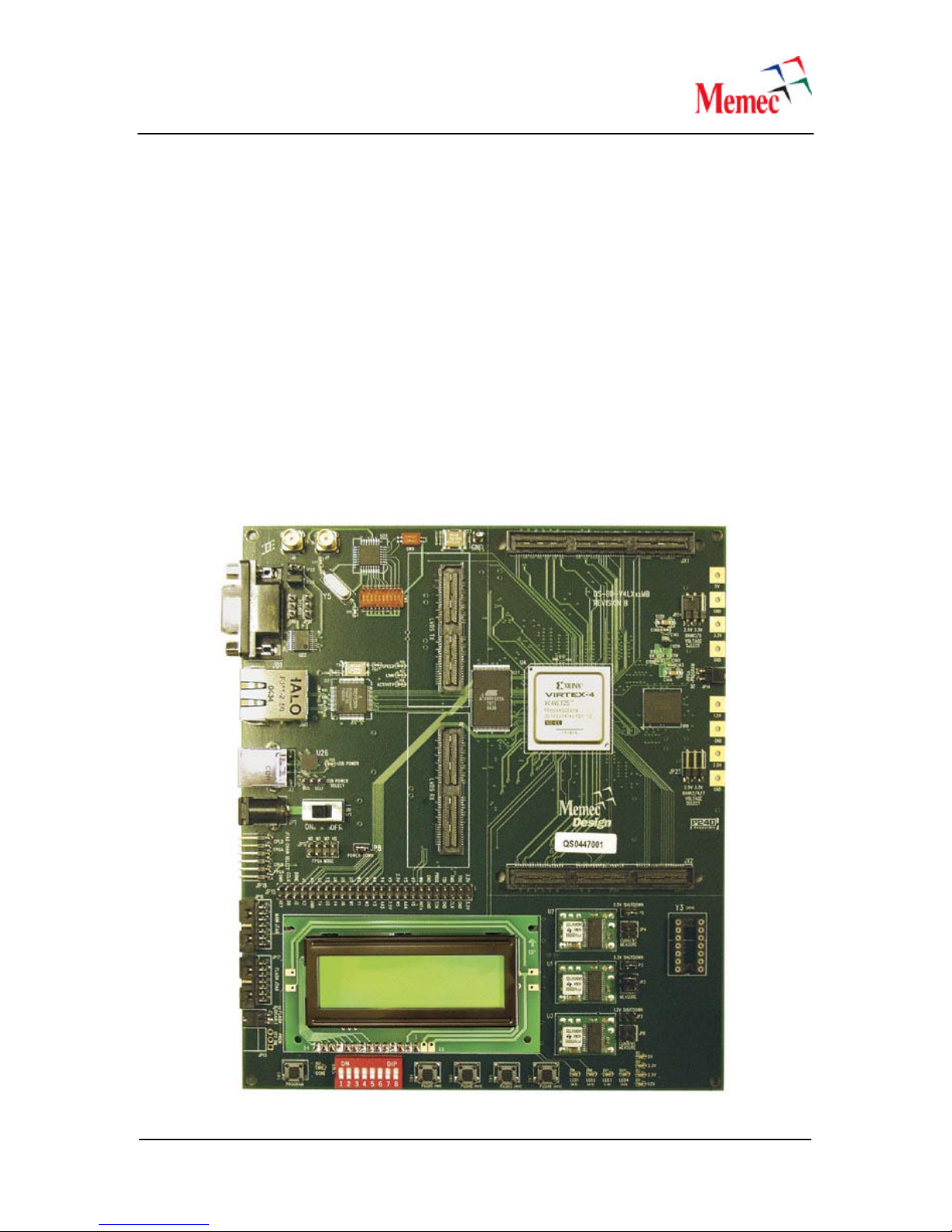
The Virtex -4 MB system board utilizes the Xilinx XC4VLX25/LX60/SX35 -10FF668C FPGA. The
board includes 64MB of DDR SDRAM, 4MB of Flash, 16-bit LVDS Trans mit and Receive ports,
programmable LVDS clock source, USB-RS232 Bridge, a 10/100 Ethernet PHY, 100 MHz clock
source, RS -232 port, and additional user support circuitry to develop a complete system. The
board also supports the Memec P240 expansion module standard, allowing application specific
expansion modules to be easily added.
2 The Virtex-4 MB System Board
December 20, 2005
Page 5
3 Functional Description
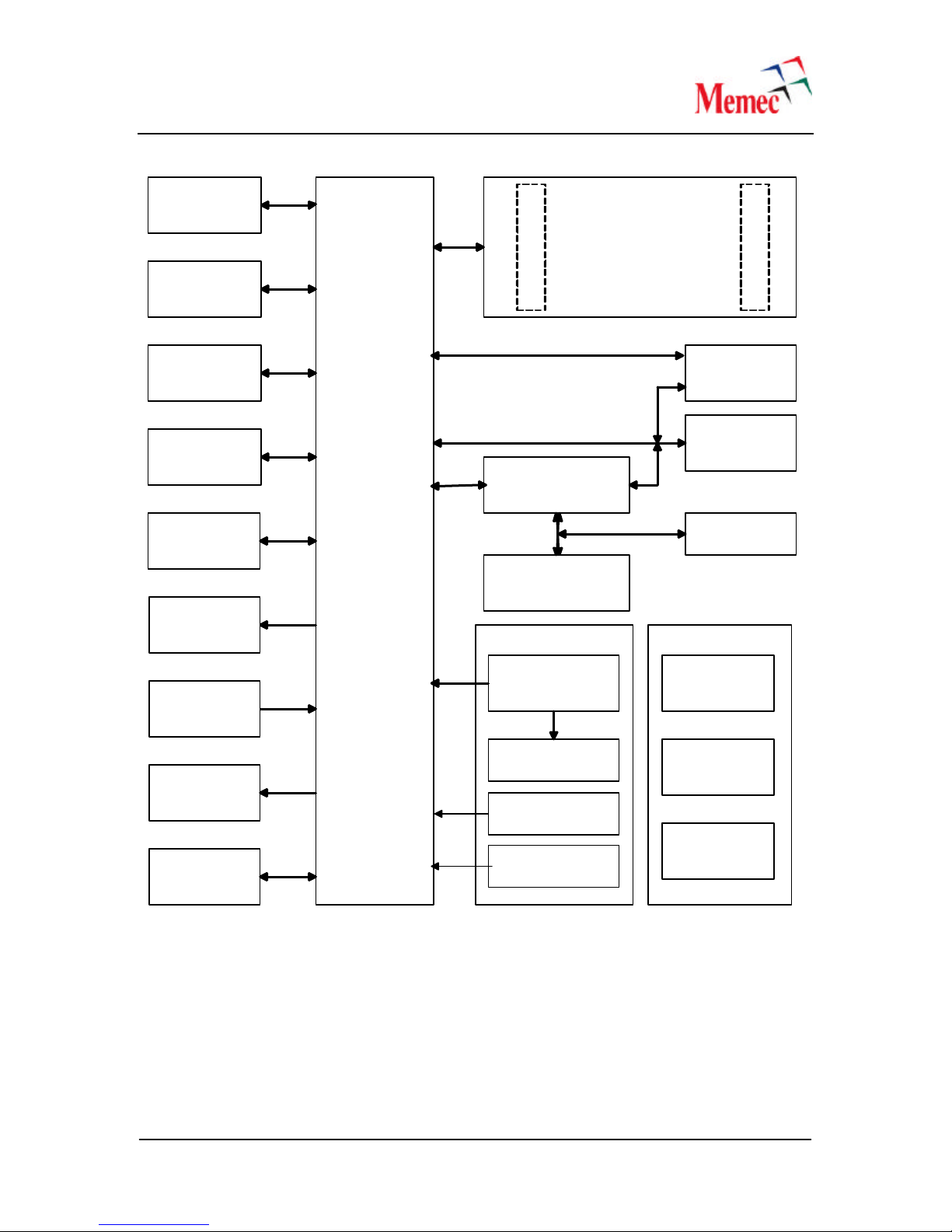
A high-level block diagram of the Virtex-4™ MB development platform is shown below followed
by a brief description of each sub-section. A list of features for this board is shown below:
• Xilinx XC4VLX25/LX60/SX35-10FF668 FPGA
• 64MB of DDR SDRAM
• 4MB of Flash
• 16-Bit LVDS Transmit and Receive Interfaces
• 10/100 Ethernet PHY
• Programmable LVDS Clock Source (25 -700 MHz)
• User LVDS Clock Outputs via Differential SMA Connectors
• On-board 100MHz LVTTL Oscillator
• On-board LVTTL Oscillator Socket (4/8-Pin Oscillators)
• P240 Connectors
• LCD Panel
• 32Mb Serial Flash for FPGA configuration
• PC4 JTAG Programming/Configuration Port
• SystemACE™ Module Connector
• RS232 Port
• Four User LEDs
• Four User Push Button Switches
• An 8-position DIP Switch
• USB-RS232 Bridge
December 20, 2005 2
Page 6
DDR SDRAM
(64MB)
Flash
(4MB)
P240 Module
132-Pin Connector
132-Pin Connector
16-Bit LVDS
Transmit &
Receive
10/100 PHY
RS232 Port
LCD Panel
User Switches
User LEDs
USB-RS232
Bridge
Virtex4 FPGA
XC4VLX25/LX60/
SX35
(FF668)
SAM Connector
Parallel Cable IV
XC9536XV
CPLD
Parallel Cable IV
Flash SPI Port
Atmel Serial Flash
(AT45DB321B-TC)
Voltage RegulatorsClock Sources
Programmable
LVDS Clock Source
SMA Clock Output 2.5V
LVTTL Clock
@100MHz
LVTTL OSC Socket
(4/8-Pin)
3.3V
Regulator
Regulator
1.2V
Regulator
JTAG Port
Figure 1 - Virtex-4 MB Development Platform Block Diagram
3.1 LVDS Interface
The Virtex-4 MB development board provides high -speed LVDS connectors supporting a SPI-4.2
interface. This interface consists of 36 LVDS signal pairs (72 FPGA signals) and 6 single-ended
signals. In addition to the SPI-4.2 interface, the LVDS interface is designed to support XSBI 16-bit
LVDS @644Mbps to support a 10GbE interface on the Virtex -4 MB development platform. The
following sections provide a brief description of the LVDS interface on this development board.
December 20, 2005 3
Page 7
3.1.1 SPI-4.2 Interface
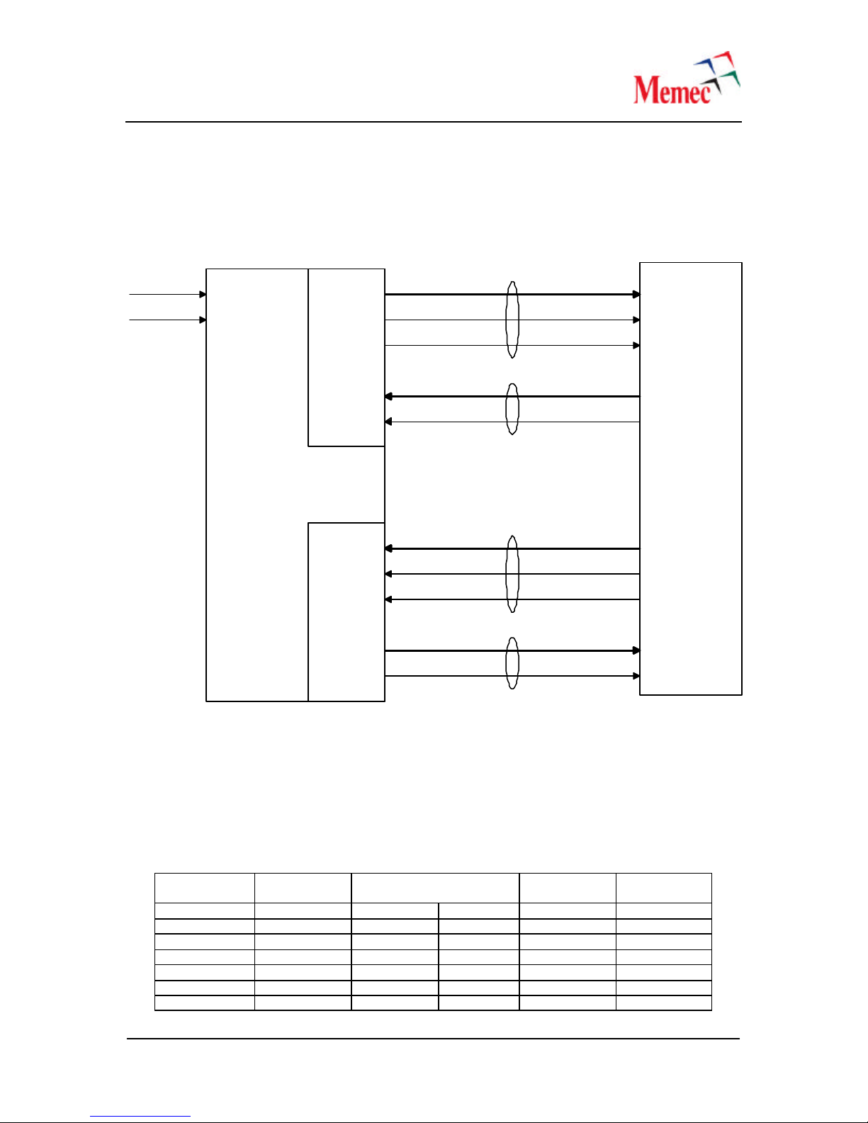
The Virtex-4 MB development board provides a SPI-4.2 via a 16-bit parallel LVDS electrical
interface. The following figure shows the SPI-4.2 interface on the board. The transmit and receive
interface of the SPI-4.2 are implemented using LVDS signals while the status flow cont rol signals
are implemented using single-ended LVTTL signals.
LVDS Signals
SysClk_P
SysClk_N
Transmit
Link Layer
Virtex-4 FPGA
4VLX25-FF668
TDat[15:0]
TDClk
TCtl
TStat[1:0]
TSClk
LVTTL Signals
TDat[15:0]
TDClk
TCtl
TStat[1:0]
TSClk
LVDS
Connectors
LVDS Signals
RDat[15:0]
RDClk
RCtl
RStat[1:0]
RSClk
Receive
Link Layer
RDat[15:0]
RDClk
RCtl
RStat[1:0]
RSClk
LVTTL Signals
Figure 2- SPI-4.2 Interface
3.1.2 SPI-4.2 Pin Assignments
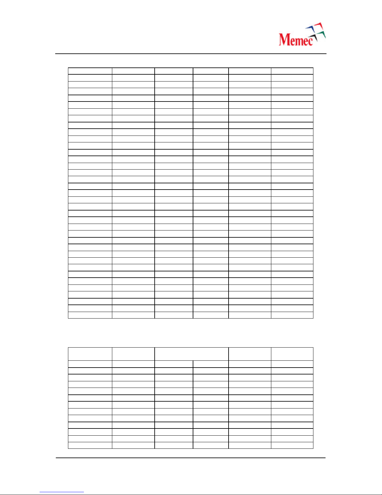
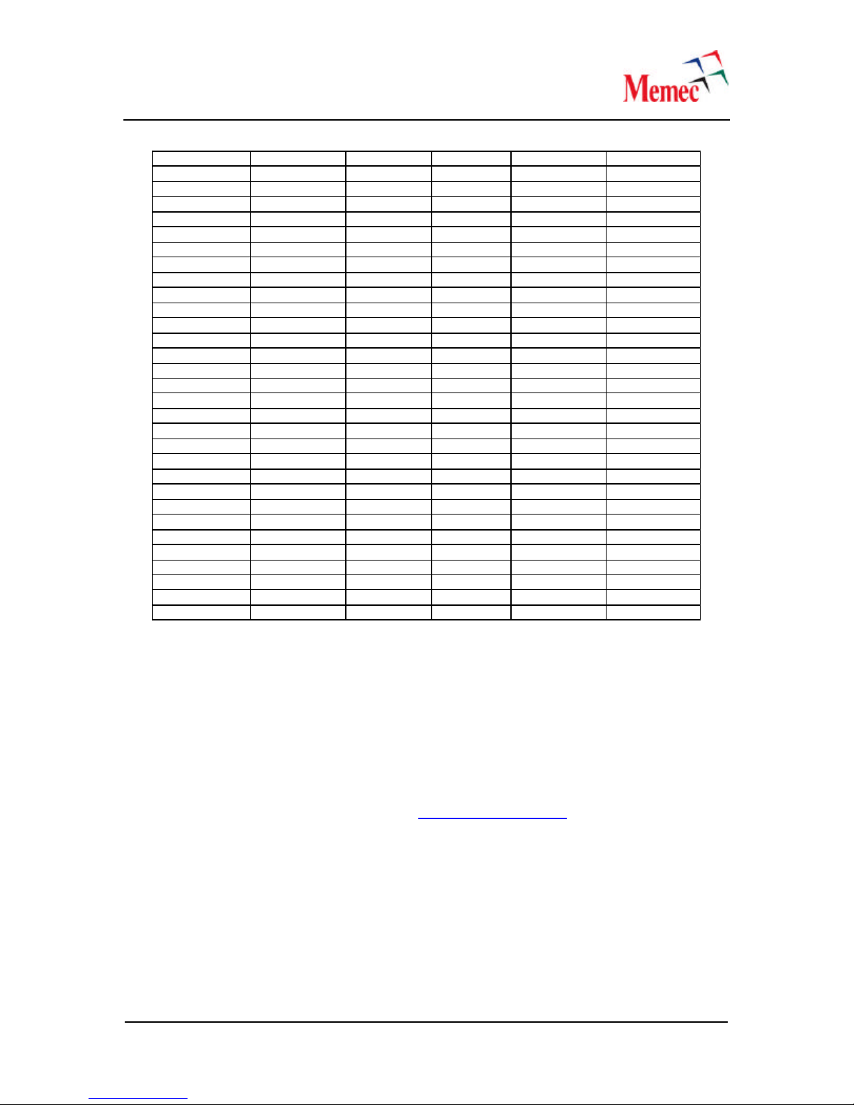
The following table shows the SPI-4.2 pin assignments for the 4VLX25/LX60/SX35 FPGA in the
FF668-pin package. These pin assignments must be used in the board design in order to meet
the SPI-4.2 interface core requirements.
Table 1– SPI-4.2 Transmit Pin Assignments
Virtex-4 Pin # LVDS Signal
Name
5.0V 1 2 5.0V
5.0V 3 4 5.0V
GND 5 6 GND
3.3V 7 8 3.3V
3.3V 9 10 3.3V
GND 11 12 GND
2.5V 13 14 2.5V
J4 Connector Pin #
LVDS TX
LVDS Signal
Name
Virtex-4 Pin #
December 20, 2005 4
Page 8
2.5V 15 16 2.5V
GND 17 18 GND
R8 TSCLK 19 20 NC
NC 21 22 NC
GND 23 24 GND
T8 TSTAT0 25 26 NC
T7 TSTAT1 27 28 NC
GND 29 30 GND
A7 TDat_N(15) 31 32 TDat_N(14) D7
A8 TDat_P(15) 33 34 TDat_P(14) D8
GND 35 36 GND
E10 TDat_N(13) 37 38 TDat_N(12) A5
F10 TDat_P(13) 39 40 TDat_P(12) A6
G8 TDat_N(11) 41 42 TDat_N(10) C7
F8 TDat_P(11) 43 44 TDat_P(10) B7
GND 45 46 GND
D5 TDat_N(9) 47 48 TDat_N(8) B9
C5 TDat_P(9) 49 50 TDat_P(8) A9
GND 51 52 GND
B3 TDat_N(7) 53 54 TDat_N(6) D4
A3 TDat_P(7) 55 56 TDat_P(6) C4
GND 57 58 GND
D6 TDat_N(5) 59 60 TDat_N(4) E5
E7 TDat_P(5) 61 62 TDat_P(4) E6
GND 63 64 GND
G7 TDat_N(3) 65 66 TDat_N(2) C1
F7 TDat_P(3) 67 68 TDat_P(2) C2
GND 69 70 GND
H7 TDat_N(1) 71 72 TDat_N(0) E4
H8 TDat_P(1) 73 74 TDat_P(0) D3
GND 75 76 GND
C8 TCtl_N 77 78 TDCLK_N F9
D9 TCtl_P 79 80 TDCLK_P E9
GND 81 82 GND
GND 83 84 GND
GND 85 86 GND
GND 87 88 GND
Virtex-4 Pin # LVDS Signal
5.0V 1 2 5.0V
5.0V 3 4 5.0V
GND 5 6 GND
3.3V 7 8 3.3V
3.3V 9 10 3.3V
GND 11 12 GND
2.5V 13 14 2.5V
2.5V 15 16 2.5V
GND 17 18 GND
U5 RSCLK 19 20 NC
NC 21 22 NC
GND 23 24 GND
J1 RSTAT0 25 26 NC
Table 2 – SPI -4.2 Receive Pin Assignments
Name
J5 Connector Pin #
LVDS RX
LVDS Signal
Name
Virtex-4 Pin #
December 20, 2005 5
Page 9
J2 RSTAT1 27 28 NC
GND 29 30 GND
AB4 RDat_N(15) 31 32 RDat_N(14) AB2
AC4 RDat_P(15) 33 34 RDat_P(14) AB3
GND 35 36 GND
AB5 RDat_N(13) 37 38 RDat_N(12) AC1
AC5 RDat_P(13) 39 40 RDat_P(12) AC2
AE3 RDat_N(11) 41 42 RDat_N(10) AD1
AF3 TDat_P(11) 43 44 RDat_P(10) AD2
GND 45 46 GND
AE4 RDat_N(9) 47 48 RDat_N(8) AC3
AF4 RDat_P(9) 49 50 RDat_P(8) AD3
GND 51 52 GND
AF5 RDat_N(7) 53 54 RDat_N(6) Y7
AF6 RDat_P(7) 55 56 RDat_P(6) AA7
GND 57 58 GND
Y9 RDat_N(5) 59 60 RDat_N(4) AD4
AA9 RDat_P(5) 61 62 RDat_P(4) AD5
GND 63 64 GND
Y1 RDat_N(3) 65 66 RDat_N(2) V7
Y2 RDat_P(3) 67 68 RDat_P(2) W7
GND 69 70 GND
Y8 RDat_N(1) 71 72 RDat_N(0) AA10
AA8 RDat_P(1) 73 74 RDat_P(0) Y10
GND 75 76 GND
AA1 RCtl_N 77 78 RDCLK_N AF10
AB1 RCtl_P 79 80 RDCLK_P AF11
GND 81 82 GND
GND 83 84 GND
GND 85 86 GND
GND 87 88 GND
3.1.3 LVDS Connector
The design of the SPI-4.2 interface requires use of a high -speed and high quality connector. The
V4MB development board uses the SAMTEC QSE type connector for this interface. The QSE-
040-01-L-Dx-A connector from SAMTEC provides up to 28 LVDS signal connections in addition
to an adequate number of ground connections for improving the signal quality. Two of these
connectors are used on the V4MB development board to implement the SPI-4.2 interface. In
addition, a mating LVDS extension cable is available from Samtec (part number #EQCD-040-
06.00-TTR-TBL -1). The following figure shows the QSE type connector from SAMTEC (the
picture is obtained from the SAMTEC web site (http://www.samtec.com/).
December 20, 2005 6
Page 10
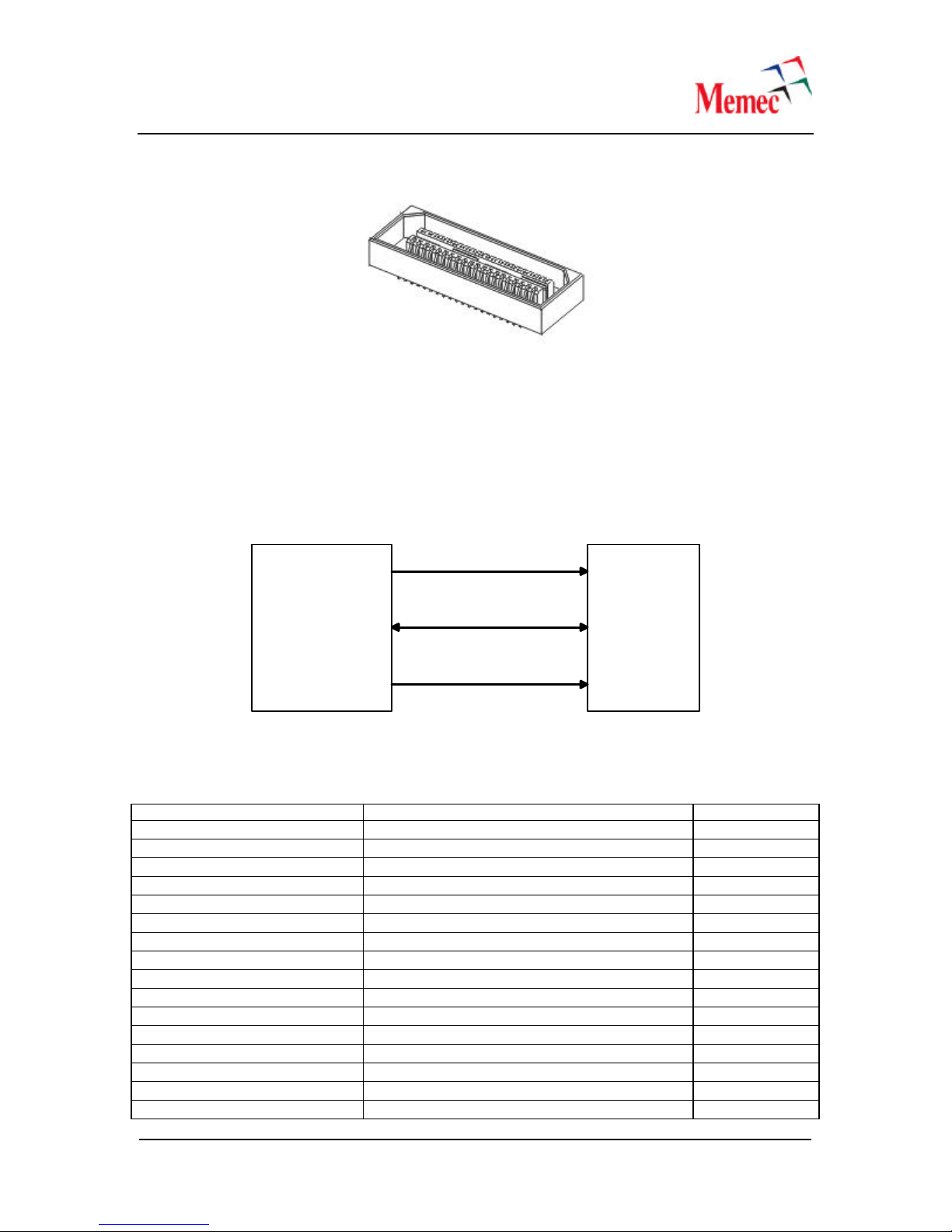
Figure 3 – SAMTEC QSE Type Connector for the SPI-4.2 Interface
3.2 DDR SDRAM
The Virtex-4™ MB development board provides 64MB of DDR SDRAM memory (x16). A highlevel block diagram of the DDR SDRAM interface is shown below followed by a table describing
the SDRAM memory interface signals.
Address[0:12]
Virtex-4 FPGA
LX25/LX60-FF668
Figure 4 – DDR SDRAM Interface
Table 3 – DDR SDRAM Interface Pin Assignments
Signal Name Description FPGA Pin #
ddr_addr[0] Address 0
ddr_addr[1] Address 1
ddr_addr[2] Address 2
ddr_addr[3] Address 3
ddr_addr[4] Address 4
ddr_addr[5] Address 5
ddr_addr[6] Address 6
ddr_addr[7] Address 7
ddr_addr[8] Address 8
ddr_addr[9] Address 9
ddr_addr[10] Address 10
ddr_addr[11] Address 11
ddr_addr[12] Address 12
ddr_dq[0] Data 0
ddr_dq[1] Data 1
ddr_dq[2] Data 2
Data[0:15]
Control
DDR SDRAM
(64MB)
N23
K23
N24
J23
V23
P23
U23
P24
T24
R23
K24
T23
R24
K20
J20
L20
December 20, 2005 7
Page 11
ddr_dq[3] Data 3
ddr_dq[4] Data 4
ddr_dq[5] Data 5
ddr_dq[6] Data 6
ddr_dq[7] Data 7
ddr_dq[8] Data 8
ddr_dq[9] Data 9
ddr_dq[10] Data 10
ddr_dq[11] Data 11
ddr_dq[12] Data 12
ddr_dq[13] Data 13
ddr_dq[14] Data 14
ddr_dq[15] Data 15
ddr_ba[0] Bank Select 0
ddr_ba[1] Bank Select 1
ddr_dm[0] Write Mask0
ddr_dm[1] Write Mask1
ddr_dqs[0] Data Strobe0
ddr_dqs[1] Data Strobe1
ddr_csn Chip Select L24
ddr_rasn Row Address Strobe M21
ddr_casn Column Address Strobe M23
ddr_wen Write Enable L21
ddr_clk Clock
ddr_clkn Clock
ddr_clke Clock Enable K21
J21
M20
K22
N20
J22
T21
P20
T20
T19
U22
P22
U21
U20
L23
M24
M22
N22
M19
N19
R20
R19
3.3 Flash
The Virtex-4™ MB development board provides 4MB of flash memory (x16). A high-level block
diagram of the flash interface is shown below followed by a table describing the flash memory
interface signals.
Address[0:20]
Virtex-4 FPGA
LX25-FF668
Figure 5 – Flash Interface
Table 4 – Flash Interface Pin Assignments
Signal Name Description FPGA Pin #
flash_addr[0] Address 0
flash_addr[1] Address 1
flash_addr[2] Address 2
Data[0:15]
Control
Flash
(4MB)
M2
T6
R5
December 20, 2005 8
Page 12
flash_addr[3] Address 3
flash_addr[4] Address 4
flash_addr[5] Address 5
flash_addr[6] Address 6
flash_addr[7] Address 7
flash_addr[8] Address 8
flash_addr[9] Address 9
flash_addr[10] Address 10
flash_addr[11] Address 11
flash_addr[12] Address 12
flash_addr[13] Address 13
flash_addr[14] Address 14
flash_addr[15] Address 15
flash_addr[16] Address 16
flash_addr[17] Address 17
flash_addr[18] Address 18
flash_addr[19] Address 19
flash_addr[20] Address 20
flash_d[0] Data 0
flash_d[1] Data 1
flash_d[2] Data 2
flash_d[3] Data 3
flash_d[4] Data 4
flash_d[5] Data 5
flash_d[6] Data 6
flash_d[7] Data 7
flash_d[8] Data 8
flash_d[9] Data 9
flash_d[10] Data 10
flash_d[11] Data 11
flash_d[12] Data 12
flash_d[13] Data 13
flash_d[14] Data 14
flash_d[15] Data 15
flash_cen Chip Select
flash_oen Output Enable
flash_wen Write Enable
flash_rdy Ready
flash_reset Reset
P5
P6
P7
P8
N8
K6
J7
M7
M8
L8
K7
J4
J6
R3
N7
N5
L7
M6
P2
R2
U1
K3
L3
M4
N4
P3
R1
T1
K4
L4
M3
N3
P4
R4
M1
N2
J5
M5
K5
3.4 Clock Sources
The Clock Generation section of the Virtex-4 MB board provides all the necessary clocks for a
MicroBlaze processor, the I/O devices located on the board, as well as the DDR SDRAM
memory. In general, the clock sources on the board are grouped into two categories; differential
and single-ended clock sources. The differential clock sources are primarily used by the LVDS
interface, while the single-ended clock sources are used by the processor section.
An on-board 100MHz oscillator provides the system clock input to the processor section. This
100Mhz clock will be used by the Virtex-4 Digital Clock Managers (DCMs) to generate various
processor clocks. In addition to the above clock inputs, a socket is provided on the board that can
December 20, 2005 9
Page 13
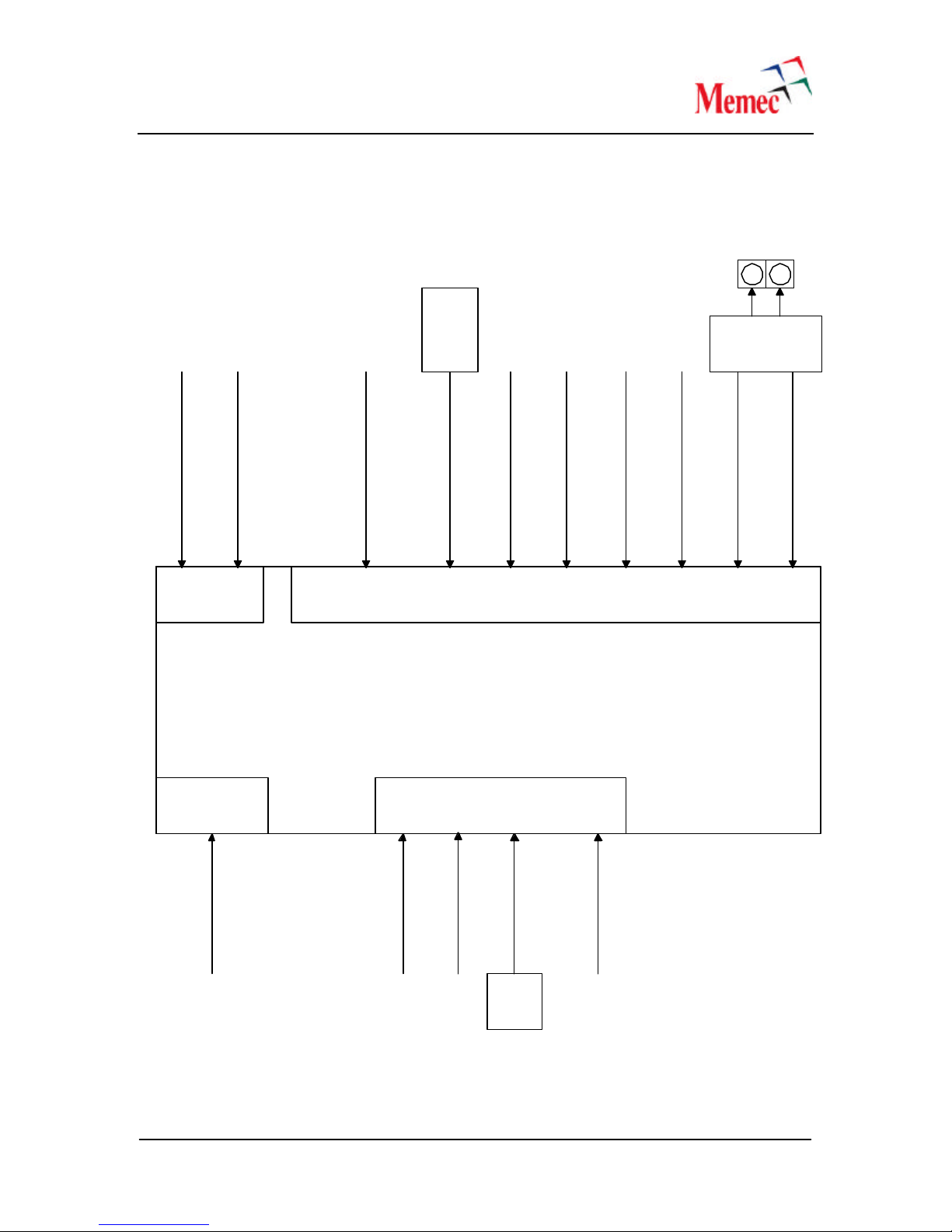
be used to provide single ended LVTTL clock input to the FPGA via an 8 or 4-pin oscillator. The
following figure shows the clock resources on the Virtex-4 MB development board.
SMA
Connectors
LVTTL
P240
Single-ended
CLock
DDR
Feedback
Clock
OSC
@100
MHz
P240
Differential
CLock
Programmable
LVDS Clock
Source
DDR_CLK
LIO_CLKIN_0
D12 E13
LIO_CLKIN_1
C15 B13 A16 B15
Bank 1 Bank 3
Bank 10
R8
CLK_100
XC4VL25/LX60-FF668
AF11AF10
ETH_RXC
Virtex-4™
Bank 4
AE14 AE10
ETH_TXC
LIO_CLKIN_P
B17 A17 A10 B10
LIO_CLKIN_N
CLK_PROG_P
CLK_PROG_N
SPI_TSCLK
SPI
Status
Clock
Figure 6 - Clock Sources on the Virtex-4 MB Board
December 20, 2005 10
SPI_RDCLK_N
SPI_RDCLK_P
CLK_SOCKET
OSC
Socket
SAM_CLK
SAM
CLock
Page 14
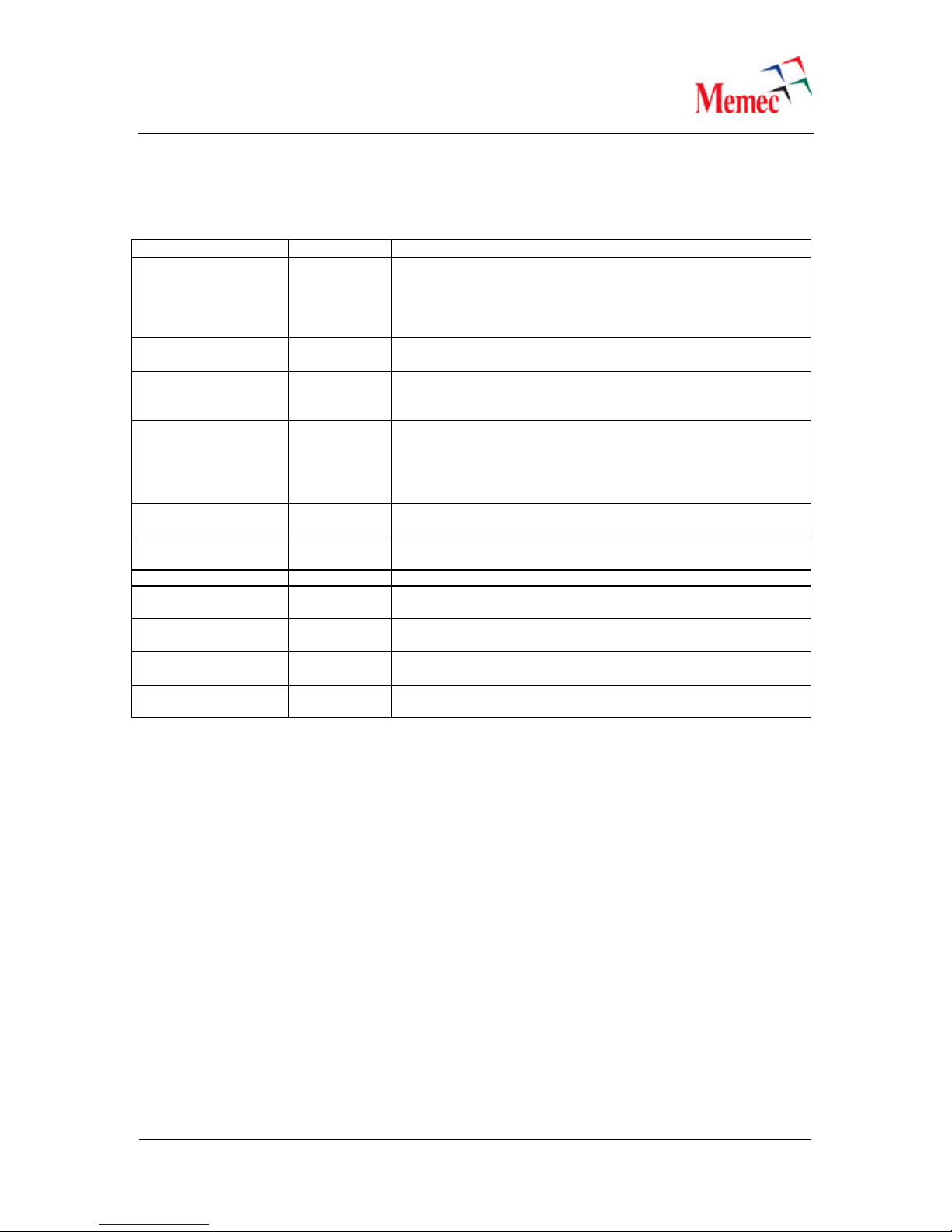
The following table provides a brief description of each clock input to the Virtex -4 FPGA.
Table 5 - Clock Inputs
Signal Name FPGA Pin # Description
CLK_PROG_P,
CLK_PROG_N
LIO_CLKIN_P,
LIO_CLKIN_N
LIO_CLKIN_0,
LIO_CLKIN_1
SPI_RDCLK_P,
SPI_RDCLK _N
DDR_CLK C15 DDR Feedback Clock Input – This clock input is connected to
CLK_100 B13 System Clock – This clock input is connected to a 100MHz
CLK_SOCKET AE14 LVTTL Clock Input – LVTTL socket on the Virtex -4 board.
SPI_TSCLK R8 SPI-4.2 Transmit Status Clock Input – This clock input is
ETH_RXC A16 Ethernet Receive Clock Input – This clock input is connected
ETH_TXC B15 Ethernet Transmit Clock Input – This clock input is connected
SAM_CLK AE10 SystemACE Module Clock Input – This clock input is
A10,
B10
B17,
A17
D12,
E13
AF11,
AF10
Positive and Negative Differential System Clock Inputs –
These clock inputs are connected to the output of an LVDS clock
synthesizer. This programmable clock source can generate a
clock frequency of 25 to 700MHz. Refer to the Programmable
LVDS Clock Source section for more information.
P240 Module Differential Clock Input – This clock input is
connected to the P240 connector located on the Virtex -4 board.
P240 Module Single-ended Clock Input s– These clock inputs
are connected to the P240 connector located on the Virtex -4
board.
Positive and Negative Differential SPI-4.2 Receive Clock
Inputs – These clock inputs are connected to the LVDS receive
connector on the Virtex-4 MB board. For the SPI-4.2
applications, these clock inputs are the SPI-4.2 receive clock
outputs.
the DDR clock.
LVTTL oscillator.
connected to the SPI-4.2 transmit status clock output.
to the Ethernet receive clock.
to the Ethernet transmit clock.
connected to the SystemACE Module connector.
3.4.1 Programmable LVDS Clock Source
A programmable LVDS clock synthesizer is used on the Virtex-4 MB development board to
generate a reference clock input to the LVDS interface. The use of this variable clock source,
allows designers to prototype various interconnect technologies with different clock source
requirements. The differential output port is also well suited for DSP applications when driving
external DACs or ADCs.
3.4.2 ICS8442 Programmable LVDS Clock Synthesizer
The Virtex-4 MB development board design uses the ICS8442 LVDS clock synthesizer for
generating various clock frequencies. A list of features included in the ICS8442 device is shown
below.
• Output frequency range: 25MHz to 700MHz
• RMS period jitter: 2.7ps (typical)
• Cycle-to-cycle jitter: 27ps (typical)
• Output rise and fall time: 650ps (maximum)
• Output duty cycle: 48/52
December 20, 2005 11
Page 15
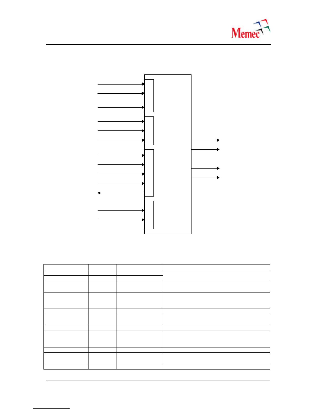
The following figure shows a high -level block diagram of the ICS8442 programmable LVDS clock
synthesizer.
M[0:8]
N[0:1]
nP_LOAD
S_DATA
S_CLOCK
S_LOAD
VCO_SEL
XTAL_SEL
TEST_CLK
MR
TEST
XTAL1
XTAL2
Parallel LoadSerial Load
ICS8442
Control Inputs
Clock Input
FOUT0
nFOUT0
CLKOUT0CLKOUT1
FOUT1
nFOUT1
Figure 7 – ICS8442 Clock Synthesizer
Table 6 – ICS8442 Clock Synthesizer Pin Description
Signal Name Direction Pull up/Pull down Description
M[0:4], M[6:8] Input Pull down
M[5] Input Pull up
N[0:1] Input Pull down The N divider inputs, latched on the rising edge
TEST Output The TEST output is active during the serial mode
MR Input Pull down Active high reset signal.
S_CLOCK Input Pull down Serial interface clock input. Data is shifted into
S_DATA Input Pull down Serial interface data input.
S_LOAD Input Pull down Serial interface load signal. The contents of the
TEST_CLK Input Pull down Test clock input.
nP_LOAD Input Pull down The rising edge of this signal is used to load the
XTAL1, XTAL2 Input Crystal clock input/output
The M divider inputs, latched on the rising edge
of the nP_LOAD signal.
of the nP_LOAD signal.
of operations. Please refer to the datasheet for
more information.
the device on the rising edge of this clock.
serial data shift register is loaded into the internal
dividers on the rising edge of this signal.
M and N divider inputs into the device.
December 20, 2005 12
Page 16
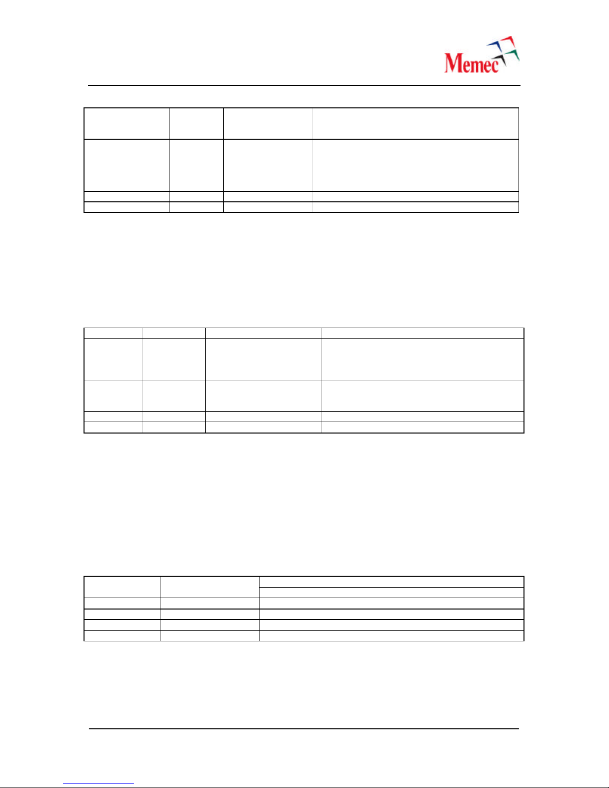
XTAL_SEL Input Pull up This signal is used to select between the crystal
and the TEST_CLK input to the device. When
this high, crystal is selected.
VCO_SEL Input Pull up This signal is used to place the internal PLL in
the bypass mode. When this signal is set to low,
the PLL is placed in the bypass mode. For
normal operations, this signal must be set to
high.
FOUT0, FOUT1 Output Positive LVDS clock outputs
nFOUT0, nFOUT1 Output Negative LVDS clock outputs
The Input Clock Select signals of the ICS8442 can be used to provide a reference clock input to
the device other than the 25MHz crystal oscillator (for test purposes). The following table shows
how these Input Clock Select signals are used to generate the output clock or to test the ICS8442
device. Please refer to the ICS8442 datasheet for more information on using the TEST_CLK
clock input.
Table 7 – Input Clock Select Signal Description
VCO_SEL XTAL_SEL Reference Clock Input FOUT[0:1]
0 0 TEST_CLK TEST_CLK/N (the TEST_CLK must be between
10 and 25MHz). This mode can be used to test
the ICS8442 device by routing the input clock to
the outputs.
0 1 25MHz crystal 25MHz crystal/N (This mode can be used to test
the ICS8442 device by routing the 25MHz
crystal clock to the outputs).
1 0 TEST_CLK ICS8442 PLL Output/N (Normal Operation)
1 1 25MHz crystal ICS8442 PLL Output/N (Normal Operation)
3.4.3 ICS8442 Clock Generation
The ICS8442 output clocks are generated based on the following formula (assuming the crystal
clock input is set to 25MHz):
FOUT[0:1] = 25 x M/N
Where 8 < M < 28 and N can take a value of 1, 2, 4, or 8. The variable M is determined by setting
the binary number M[0:8] while N is set according to the following table:
Table 8 – ICS8442 N Settings
Output Clock Frequency Range (MHz) N[1:0] N
Minimum Maximum
00 1 200 700
01 2 100 350
10 4 50 175
11 8 25 87.5
For example, to generate a 62.5MHz clock, N[1:0] will be set to “10” (it can also be set to “11”
since either one will be the correct frequency range for the 62.5MHz clock) and M will be set to
“000001010” (decimal 10). So, from the above formula:
FOUT[0:1] = 25 x 10/4 = 62.5Mhz
December 20, 2005 13
Page 17
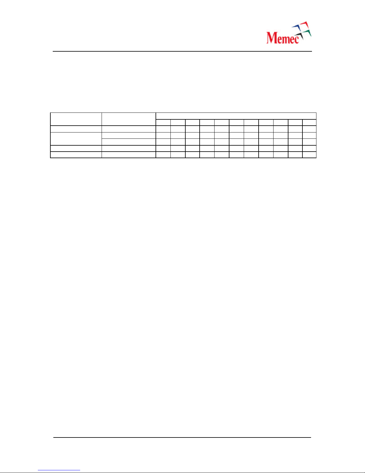
The following table shows how the M and N values can be set to generate a clock source for a
few commo n applications. All the values for M and N are based on the 25MHz crystal clock input
to the ICS8442 device. A complete list of frequencies generated by the ICS8442 (based on a
25MHz input clock) is provided in the following sections.
Table 9 – Examples of the ICS8442 M and N Settings
FOUT0 and
Technology
Gigabit Ethernet 62.5 0 0 0 0 0 1 0 1 0 1 0
Infiniband 125 0 0 0 0 1 0 1 0 0 1 0
XAUI 156.25 0 0 0 0 1 1 0 0 1 1 0
FOUT1 (MHz)
53.125 0 0 0 0 1 0 0 0 1 1 1 Fiber Channel
106.25 0 0 0 0 1 0 0 0 1 1 0
M8 M7 M6 M5 M4 M3 M2 M1 M0 N1 N0
ICS8442 M and N Settings Interconnect
3.4.4 ICS8442 Programming Modes
The ICS8442 provides two different methods of programming the M and N values into the device;
a Parallel Mode and a Serial Mode. In parallel mode, M and N values are programmed into the
device when the nP_LOAD signal pulses low. In the serial mode, the I2C pins (S_DATA and
S_CLOCK) along with the S_LOAD signal are used to shift the M and N values into the device.
Please refer to the ICS8442 datasheet for more information on programming modes of loading
the M and N values into the device.
3.4.5 ICS8442 M and N Settings
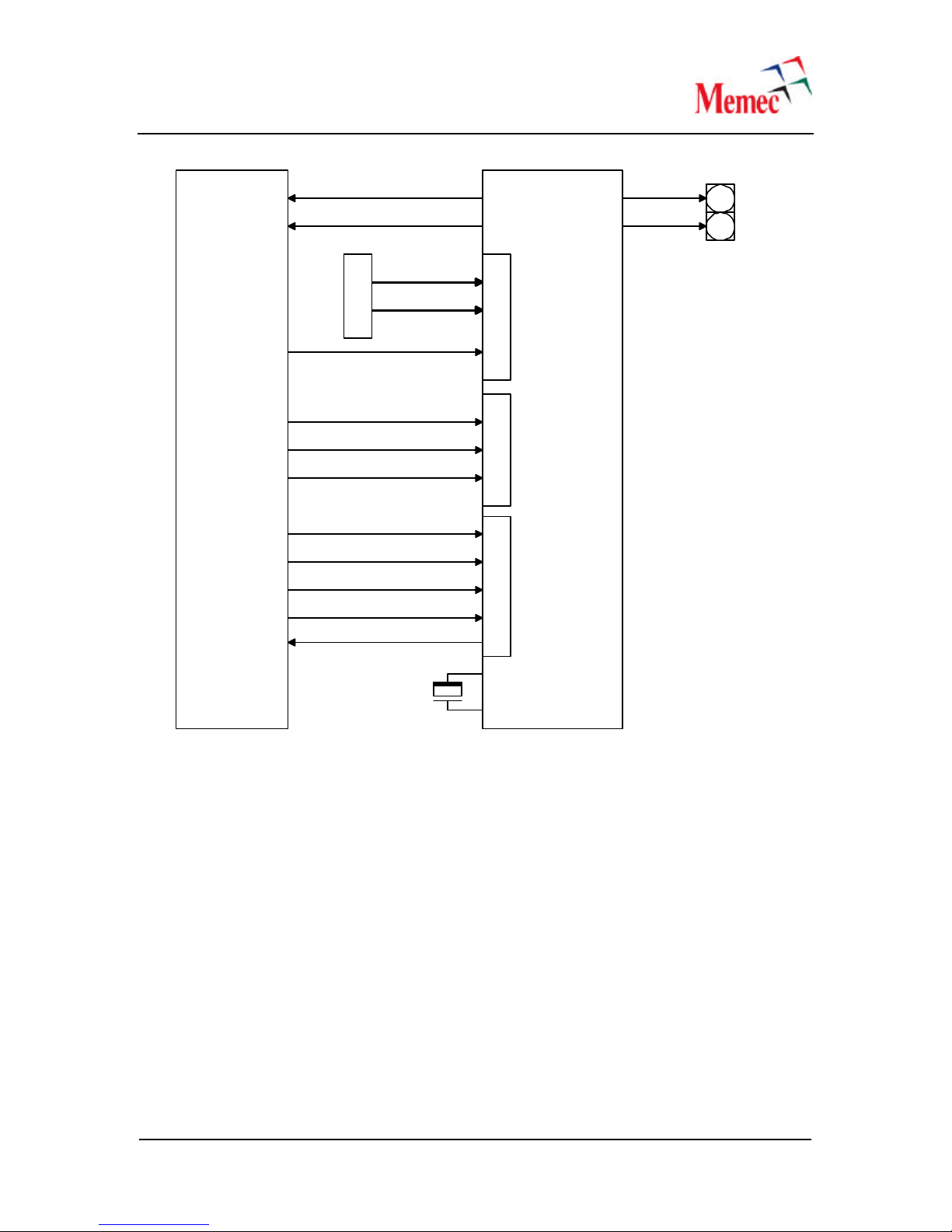
The following figure shows how the ICS8442 programmable LVDS clock synthesizer is used on
the Virtex-4 MB board. DIP Switches are provided on the board for manual setting of the M and N
values.
December 20, 2005 14
Page 18
Virtex-4
FPGA
DIP Switch
VCO_SEL
XTAL_SEL
TEST_CLK
FOUT0
nFOUT0
M[0:8]
N[0:1]
nP_LOAD
S_DATA
S_CLOCK
S_LOAD
MR
TEST
CLKOUT0
Parallel LoadSerial Load
ICS8442
Control Inputs
FOUT1
nFOUT1
CLKOUT1
SMA
Connectors
25Mhz
Figure 8 – ICS8442 Clock Synthesizer Interface to the FPGA
As shown in the above figure, the ICS8442 device outputs two identical LVDS clock sources. One
of these clock sources can be used to provide the reference clock input to the LVDS interface on
the Virtex-4 MB development board, while the other clock output can be used to trigger a scope
during testing. The second output could also be used to provide a low jitter, LVDS clock source
to a user board, such as the P240 module.
December 20, 2005 15
Page 19
CLK_PROG_P
Virtex-4
FPGA
CLK_PROG_N
CONTROL
SW3SW9
CLKOUT0
ICS8442
M[8:0]N1:0]
CLKOUT1
25Mhz
SMA
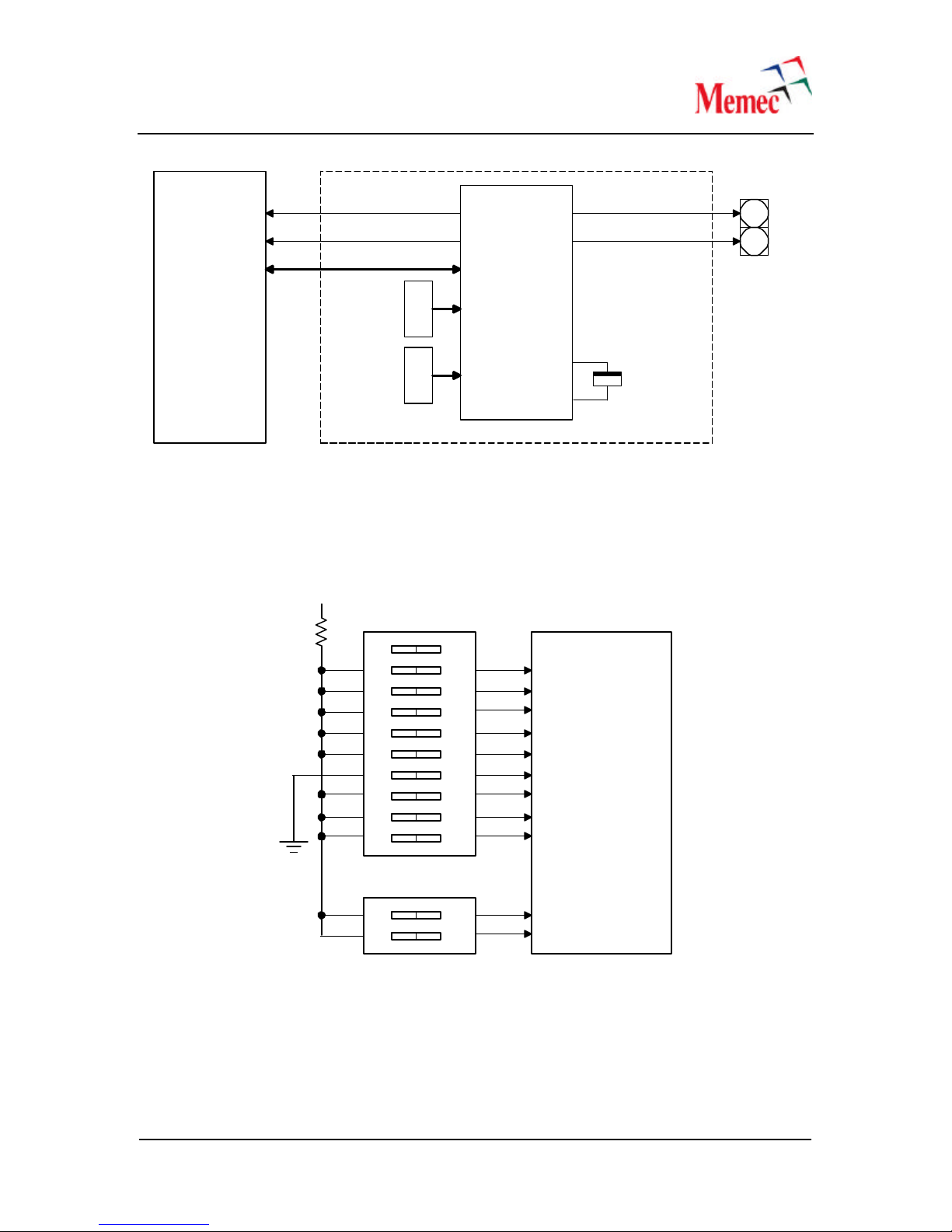
Figure 9 – ICS8442 Clock Synthesizer M and N DIP Switches
The following tables show the DIP Switch settings for M and N selections. Please refer to Table 6
for the information on pull-up and pull -down resistors provided internal to the ICS8442 device for
the M and N input signals.
3.3V
SW3
ON
OFF
10
9
8
7
6
5
4
3
2
1
M0
M1
M2
M3
M4
M5
Synthesizer
M6
M7
M8
Connectors
Figure 10 – M and N DIP Switches for the Synthesizers
December 20, 2005 16
ON
SW9
OFF
2
1
N0
N1
Page 20
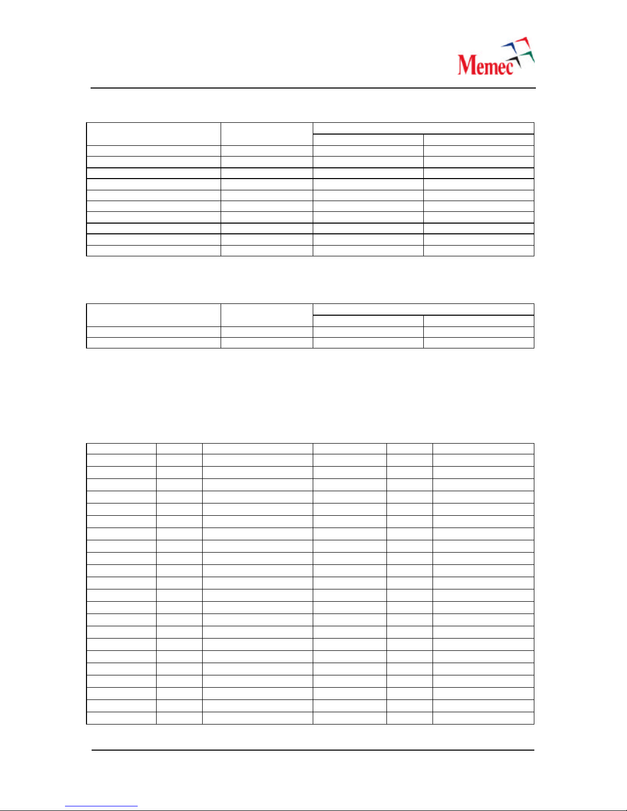
Table 10 – DIP Switch Setting for M[8:0]
Switch Position
OFF ON
SW1, SW10, and SW2
DIP1 M8 0 1
DIP2 M7 0 1
DIP3 M6 0 1
DIP4 M5 1 0 Note (1)
DIP5 M4 0 1
DIP6 M3 0 1
DIP7 M2 0 1
DIP8 M1 0 1
DIP9 M0 0 1
DIP10 Unused NA NA
M[8:0]
Note(1) – The polarity of M5 (DIP4) is the opposite of all other DIP switch positions.
Table 11 – DIP Switch Setting for N[1:0]
Switch Position
OFF ON
SW9, SW11, and SW13
DIP1 N1 0 1
DIP2 N0 0 1
N[1:0]
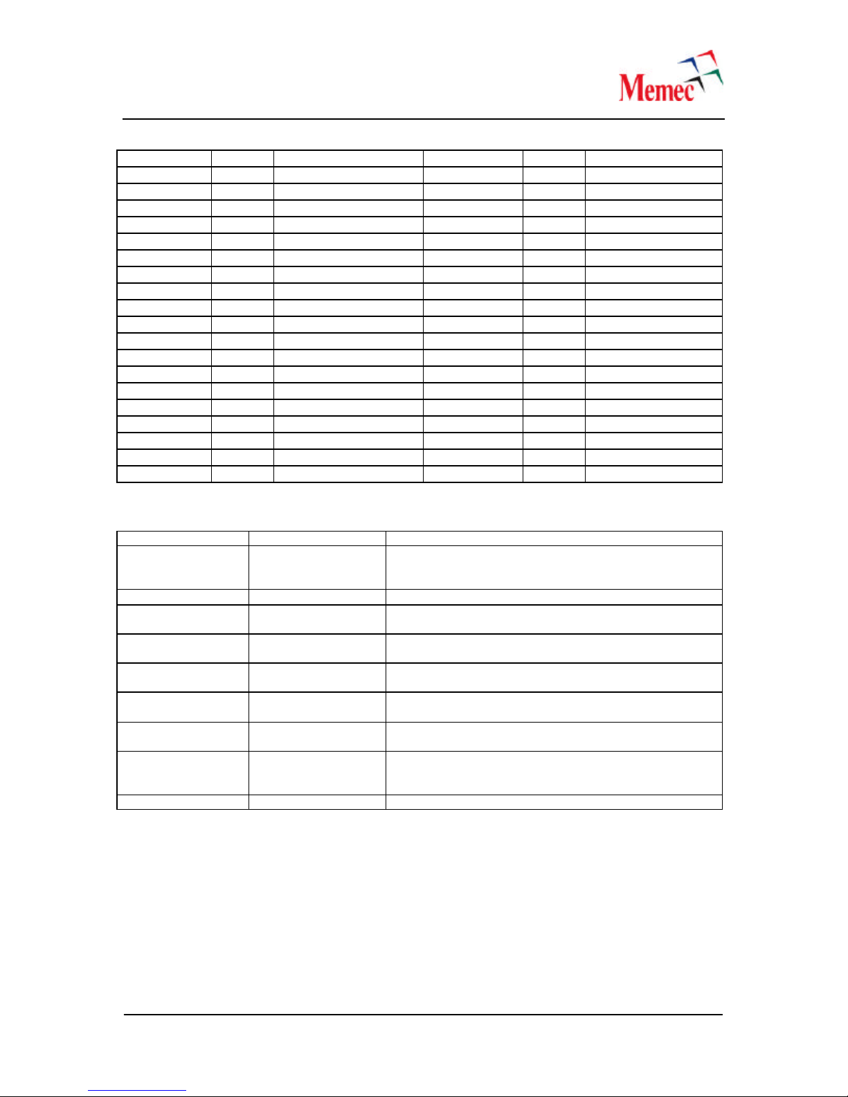
The following table shows a complete list of frequencies generated by the ICS8442 device based
on a 25MHz crystal reference clock input.
Table 12 – Synthesizer Clock Ou tputs for M and N Values
M[8:0] N[1:0] FOUT[1:0] (MHz) M[8:0] N[1:0] FOUT[1:0] (MHz)
000001000 11 25 (Min) 000011000 10 150
000001001 11 28.125 000011001 10 156.25
000001010 11 31.25 000001101 01 162.5
000001011 11 34.375 000011010 10 162.5
000001100 11 37.5 000011011 10 168.75
000001101 11 40.625 000001110 01 175
000001110 11 43.75 000011100 10 175
000001111 11 46.875 000001111 01 187.5
000001000 10 50 000001000 00 200
000010000 11 50 000010000 01 200
000010001 11 53.125 000010001 01 212.5
000001001 10 56.25 000001001 00 225
000010010 11 56.25 000010010 01 225
000010011 11 59.375 000010011 01 237.5
000001010 10 62.5 000001010 00 250
000010100 11 62.5 000010100 01 250
000010101 11 65.625 000010101 01 262.5
000001011 10 68.75 000001011 00 275
000010110 11 68.75 000010110 01 275
000010111 11 71.875 000010111 01 287.5
000001100 10 75 000001100 00 300
000011000 11 75 000011000 01 300
December 20, 2005 17
Page 21
000011001 11 78.125 000011001 01 312.5
000001101 10 81.25 000001101 00 325
000011010 11 81.25 000011010 01 325
000011011 11 84.375 000011011 01 337.5
000001110 10 87.5 000001110 00 350
000011100 11 87.5 000011100 01 350
000001111 10 93.75 000001111 00 375
000001000 01 100 000010000 00 400
000010000 10 100 000010001 00 425
000010001 10 106.25 000010010 00 450
000001001 01 112.5 000010011 00 475
000010010 10 112.5 000010100 00 500
000010011 10 118.75 000010101 00 525
000001010 01 125 000010110 00 550
000010100 10 125 000010111 00 575
000010101 10 131.25 000011000 00 600
000001011 01 137.5 000011001 00 625
000010110 10 137.5 000011010 00 650
000010111 10 143.75 000011011 00 675
000001100 01 150 000011100 00 700 (Max)
Table 13 – FPGA Pin Assignments for the Synthesizer Interface
Signal Name Virtex-4 Pin # Comments
SYNTH_PLOAD V2 This input is used to load the M and N values into the
synthesizer using the parallel mode configuration along
with the DIP switch settings for M and N.
SYNTH_RESET K1 This input signal resets the synthesizer.
SYNTH_SCLK L1 This clock input is used to load the M and N values into
the synthesizer using serial mode configuration.
SYNTH_SDATA T4 Serial data input to the synthesizer for loading the M and
N values.
SYNTH_SLOAD T3 This input signal is used to load the M and N values into
the synthesiz er using the serial mode configuration.
SYNTH_TEST U2 A test clock input can be provided to the synthesizer using
this clock input.
SYNTH_VCOSEL V1 This input signal can be used to bypass the PLL for test
purposes.
SYNTH_XTALSEL U3 This input signal is used to select between the test clock
input and the on-board crystal as clock source to the
synthesizer.
SYNTH_DOUT K2 This output signal is used as the test clock output.
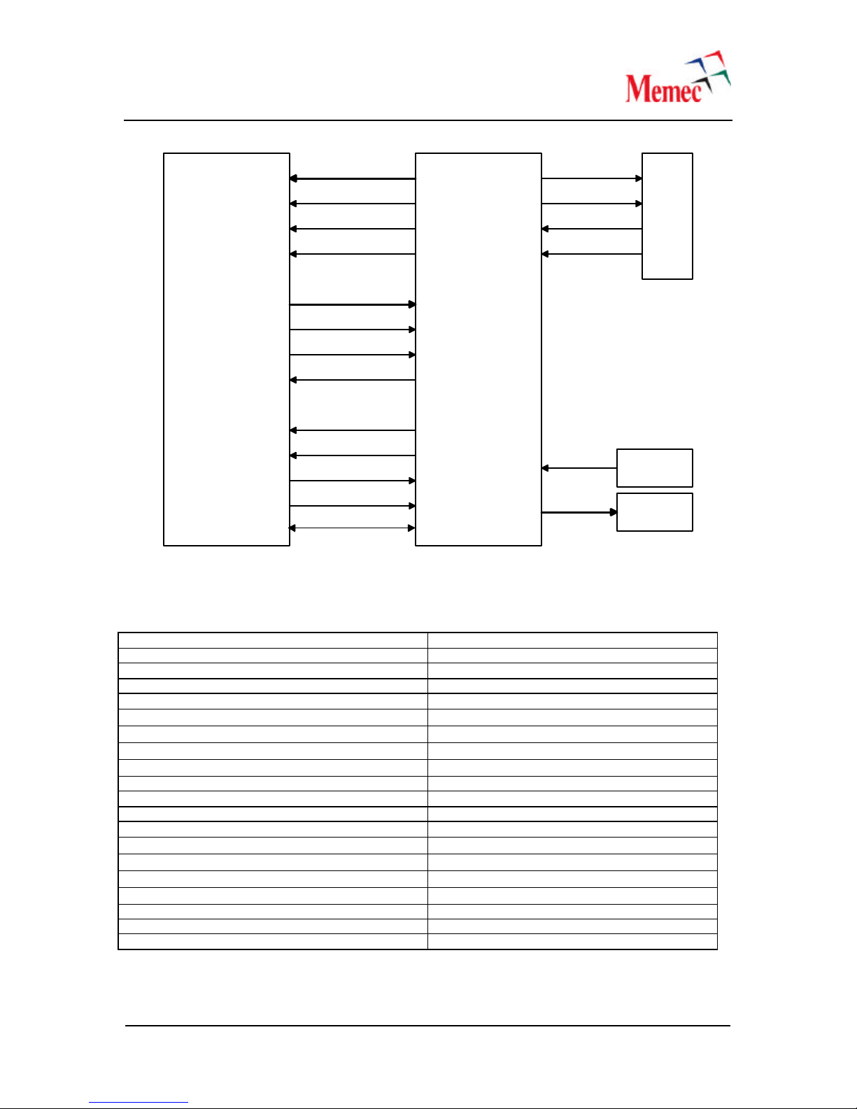
3.5 10/100 Ethernet PHY
The Virtex -4 MB development board provides a 10/100 Ethernet port for network connection. A
high-level block diagram of the 10/100 Ethernet interface is shown in the following figure followed
by FPGA pin assignments for this interface.
December 20, 2005 18
Page 22
TD+
TD-
RD+
RD-
Virtex-4
FPGA
ETH_RXD[0:3]
ETH_RXDV
ETH_RXER
ETH_RXC
ETH_TXD[0:3]
ETH_TXEN
ETH_TXER
ETH_TXC
ETH_COL
ETH_CRS
ETH_MDC
ETH_RESETn
ETH_MDIO
Broadcom
BCM5221
10/100 PHY
Figure 11 – 10/100 Etherne t Interface
The following table shows the FPGA pin assignments for the Ethernet interface.
Table 14 – Ethernet Pin Assignments
Signal Name Virtex-4 Pin #
ETH_TXC B15
ETH_RXC A16
ETH_CRS B14
ETH_RXDV H1
ETH_RXD[0]
ETH_RXD[1]
ETH_RXD[2]
ETH_RXD[3]
ETH_COL C14
ETH_RXER H2
ETH_TXEN G2
ETH_TXER G1
ETH_TXD[0]
ETH_TXD[1]
ETH_TXD[2]
ETH_TXD[3]
ETH_MDC F4
PHY_RESETn E3
ETH_MDIO H3
G4
G3
F3
H4
H5
H6
F1
C12
RJ45
Connector
(built-in magnetics)
Crystal
20Mhz
LEDs
December 20, 2005 19
Page 23
3.6 LCD Panel
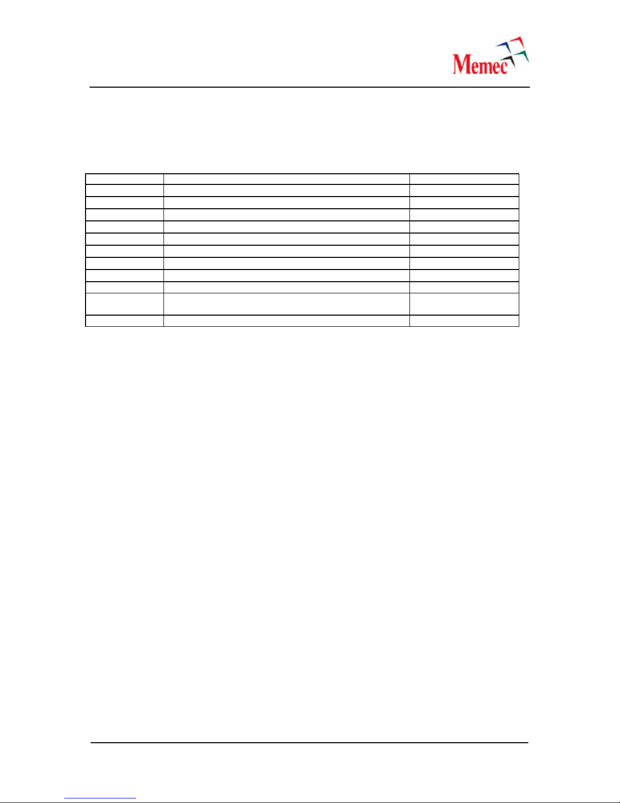
The Virtex-4 MB development board provides an 8-bit interface to a 2x16 LCD panel (MYTECH
MOC-16216B-B). The following table shows the LCD interface signals.
Table 15 – LCD Interface Signals
Signal Name Description Virtex-4 Pin #
D0
D1 LCD Data Bit 1
D2 LCD Dat a Bit 2
D3 LCD Data Bit 4
D4 LCD Data Bit 4
D5 LCD Data Bit 5
D6 LCD Data Bit 6
D7 LCD Data Bit 7
EN LCD Enable Signal L19
RW LCD Write Signal (this signal is connected to logic “0” on
RS LCD Register Select Signal N21
LCD Data Bit 0
the Virtex-4 MB board, enabling wr ite only cycles).
K25
P19
AC10
AB10
AF12
AE12
AC17
AB17
3.7 USB 2.0 to RS232 Port
The Virtex-4 MB development board implements a USB 2.0 port. This is accomplished using the
Cygnal CP2101 USB-to-UART Bridge Controller. The FPGA interfaces to the CP2102 as a
simple UART. The UART interface to the CP2102 can run at speeds ranging from 300 to 921,600
baud.
The CP2102 is a highly integrated USB -to-UART Bridge Controller, providing a simple solution for
USB serial communications using a minimum of components and PCB space. The CP2102
includes a USB 2.0 full -speed function controller, USB transceiver, oscillator, EEPROM, and
asynchronous serial data bus (UART) with full modem control signals in a compact 5mm X 5mm
MLP-28 package. No other external USB components are required.
The on-chip EEPROM may be used to customize the USB Vendor ID, Product ID, Product
Description String, Power Descriptor, Device Release Number, and Device Serial Number as
desired. The EEPROM is programmed on-board via the USB allowing the programming step to
be easily integrated into the product manufacturing and testing proces s.
Royalty-free Virtual COM Port (VCP) device drivers provided by Cygnal allow the Virtex -4 MB
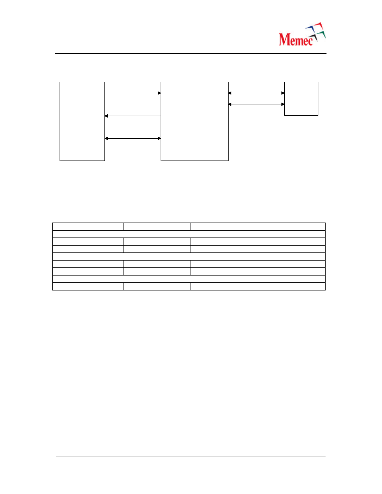
development board to appear as a COM port to PC applications. The CP2102 UART interface
implements all RS232 signals, including control and handshaking signals. These signals are
interfaced to the Virtex -4 FPGA as follows:
December 20, 2005 20
Page 24
USB
Connector
3
2
Virtex-4
FPGA
USB_SIN
USB_SOUT
USB_RESETn
USB2.0 to RS232
CP2102
RXD
TXD
DTR
D+
D-
D+
D-
Figure 12 – USB 2.0 to RS232 Serial Interface
The following table shows the RS232 interface signal names and their Virtex-4 FPGA pin
assignments.
Table 16- USB 2.0 to RS232 Port Signal Description
FPGA Signal Name Virtex-4 Pin # Description
RS232 Signals
USB_SIN R7 RS232 recei ve signal
USB_SOUT L6 RS232 transmit signal
USB 2.0 Signals
D+ NA USB D+ signal
D- NA USB D- signal
Common Signal
USB_RESETn R6 CP2102 reset signal
To use the USB port, the CP2102 device drivers must be installed. These drivers are included on
the Virtex-4 MB Development Kit CD and contained in the self-extracting file CP2101.exe. To
install the CP2101/2 virtual COM port device drivers, refer to Appendix A.
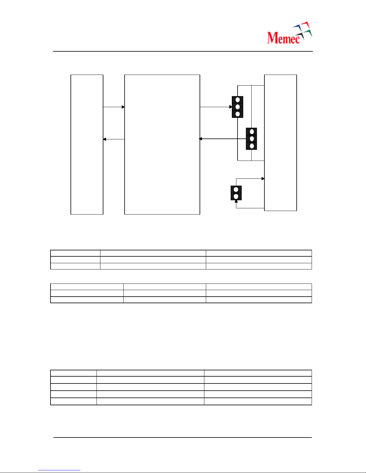
3.8 RS232
The Virtex -4 MB development board provides an RS232 interface with RX and TX signals and
jumpers for connecting the RTS and CTS signals. The following figure shows the RS232 interface
to the Virtex-4 LX25/LX60/SX35 FPGA.
December 20, 2005 21
Page 25
JP19
2
2 (RD)
RS232
Connector
3 (TD)
7 (RTS)
8 (CTS)
Virtex-4
FPGA
TXD
RXD
Din
Rout
RS232
Drivers
MAX3221
Dout
Rin
RD
TD
JP21
JP22
o
1
2
3
1
3
o
Figure 13 - RS232 Interface
Table 17 – RS232 Signals
Signal Name Description Virtex-4 Pin #
RS232_RXD Received Data, RD U4
RS232_TXD Transmit Data, TD V4
Table 18 - RS232 Jumper Settings
Mode of Operation JP19 JP21
DCE Install a jumper on pins 2-3 Install a jumper on pins 1-2
DTE Install a jumper on pins 1-2 Install a jumper on pins 2-3
A Jumper must be installed on JP22, if RTS and CTS signal connections are needed.
3.9 User DIP and PB Switches
The Virtex-4 MB development board provides four user push button switches as described in the
following table. An active low signal is generated when a given switch is pressed.
Table 19 – Push Button Switch Pin Assignments
Signal Name Description Virtex-4 Pin #
PUSH1 SW5
PUSH2 SW6
PUSH3 SW7
PUSH4 SW8
The Virtex-4 MB development board provides an 8-position DIP switch as described in the
following table. An active low signal is generated when a given switch is ON.
December 20, 2005 22
E2
E1
G10
G9
Page 26
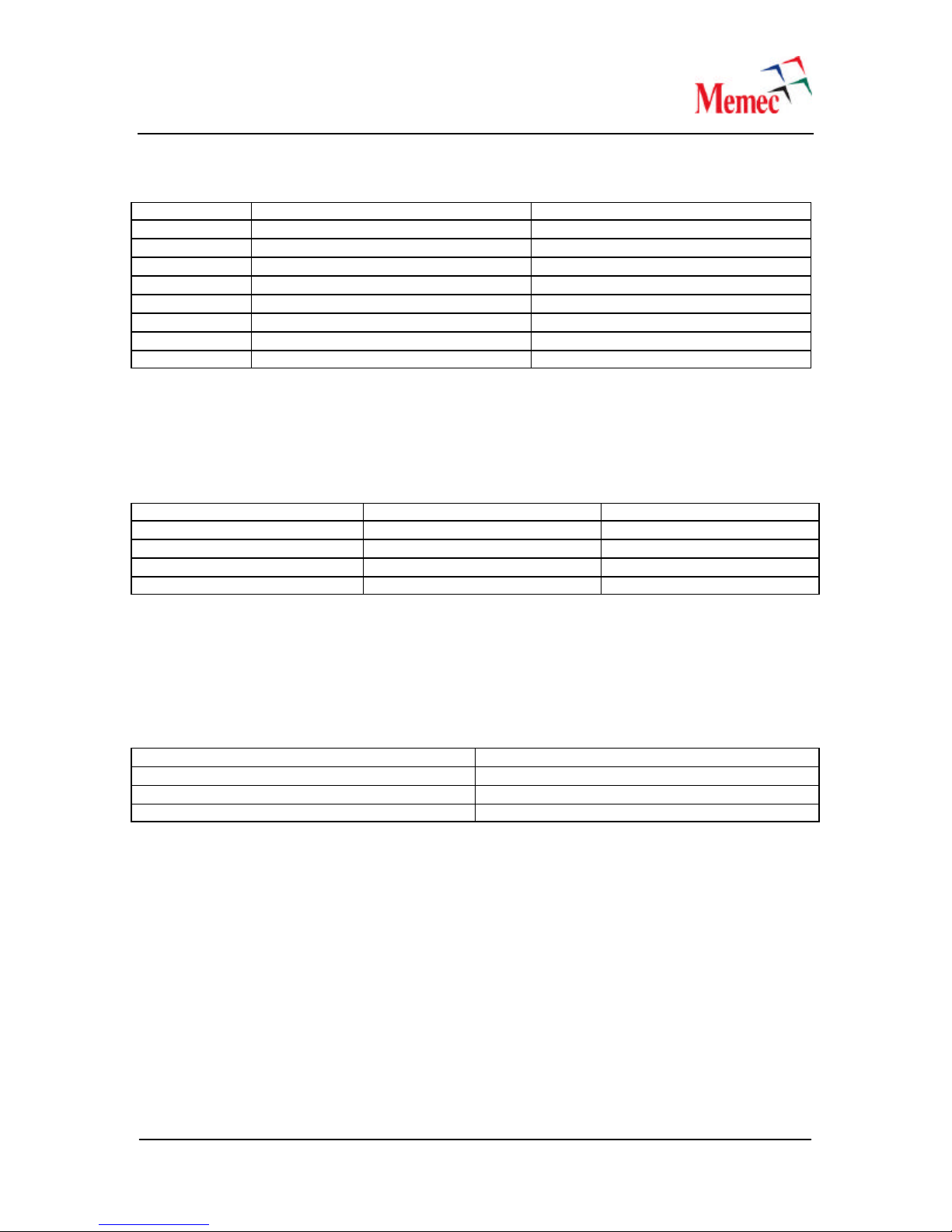
Table 20 – DIP Switch Pin Assignments
Signal Name Description Virtex-4 Pin #
DIP1 User Switch Input 1
DIP2 User Switch Input 2
DIP3 User Switch Input 3
DIP4 User Switch Input 4
DIP5 User Switch Input 5
DIP6 User Switch Input 6
DIP7 User Switch Input 7
DIP8 User Switch Input 8
C10
D10
B6
C6
B4
A4
D2
D1
3.10 User LEDs
The Virtex-4 MB development board provides four user LEDs that can be turned “ON” by driving
the LEDx signal to logic “0”. The following table shows the user LEDs and their associated Virtex4 FPGA pin assignments.
Table 21 – LED Pin Assignments
LED Designation LED # Virtex-4 Pin #
DS9 LED1
DS10 LED2
DS11 LED3
DS12 LED4
N25
V25
L26
K26
3.11 VBAT Jumper
A 3-pin jumper is used to provide user access to the VBAT input of the FPGA. If user is not
sourcing the VBAT voltage, a jumper must be installed on pins 1-2 of the JP27 jumper. User can
source voltage to the VBAT input via pins 2 and 3 of this jumper. The following table shows the
pin assignments for the VBAT jumper.
Table 22 – VBAT Jumper (JP27)
Pin Number Description
1 2.5V
2 VBAT
3 Ground
3.12 Configuration and Debug Ports
Various methods of configuration and debug support are provided on the Virtex -4 MB
development board to assist designers during the testing and debugging of their applications. The
following sections provide brief descriptions of each of these interfaces.
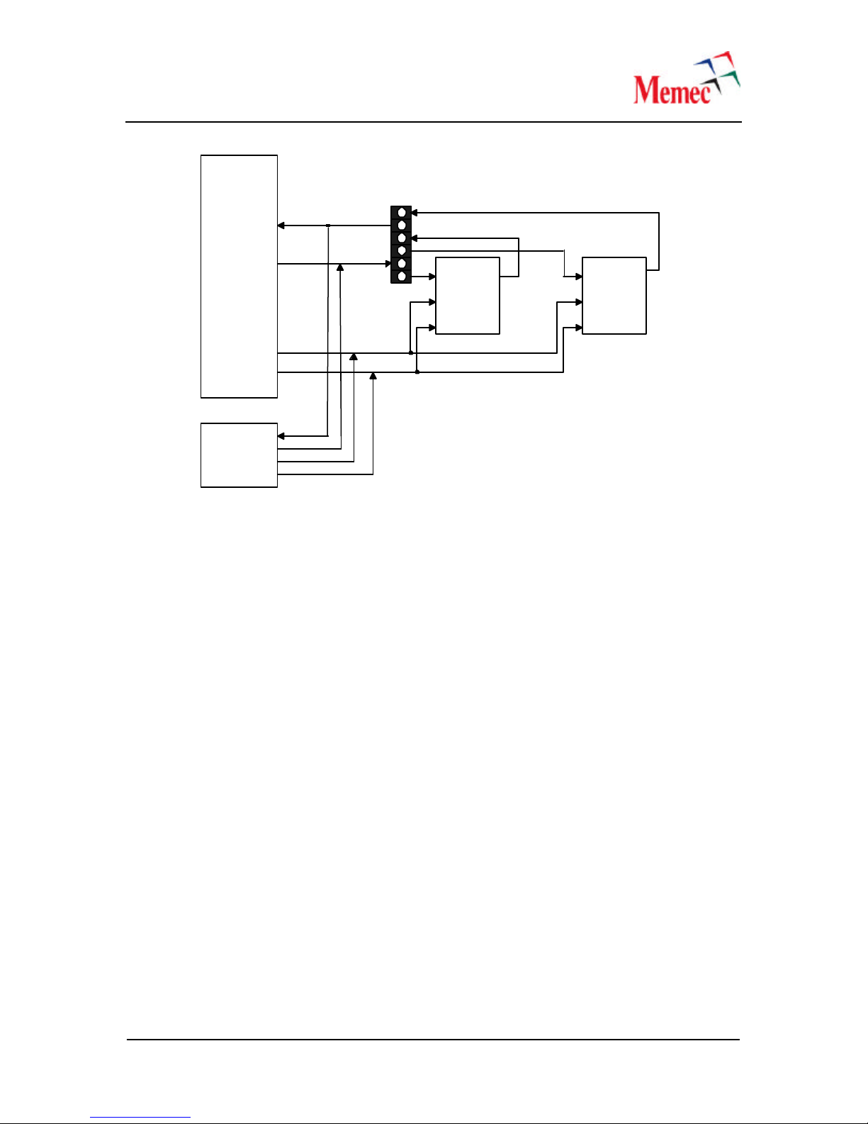
3.12.1 JTAG Chain
The following figure shows the JTAG chain on the Virtex -4 MB development board. The
XC9536XV along with a serial flash is used to configure the FPGA. The serial flash programming
procedure is explained in section 3.11.3.
December 20, 2005 23
Page 27
SAM
Connector
JTAG Port
(PC4)
TDO
TDI
TMS
TCK
JP18
1
3
4
6
2
5
TDI
TMS
TCK
XC9536XV CPLD
TDO TDI
TMS
TCK
Virtex-4 FPGA
TDO
Figure 14 – Vitex-4 MB Development Board JTAG Chain
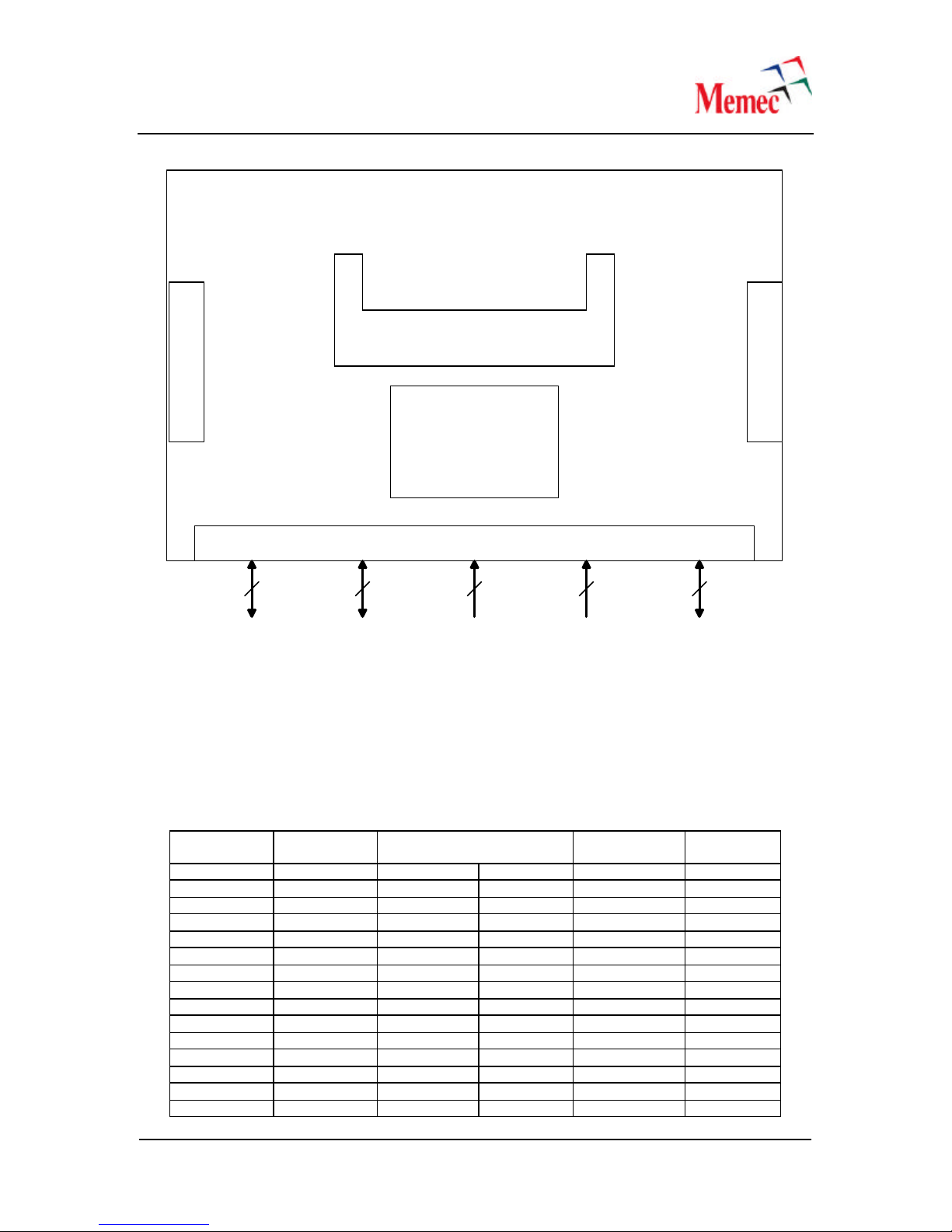
3.12.2 System ACE Module Connector
The Virtex -4 MB development board provides the SAM 50-pin connector on the board for using
the Memec System ACE Module (SAM). The SAM can be used to configure the FPGA or to
provide bulk flash memory to the MicroBlaze processor.
The Virtex-4 MB development board provides a System ACE interface that can be used to
configure the Virtex-4 FPGA. The interface also gives software designers the ability to run realtime operating systems (RTOS) from removable CompactFlash cards . The Memec System ACE
module (DS -KIT-SYSTEMACE) can be used to perform both of these functions. The figure below
shows the System ACE module connected to the header on the Virtex -4 board.
December 20, 2005 24
Page 28
JTAG Test Port
.......
(inludes VCC and GND)
CF Connector
SystemACE™
Controller
.......
stand-alone operation)
JTAG Configuration Port
(includes VCC and GND for
(connects to a 40-pin 0.1" square post header on the main board)
284
JTAG
Configuration Port
MPU
Interface
Figure 15 – SystemACE Module
50-pin Connector
2
Reset &
Clock
10
Power &
Ground
6
Misc
Signals
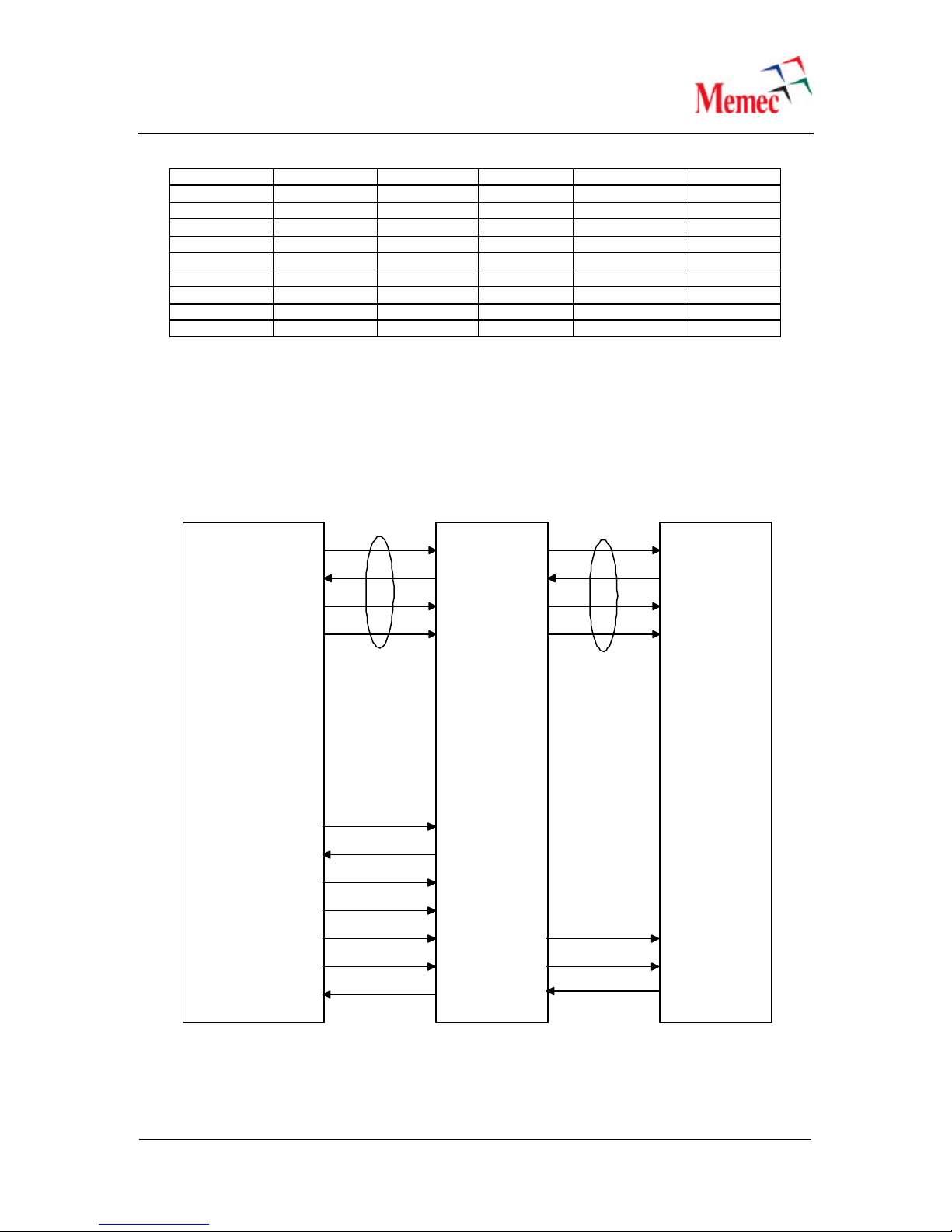
3.12.2.1 System ACE Controller Signal Description
The following table shows the System ACE Module signal assignments to the FPGA I/O pins.
Table 23 - SAM Interface Signals
Virtex-4 Pin # System ACE
Signal Name
3.3V 1 2 3.3V
TDO 3 4 GND
TMS 5 6 CLOCK AE10
TDI 7 8 GND
PROGRAMn 9 10 TCK
GND 11 12 GND
AB7 OEn 13 14 INITn
AB6 MPA0 15 16 WEn V6
Y5 MPA2 17 18 MPA1 AC9
2.5V 19 20 MPA3 AD8
V5 MPD00 21 22 2.5V
AC7 MPD02 23 24 MPD01 AC8
AC6 MPD04 25 26 MPD03 AD6
AF9 MPD06 27 28 MPD05 AB9
AF8 MPD08 29 30 MPD07 AE9
SAM Connector Pin #
(JP16)
System ACE
Signal Name
Virtex-4 Pin
#
December 20, 2005 25
Page 29
AD10 MPD10 31 32 MPD09 AF7
AD11 MPD12 33 34 MPD11 AD12
AE6 MPD14 35 36 MPD13 AE13
W6 MPA4 37 38 MPD15 AA4
AA3 MPA6 39 40 MPA5 Y3
Y4 IRQ 41 42 GND
W3 RESETn 43 44 CEn W5
DONE 45 46 BRDY W4
CCLK 47 48 BITSTREAM
GND 49 50 NC
3.12.3 Serial Data Flash
This section describes the procedure for programming the Atmel serial data flash on the Memec
Virtex-4 MB development board. This serial flash along with a CPLD is used to configure the
Virtex-4 FPGA located on the development board on power up. The following figure shows a
high-level block diagram of the serial flash interface to the Virtex-4 FPGA.
Master Serial
Interface
SPI Interface
CCLK
DIN
INITn
DONE
Virtex-4
FPGA
FPGA_SI
FPGA_SO
FPGA_SCK
FPGA_CSn
FPGA_WPn
FPGA_RESETn
FPGA_RDY/BUSYn
XC9536XV
CPLD
SI
SO
SCK
CSn
Atmel
AT45DB321B
Serial Flash
WPn
RESETn
RDY/BUSYn
Figure 16 – Virtex-4 MB Development Board Configuration Interface
December 20, 2005 26
Page 30
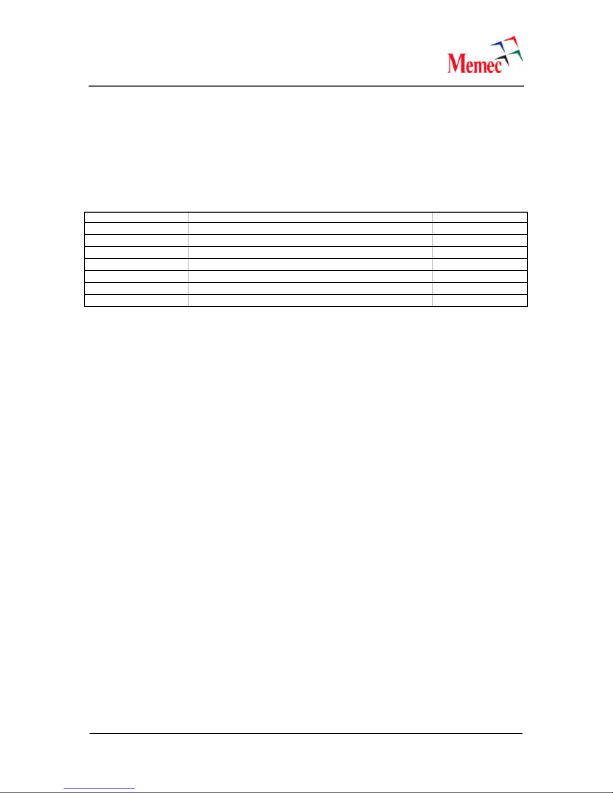
An interface is provided between the FPGA and the CPLD to allow access to the serial flash after
the FPGA has been configured. This interface uses FPGA I/O pins to interface to the serial flash
via the SPI port. The Virtex -4 FPGA uses 8Mb/18.3Mb/14.5Mb (LX25/LX60/SX35) of the serial
flash memory for configuration and this interface allows the rest of the flash to be used for
general-purpose application after the FPGA has been configured. The following table shows the
signals used to implement the interface between the FPGA and the CPLD after the FPGA has
been configured.
Table 24 – FPGA SPI Interface Pin Assignments
Signal Name Description Virtex-4 Pin #
FPGA_SI Serial Flash SPI port data input signal
FPGA_SO Serial Flash SPI port data output signal
FPGA_SCK Serial Flash SPI port clock input signal
FPGA_CSn Serial Flash SPI port chip select input signal
FPGA_WPn Serial Flash SPI port write protect input signal
FPGA_RESETn Serial Flash SPI port reset input signal
FPGA_RDY/BUSYn Serial Flash SPI port ready output signal
R26
T26
P25
U26
U25
M25
V26
The primary function of the CPLD is to translate the Master Serial interface to the SPI interface of
the serial flash. The XC9536XV CPLD uses the FPGA CCLK clock along with the INITn and
DONE signals to drive the SPI SI, SCK and CSn signals. The SO output of the serial flash is used
by the CPLD to drive the DIN signal of the FPGA. For more information on detail of the CPLD
design, please refer to the Xilinx XAPP800.
3.12.3.1 JTAG Chain on the Virtex -4 MB Development Board
The following figure shows the JTAG chain on the Virtex-4 MB development board. As mentioned
in the above section, the CPLD is used for interfacing to the configuration flash and does not
provide any user logic. Hence, this CPLD is programmed by Memec prior to shipping the board.
The programming file for the CPLD is provided in case re-programming of the CPLD becomes
necessary. The CPLD must be programmed prior to performing any operations on the
serial flash such as erasing, programming, reading or verifying.
December 20, 2005 27
Page 31
SAM
Connector
JTAG Port
(PC4)
TDO
TDI
TMS
TCK
JP18
1
3
4
6
2
5
TDI
TMS
TCK
XC9536XV CPLD
TDO TDI
TMS
TCK
Virtex-4 FPGA
TDO
Figure 17 – Virtex-4 MB Development Board JTAG Chain
The following table shows jumper settings for the JTAG chain on the Virtex-4 MB development
board. Since CPLD is already programmed by Memec prior to shipment, the board is shipped
with jumpers installed on pins 1-2 and 4-5 (FPGA only, in the JTAG chain).
Table 25 – JTAG Chain Jumper Settings
Devices in the JTAG Chain JP18 Jumpers Installed
CPLD and FPGA Pins 1-2, 3-4 and 5-6
CPLD Pins 2-3 and 5-6
FPGA Pins 1-2 and 4-5
3.12.3.2 Configuration Flash on the Virtex-4 MB Development Board
The following figure shows the detail interface between the FPGA and the serial flash. A PC4
cable is used to pr ogram the serial flash with the FPGA bitstream. Once the flash is programmed,
the CPLD will read the data from the flash and configure the FPGA over the Master Serial
interface.
December 20, 2005 28
Page 32
JP9
Virtex-4 FPGA
M0
M1
M2
CCLK
DIN
INITn
DONE
XC9536XV
CPLD
JP17
Flash
Programming
Header (PC4)
TDI
TCK
TMS
Atmel
AT45DB321B
Serial Flash
TDO
SI
SO
SCK
CSn
WPn
RESETn
RDY/BUSYn
Flash Programming/
Normal Mode
Jumper
VCC
JP12
Figure 18 – Serial Flash Configuration Interface
3.12.3.3 Procedure for Programming the Serial Flash
1. The Memec Virtex-4 MB development board is shipped with a self-extracting zip file
called Serial_Flash_Programming. Double-click on this self-extracting zip file to unzip it.
After unzipping this file, a folder called C:\Flash_Utilities is created.
2. In order to program the flash, flash programming utilities included in the xapp800 must
be downloaded from the following web site:
http://www.xilinx.com/products/xaw/coolvhdlq.htm
3. Click on the above link to download the xapp800 zip file and unzip it to a temporary
folder on your hard drive. You need to register prior to downloading the xapp800 zip file.
4. Copy xmcsutil.exe and xspi_at.exe files from this temporary folder to the
C:\Flash_Utilities folder. The following table shows the contents of the C: \Flash_Utilities
folder after copying these two executable files.
Table 26 – Files in the Flash_Utilities Folder
File Name Description
December 20, 2005 29
Page 33
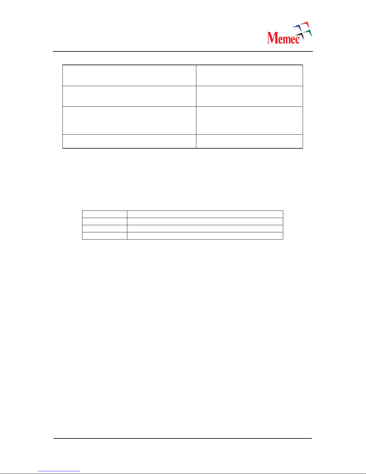
xmcsutil.exe A utility that is used to reverse the
bytes in an MCS file. This is needed
by the xspi_at utility.
xspi_at.exe This utility is used to erase, program
and verify the Atmel serial flash on
the Virtex-4 MB development board.
prog_flash.bat This batch file calls the xmcsutil and
xspi_at utilities to erase, program and
verify the Atmel serial flash on the
Virtex-4 MB development board.
spi_cpld.jed Programming file for the XC9536XV
CPLD
5. Generate a bit file for the FPGA
6. Use iMPACT to generate an MCS file for the bit file generated in the previous step. When
generating the MCS file, select a single platform flash device that will hold the entire
design configuration bits. The following table shows the platform fl ash devices that must
be used when generating the MCS file in iMPACT for the Virtex-4 MB board:
Table 27 – Platform Flash Selection
FPGA Platform Flash Used
LX25 XCF08P, XCF16P or XCF32P
LX60 XCF32P
Sx35 XCF16P or XCF32P
7. Un-install JP9 jumpers.
8. Make sure JP12 jumper is un-installed. When JP12 jumper is un-installed, the CPLD
outputs are placed in the tri-state mode allowing the Flash Programming Header to drive
the serial flash SPI bus.
9. Connect a PC4 cable to the Flash Programming Header (JP17) and power up the Virtex 4 MB development board.
10. Copy the MCS file to the C:\Flash_Utilities folder
11. Open a DOS window in the C:\Flash_Utilities folder and enter the following command to
program the serial flash:
C:\ Flash_Utilities > prog_flash design_name.mcs flash_part_number
Where: design_name.mcs -> The mcs file generated using
the bit file
flash_part_number -> Either AT45DB321B or
AT45DB321C (V4MB board is populated with one or
the other device).
The prog_flash batch file will erase the flash, program and verify it.
December 20, 2005 30
Page 34
12. Once the flash programming is completed, open the verify_result.txt file in the
C:\Flash_Utilities folder. If the flash programming was successful, you should see the
following line in the verify_result.txt file:
--> Total byte mismatches [0]
If there is anything other than this line in the verify_result.txt file, the flash programming
was NOT successful. Check the following jumper settings:
a. Make sure JP9 jumpers are un-installed.
b. Make sure JP12 jumper is un-installed.
After checking these jumper settings go back to the step 11 and re-program the flash.
13. Upon completion of the serial flash programming, power down the board and remove the
PC4 cable from the Flash Programming header.
14. Set the mode jumpers to Master Serial (install all mode jumpers on JP9)
15. Install a jumper on JP12.
16. Power up the board and FPGA will configure.
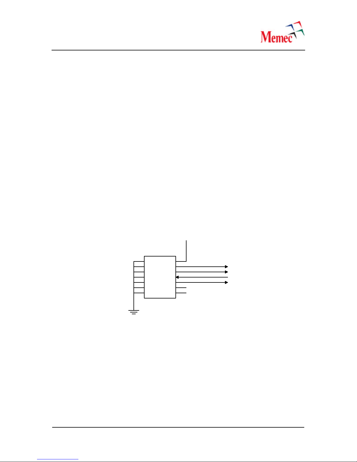
3.12.4 JTAG Port (PC4)
The Virtex-4 MB development board provides a JTAG port (PC4 type) connector for configuration
of the FPGA. The following fig ure shows the pin assignments for the PC4 header on this
development board.
2.5V
PC4
Connector
1 2
3
5
7
9 10
11
13
4
6
8
12
14
Figure 19 – PC4 JTAG Port Connector
3.12.5 Configuration Modes
The following table shows the Virtex-4 configuration modes.
TMS
TCK
TDO
TDI
December 20, 2005 31
Page 35
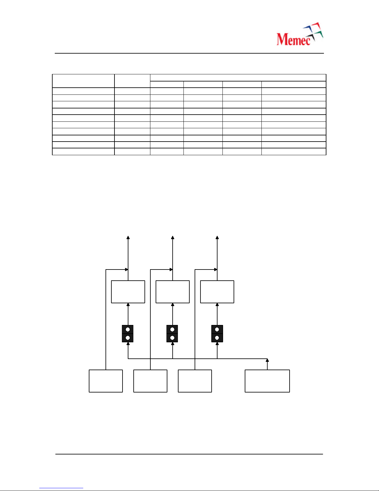
Table 28 - FPGA Configuration Mode Jumper Settings
Configuration Mode Jumpers Mode PC Pull-up
1-2 (M2) 3-4 (M1) 5-6 (M0) 7-8 (HSWAP_EN)
Master Serial Yes Closed Closed Closed Closed
Master Serial No Closed Closed Closed Open
Slave Serial Yes Open Open Open Closed
Slave Serial No Open Open Open Open
Master SelectMap Yes Closed Open Open Closed
Master SelectMap No Closed Open Open Open
Slave SelectMap Yes Open Open Closed Closed
Slave SelectMap No Open Open Closed Open
JTAG Yes Open Closed Open Closed
JTAG No Open Closed Open Open
3.13 Voltage Regulators
The following figure shows the voltage regulators that are used on Virtex-4 MB development
board to provide various on-board voltage sources. As shown in the following figure, a connector
is used to provide the main 5.0V voltage to the board. This voltage source is provided to all onboard regulators to generate the 1.2V, 2.5V, and 3.3V voltages.
3.3V 2.5V 1.2V
3.3V
Connector
3.3V
Regulator
2.5V
Connector
2.5V
Regulator
1.2V
Connector
1.2V
Regulator
5.0V
Connector
Figure 20 - Voltage Regulators
The following table shows the power provided on the development board for the on-board voltage
sources. A 32.5W power adapter (5V @ 6.5A) is used to provide power to the on -board
regulators. The following table shows typical power usage on the Virtex-4 MB development
board.
December 20, 2005 32
Page 36
Table 29 - Power
Voltage Current (A) Power (W) Comments
1.2V 1.5 1.8 FPGA Core voltage
2.5V 2.0 5.0 FPGA I/O voltage, P240 supply voltage
3.3V 3 9.9 FPGA I/O voltage, P240 supply voltage.
Total Power 16.7
For the on-board digital voltages (1.2V, 2.5V, and 3.3V), if the current provided by the on-board
regulator is not sufficient for some applications, the user can directly drive the voltage source and
bypass the on -board regulators.
3.14 Bank I/O Volt age
The following table shows the Virtex-4 bank I/O voltages on the Virtex-4 MB development board.
Table 30 – I/O Bank Voltages
Bank # I/O Voltage
0 2.5V
1 2.5V/3.3V
2 2.5V/3.3V
3 2.5V
4 2.5V
5 2.5V/3.3V
6 2.5V
7 2.5V/3.3V
8 2.5V
9 2.5V
10 3.3V
3.15 P240 Expansion Module Signal Assignments
The following tables show the Virtex -4 pin assignments to the P240 Expansion Module
connectors (JX1 & JX2) located on the Virtex -4 MB development board.
Table 31 – P240 Connector Pin Assignments
Virtex-4 FPGA Pin # I/O Connector
Signal Name JX1 Pin #
5.0V 1 2 5.0V
5.0V 3 4 5.0V
5.0V 5 6 5.0V
5.0V 7 8 5.0V
G17 LIO_SE_42 9 10 LIO_SE_43 H26
G18 LIO_SE_40 11 12 LIO_SE_41 H25
C23 LIO_SE_38 13 14 LIO_SE_39 G26
E22 LIO_SE_36 15 16 LIO_SE_37
H23 LIO_SE_34 17 18 LIO_SE_35
H24 LIO_SE_32 19 20 LIO_SE_33
3.3V 21 22 3.3V
3.3V 23 24 3.3V
3.3V 25 26 3.3V
December 20, 2005 33
I/O Connector
Signal Name
Virtex-4 FPGA Pin #
G25
F26
E26
Page 37
3.3V 27 28 3.3V
G23 LIO_SE_30 29 30 LIO_SE_31
G24 LIO_SE_28 31 32 LIO_SE_29
F23 LIO_SE_26 33 34 LIO_SE_27
F24 LIO_SE_24 35 36 LIO_SE_25
E23 LIO_SE_22 37 38 LIO_SE_23
E24 LIO_SE_20 39 40 LIO_SE_21
D23 LIO_SE_18 41 42 LIO_SE_19
D24 LIO_SE_16 43 44 LIO_SE_17
2.5V 45 46 2.5V
2.5V 47 48 2.5V
2.5V 49 50 2.5V
2.5V 51 52 2.5V
C24 LIO_SE_14 53 54 LIO_SE_15
F16 LIO_SE_12 55 56 LIO_SE_13
F15 LIO_SE_10 57 58 LIO_SE_11
F12 LIO_SE_8 59 60 LIO_SE_9
F13 LIO_SE_6 61 62 LIO_SE_7
D13 LIO_SE_4 63 64 LIO_SE_5
C11 LIO_SE_2 65 66 LIO_SE_3
D11 LIO_SE_0 67 68 LIO_SE_1
GND 69 70 GND
H22 LIO_LVDS_P14 71 72 LIO_LVDS_P15
H21 LIO_LVDS_N14 73 74 LIO_LVDS_N15
GND 75 76 GND
F20 LIO_LVDS_P12 77 78 LIO_LVDS_P13
E20 LIO_LVDS_N12 79 80 LIO_LVDS_N13
G19 LIO_LVDS_P10 81 82 LIO_LVDS_P11
F19 LIO_LVDS_N10 83 84 LIO_LVDS_N11
GND 85 86 GND
H20 LIO_LVDS_P8 87 88 LIO_LVDS_P9
G20 LIO_LVDS_N8 89 90 LIO_LVDS_N9
GND 91 92 GND
D22 LIO_LVDS_P6 93 94 LIO_LVDS_P7
C22 LIO_LVDS_N6 95 96 LIO_LVDS_N7
GND 97 98 GND
C20 LIO_LVDS_P4 99 100 LIO_LVDS_P5
B20 LIO_LVDS_N4 101 102 LIO_LVDS_N5
GND 103 104 GND
C19 LIO_LVDS_P2 105 106 LIO_LVDS_P3
D18 LIO_LVDS_N2 107 108 LIO_LVDS_N3
GND 109 110 GND
C17 LIO_LVDS_P0 111 112 LIO_LVDS_P1
D17 LIO_LVDS_N0 113 114 LIO_LVDS_N1
GND 115 116 GND
B17 LIO_CLKIN_P 117 118 LIO_CLKIN_1
A17 LIO_CLKIN_N 119 120 LIO_CLKIN_0
GND 121 122 GND
GND 123 124 GND
GND 125 126 GND
E25
D26
D25
C26
C25
B24
A24
B23
A23
F11
C16
D16
D15
D14
E14
F14
C21
B21
F18
E18
E21
D21
D20
D19
E17
F17
A22
A21
A20
A19
B18
A18
E13
D12
December 20, 2005 34
Page 38
GND 127 128 GND
GND 129 130 GND
GND 131 132 GND
Table 32– P240 Connector Pin Assignments
Virtex-4 FPGA Pin # I/O Connector
Signal Name JX2 Pin #
5.0V 1 2 5.0V
5.0V 3 4 5.0V
5.0V 5 6 5.0V
5.0V 7 8 5.0V
W26 RIO_SE_42 9 10 RIO_SE_43 W23
W25 RIO_SE_40 11 12 RIO_SE_41 W24
Y26 RIO_SE_38 13 14 RIO_SE_39 Y23
Y25 RIO_SE_36 15 16 RIO_SE_37
AA26 RIO_SE_34 17 18 RIO_SE_35
AB26 RIO_SE_32 19 20 RIO_SE_33
3.3V 21 22 3.3V
3.3V 23 24 3.3V
3.3V 25 26 3.3V
3.3V 27 28 3.3V
AB25 RIO_SE_30 29 30 RIO_SE_31
AC26 RIO_SE_28 31 32 RIO_SE_29
AC25 RIO_SE_26 33 34 RIO_SE_27
V20 RIO_SE_24 35 36 RIO_SE_25
AD26 RIO_SE_22 37 38 RIO_SE_23
W20 RIO_SE_20 39 40 RIO_SE_21
AD25 RIO_SE_18 41 42 RIO_SE_19
AD19 RIO_SE_16 43 44 RIO_SE_17
2.5V 45 46 2.5V
2.5V 47 48 2.5V
2.5V 49 50 2.5V
2.5V 51 52 2.5V
AA16 RIO_SE_14 53 54 RIO_SE_15
AA15 RIO_SE_12 55 56 RIO_SE_13
AB14 RIO_SE_10 57 58 RIO_SE_11
AA14 RIO_SE_8 59 60 RIO_SE_9
AB13 RIO_SE_6 61 62 RIO_SE_7
AA13 RIO_SE_4 63 64 RIO_SE_5
AA12 RIO_SE_2 65 66 RIO_SE_3
AA11 RIO_SE_0 67 68 RIO_SE_1
GND 69 70 GND
Y20 RIO_LVDS_P14 71 72 RIO_LVDS_P15
Y21 RIO_LVDS_N14 73 74 RIO_LVDS_N15
GND 75 76 GND
AA19 RIO_LVDS_P12 77 78 RIO_LVDS_P13
AA20 RIO_LVDS_N12 79 80 RIO_LVDS_N13
AA18 RIO_LVDS_P10 81 82 RIO_LVDS_P11
Y18 RIO_LVDS_N10 83 84 RIO_LVDS_N11
GND 85 86 GND
I/O Connector
Signal Name
Virtex-4 FPGA Pin #
Y24
AA23
AA24
AB23
AB24
AB21
W22
Y22
W21
AC21
AC19
AC16
AC15
AC14
AD14
AC13
AD13
AC12
AC11
V21
V22
AC23
AC24
AC22
AB22
December 20, 2005 35
Page 39
AF24 RIO_LVDS_P8 87 88 RIO_LVDS_P9
AE24 RIO_LVDS_N8 89 90 RIO_LVDS_N9
GND 91 92 GND
AF23 RIO_LVDS_P6 93 94 RIO_LVDS_P7
AE23 RIO_LVDS_N6 95 96 RIO_LVDS_N7
GND 97 98 GND
AF21 RIO_LVDS_P4 99 100 RIO_LVDS_P5
AF22 RIO_LVDS_N4 101 102 RIO_LVDS_N5
GND 103 104 GND
AF19 RIO_LVDS_P2 105 106 RIO_LVDS_P3
AF20 RIO_LVDS_N2 107 108 RIO_LVDS_N3
GND 109 110 GND
AF18 RIO_LVDS_P0 111 112 RIO_LVDS_P1
AE18 RIO_LVDS_N0 113 114 RIO_LVDS_N1
GND 115 116 GND
Y17 RIO_CLKOUT_P 117 118 RIO_CLKOUT_1
AA17 RIO_CLKOUT_N 119 120 RIO_CLKOUT_0
GND 121 122 GND
GND 123 124 GND
GND 125 126 GND
GND 127 128 GND
GND 129 130 GND
GND 131 132 GND
AB20
AC20
AD22
AD23
AE21
AD21
AC18
AB18
Y19
W19
U7
U6
4 Revisions
V3.0 Initial release for Rev 3 board Dec 20, 2005
December 20, 2005 36
Page 40
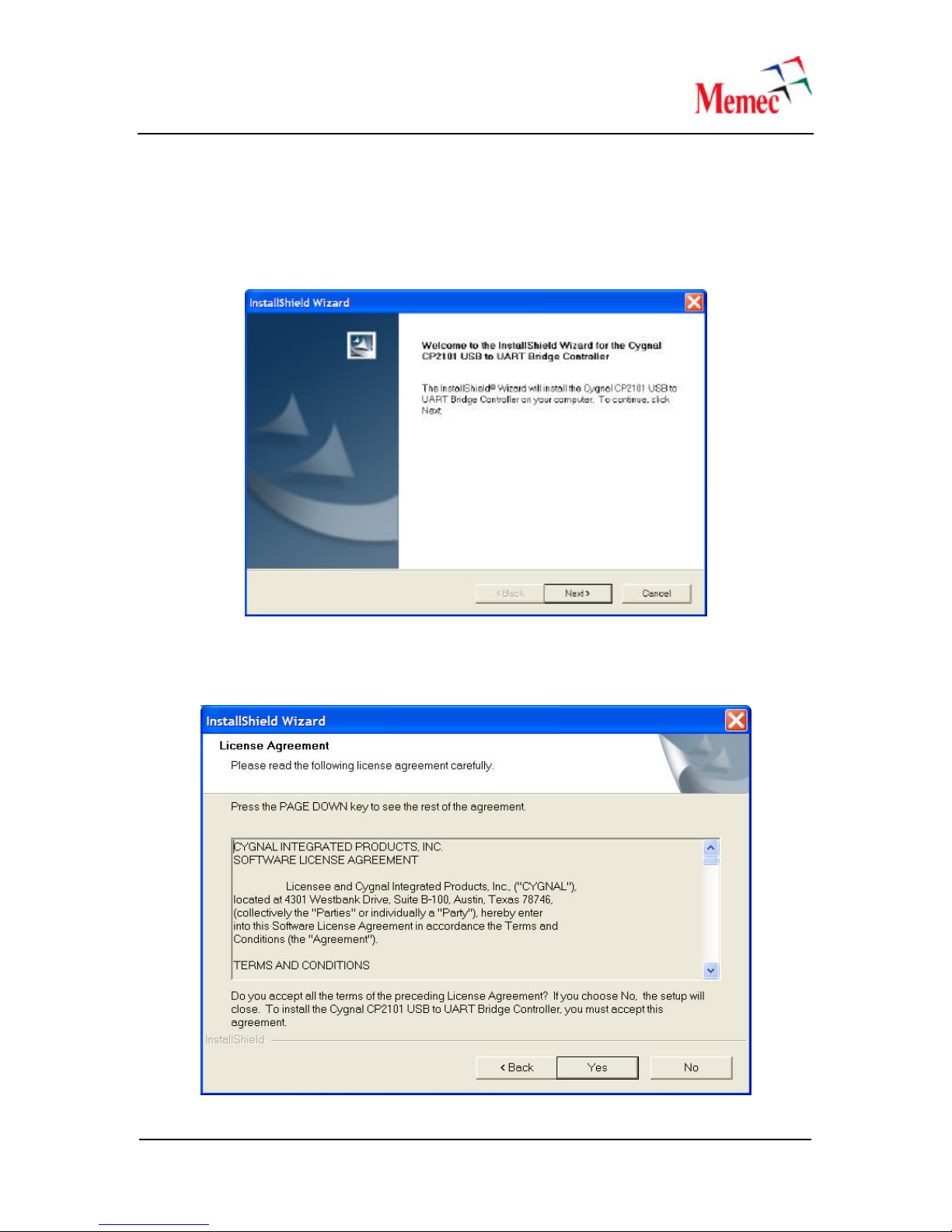
Appendix A
1. Double-click CP2101_Drivers.exe.
Launching CP2101 Driver Installation
2. Click Next.
3. Read the license agreement and then click Yes.
December 20, 2005 37
Cygnal License Agreement
Page 41
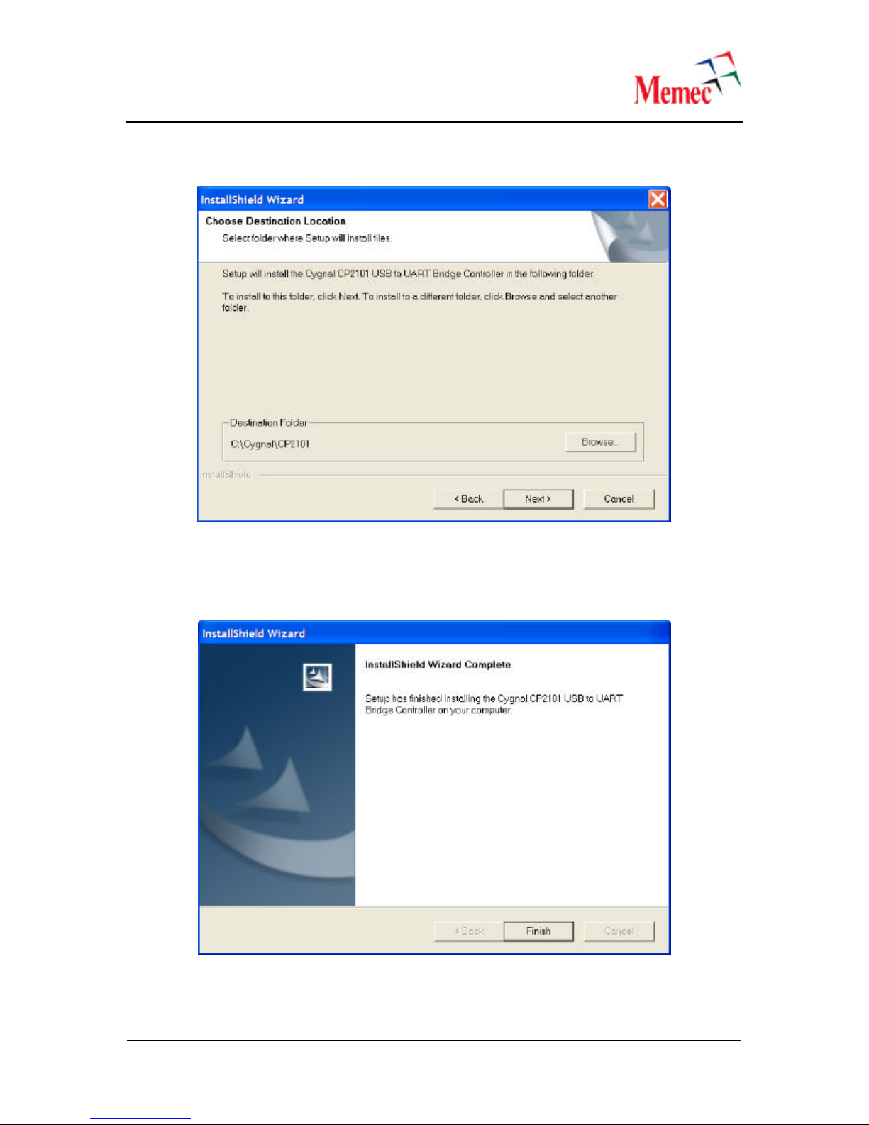
4. Browse to an acceptable installation directory, and then click Next.
CP2101 Destination Location
5. The drivers are extracted to the selected directory. Click Finish once the extraction
completes.
6. To finish the installation, plug the USB cable into the board and a USB port on the PC.
December 20, 2005 38
CP2101 Installation Successful
Page 42
7. Turn the board power switch to the ON position.
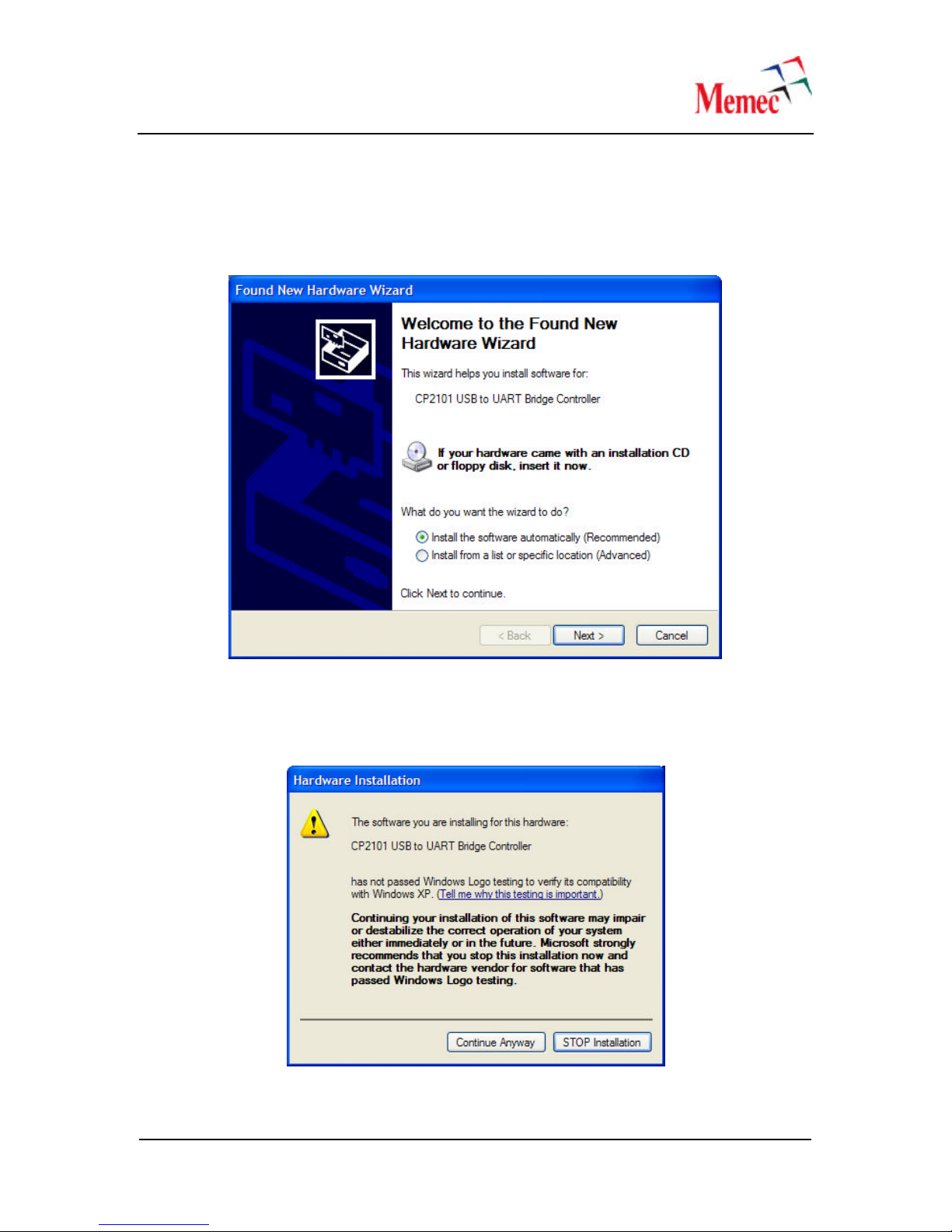
8. The Found New Hardware Wizard launches. Click the radio button to Install the
software automatically (Recommended) and then click Next.
Found New Hardware Wizard
9. The driver installation begins . If installing on WindowsXP, a warning is received stating
that Windows Logo testing has not passed, as shown below. Click Continue Anyway.
Windows Logo Testing Not Passed
December 20, 2005 39
Page 43
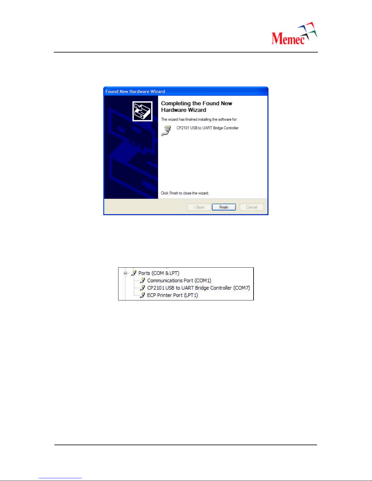
10. The driver installation completes at this point. Click Finish in the Found New Hardware
Wizard.
CP2101 Driver Installation Complete
11. Open the Device Manager (Control Panel à System à Hardware tab à Device
Manager).
12. Under the Ports heading, a new device shows up, called CP2101 USB to UART Bridge
Controller.
CP2101 Recognized as COM Port
13. If the CP2101 does not show up under ports, it may show up under “Other Devices” with
a yellow exclamation mark. In this case, unplug the USB cable, run the setup manually
(C:\Cygnal\CP2101\WIN\Setup.exe), and then plug the USB cable back in.
14. The O/S automatically assigns a COM Port number, typically between COM3 and COM7.
For consistency, the COM number will be manually changed. Right click on CP2101
USB to UART Bridge Controller and select Properties.
December 20, 2005 40
Page 44
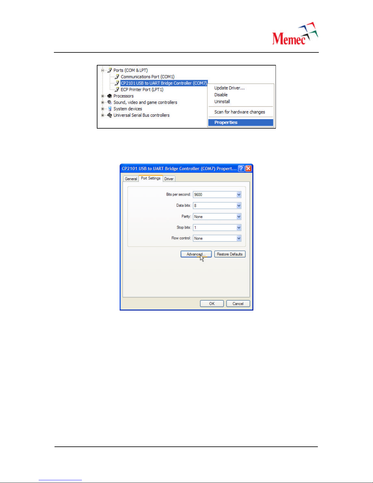
COM Port Properties
15. Change to the Port Settings tab and select Advanced.
16. Select COM10 in the COM Port Number field, and then click OK twice.
December 20, 2005 41
Port Settings – Advanced
Page 45
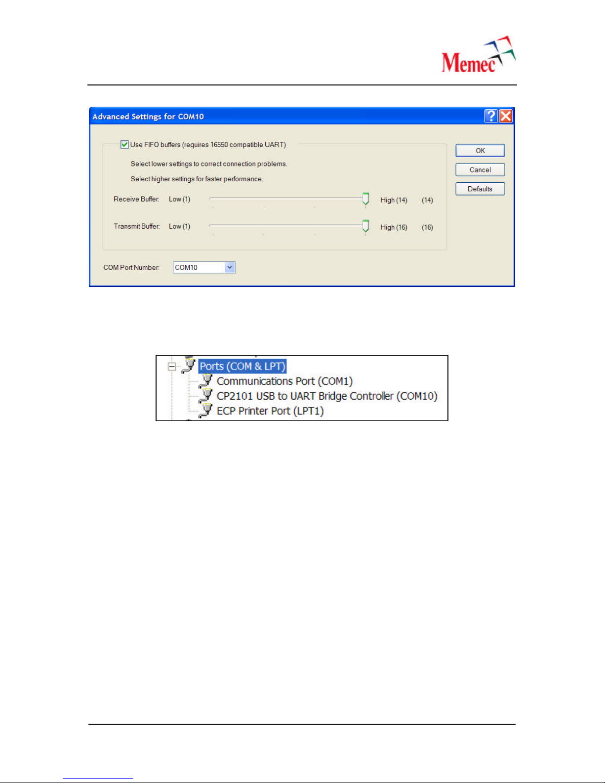
Changing the COM Port Number
17. Close the Device Manager, and then re-open it. Under Ports, the CP2101 USB to UART
Bridge Controller is now assigned to COM10, as shown below.
CP2101 Assigned to COM10
December 20, 2005 42
 Loading...