

MELEXIS US5781E, US5781L Datasheet
US5781
CMOS High Sensitivity Switch
Preliminary Datasheet
Features and Benefits
• Chopper stabilized amplifier stage
• New miniature package / thin, high reliability package
• Operation down to 3.5V
• CMOS for optimum stability, quality, and cost
Applications
• Solid state switch
• Limit switch
• Current limit
• Interrupter
Ordering Information
Part No. Temperature Suffix Package Temperature Range
US5781 E SO or UA -40°C to 85°C Extended
US5781 L SO or UA -40°C to 150°C Automotive
Preliminary
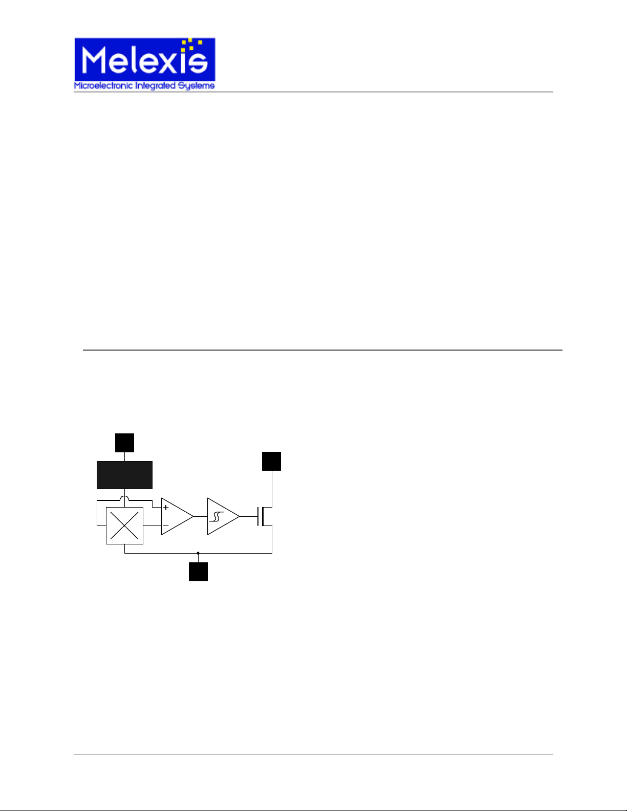
Functional Diagram
SO Package
Pin 1 - V
DD
Pin 2 - Output
Pin 3 - GND
Output
V
DD
Voltage
Regulator
Chopper
GND
UA Package
Pin 1 - V
DD
Pin 2 - GND
Pin 3 - Output
Note: This is a static-sensitive device; please observe ESD precautions. Reverse VDD protection is not included. For reverse voltage
protection, a 100Ω resistor in series with VDD is recommended.
Description
The US5781 is a unipolar Hall effect sensor IC fabricated from mixed signal CMOS technology. It incorporates advanced chopper stabilization techniques to provide accurate and stable magnetic
switch points. There are many applications for this
sensor in addition to those listed above. The design, specifications and performance have been
optimized for applications of solid state switches.
The output transistor will be switched on (BOP) in
the presence of a sufficiently strong South pole
magnetic field facing the marked side of the package. Similarly, the output will be switched off (BRP)
in the presence of a weaker South field and remain
off with “0” field. The SOT-23 device is reversed
from the UA package. The SOT-23 output transistor will be switched on (BOP) in the presence of a
sufficiently strong North pole magnetic field subjected to the marked face.
US5781 CMOS High Sensitivity Switch 3901005781 Rev 1.7 7/23/01 Page 1
US5781
CMOS High Sensitivity Switch
Preliminary Datasheet
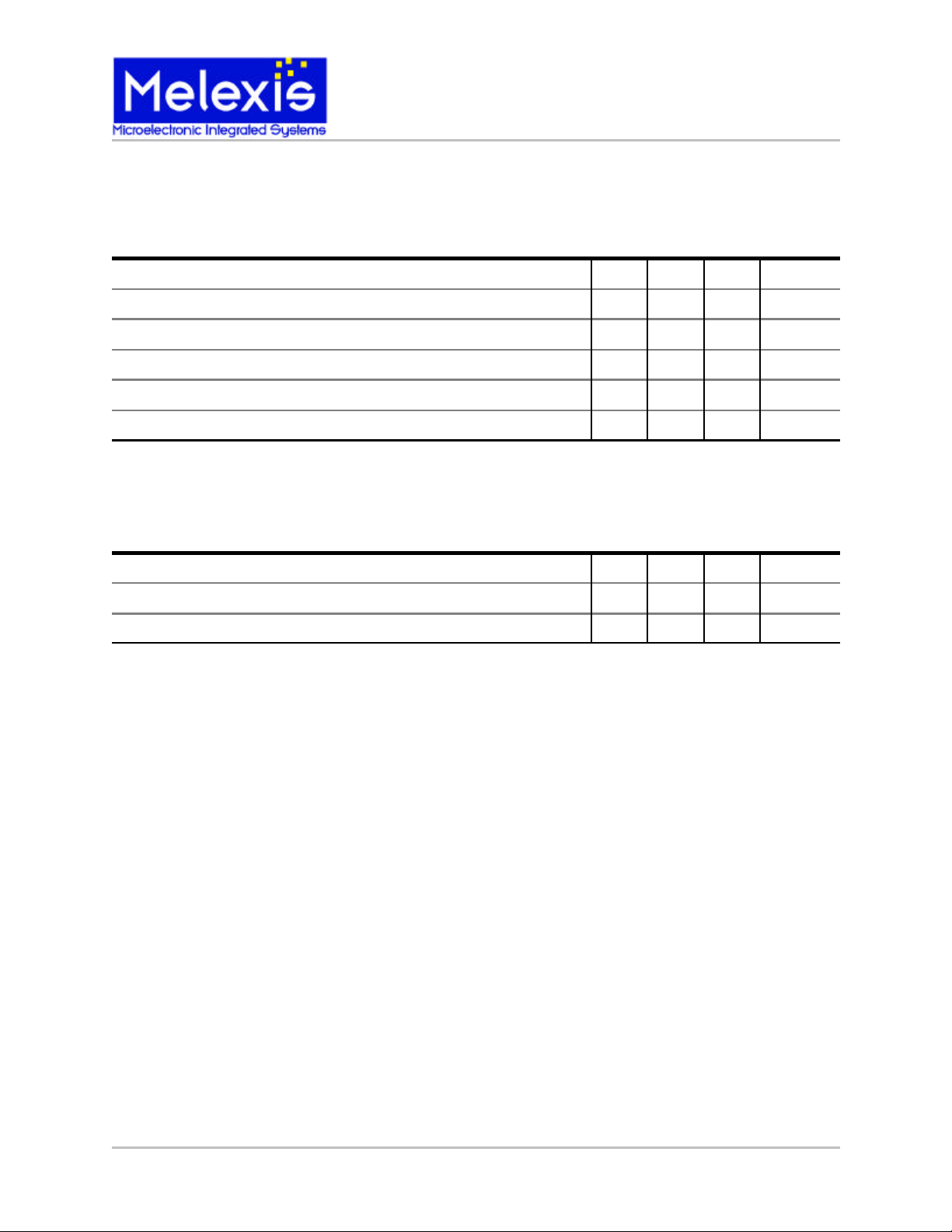
US5781 Electrical Specifications
DC operating parameters: TA = -40 to 150oC, VDD = 12VDC (unless otherwise specified).
Parameter Symbol Test Conditions Min Typ Max Units
Supply Voltage VDD Operating 3.5 24 V
Supply Current IDD B<BRP 0.5 2.5 5.0 mA
Saturation Voltage V
Output Leakage I
Output Rise Time tr VDD = 12V, RL = 1.1KÙ, CL = 20pf 0.04 ì s
Output Fall Time tf VDD = 12V, RL = 1.1KÙ, CL = 20pf 0.18 ì s
I
DS(on)
B<BRP, V
OFF
OUT
= 20 mA, B>BOP 0.3 0.5 V
= 27V 0.01 5.0 ì A
OUT
US5781 Magnetic Specifications
Magnetic operating parameters: TA = -40 to 150oC, VDD =12 VDC (unless otherwise specified).
Parameter Symbol Test Conditions Min Typ Max Units
Operating Point BOP 7.0 12.0 15.0 mT
Release Point BRP 3.5 7.0 10.0 mT
Hysteresis B
Note: 1 mT = 10 Gauss.
2.0 5.0 7.0 mT
hys
Melexis Inc. reserves the right to make changes without further notice to any products herein to improve reliability, function or design. Melexis does
not assume any liability arising from the use of any product or application of any product or circuit described herein.
US5781 CMOS High Sensitivity Switch 3901005781 Rev 1.7 7/23/01 Page 2
 Loading...