

MELEXIS US2882L, US2882E, US2881L, US2881E Datasheet
US2881/2882
CMOS High Sensitivity Latch
US2881 CMOS High Sensitivity Latch 3901002881 Rev 5.6 23/July/00 Page 1
Description
The design specifications and performance of the
Melexis US2881 have been optimized for commutation applications in brushless DC motors and
automotive speed sensing.
The output transistor will be latched on (BOP) in the
presence of a sufficiently strong South pole magnetic field facing the marked side of the package.
Similarly, the output will be latched off (BRP) in the
presence of a North field. The SOT-23 device is
reversed from the UA package. The SOT-23 output
transistor will be latched on (BOP) in the presence
of a sufficiently strong North pole magnetic field
subjected to the marked face.
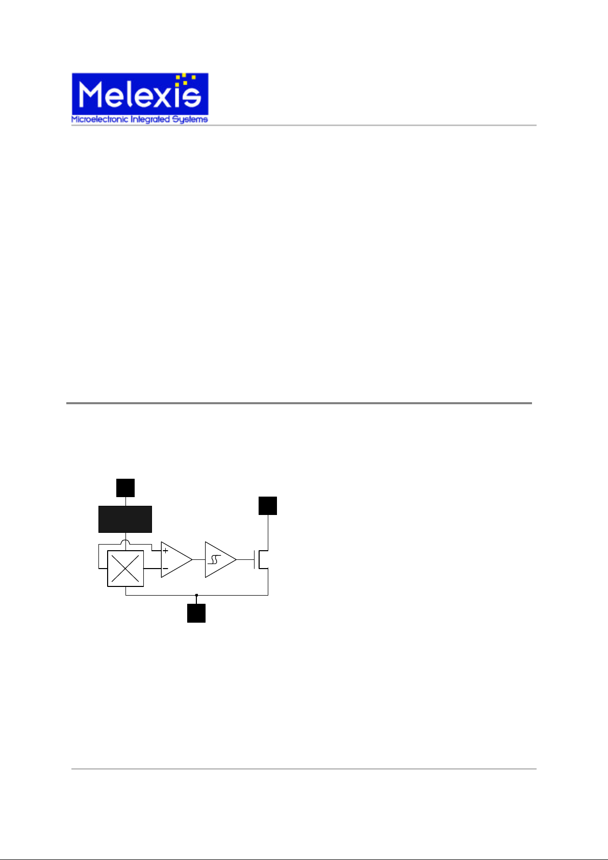
Functional Diagram
Note: Static sensitive device; please observe ESD precautions. Reverse V
DD
protection is not included. For reverse voltage protection,
a 100
Ω
resistor in series with VDD is recommended.
Output
GND
V
DD
Voltage
Regulator
Chopper
SO Package
Pin 1 - V
DD
Pin 2 - Output
Pin 3 - GND
UA Package
Pin 1 - V
DD
Pin 2 - GND
Pin 3 - Output
Features and Benefits
• Chopper stabilized amplifier stage
• Optimized for BDC motor applications
• New miniature package / thin, high reliability package
• Operation down to 3.5V
• CMOS for optimum stability, quality, and cost
• Ultra low I
DD
current
Applications
• Solid state switch
• Brushless DC motor commutation
• Speed sensing
• Linear position sensing
• Angular position sensing
• Current sensing
Ordering Information
Part No. Temperature Suffix Package Temperature Range
US2881 / US2882 E SO or UA -40oC to 85oC Extended
US2881 / US2882 L SO or UA -40oC to 150oC Full Temp.
*Contact Factory or Sales Representative for Legacy Temperature Versions
US2881 CMOS High Sensitivity Latch 3901002881 Rev 5.6 23/July/00 Page 2
US2881/2882
CMOS High Sensitivity Latch
US2881 and US2882 Electrical Specifications
DC operating parameters: TA = 25oC, VDD = 12VDC (unless otherwise specified).
Parameter
Symbol Test Conditions Min Typ Max Units
Supply Voltage VDD Operating 3.5 27 V
Supply Current IDD B<BOP 1.5 2.0 4.0 mA
Saturation Voltage V
DS(on)
I
OUT
= 20 mA, B>BOP 0.4 0.5 V
Output Leakage I
OFF
B<BRP, V
OUT
= 27V 0.01 5.0 ì A
Output Rise Time tr VDD = 12V, RL = 1.1KÙ, CL = 20pf 0.04 ì s
Output Fall Time tf VDD = 12V, RL = 1.1KÙ, CL = 20pf 0.18 ì s
US2881 Magnetic Specifications
Parameter Symbol Test Conditions Min Typ Max Units
Operating Point BOP 0.5 2.0 4.5 mT
Release Point BRP -4.5 -2.0 -0.5 mT
Hysteresis B
hys
3.0 4.0 5.0 mT
US2882 Magnetic Specifications
Parameter Symbol Test Conditions Min Typ Max Units
Operating Point BOP -2.0 2.0 6.0 mT
Release Point BRP -6.0 -2.0 2.0 mT
Hysteresis B
hys
3.0 4.0 5.0 mT
Melexis Inc. reserves the right to make changes without further notice to any products herein to improve reliability, function or design.
Melexis does not assume any liability arising from the use of any
product or application of any product or circuit described herein.
Note: 1 mT = 10 Gauss.
Supply Voltage (Operating), VDD 24V
Supply Current (Fault), IDD 50mA
Output Voltage, V
OUT
24V
Output Current (Fault), I
OUT
50mA
Power Dissipation, PD 100mW
Operating Temperature Range, TA -40 to 150°C
Storage Temperature Range, TS -65 to 150°C
Maximum Junction Temp, TJ 175°C
ESD Sensitivity (All Pins) +/- 4KV
Absolute Maximum Ratings
US2881/2882
CMOS High Sensitivity Latch
US2881 CMOS High Sensitivity Latch 3901002881 Rev 5.6 23/July/00 Page 3
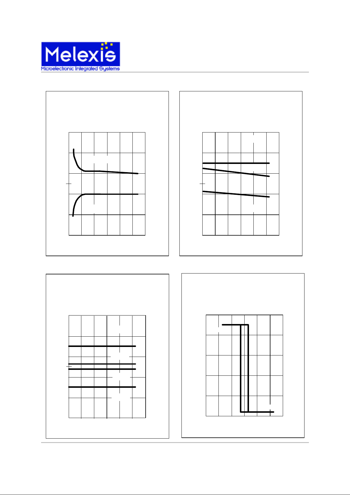
Performance Graphs
12.5
Flux Density (mT)
Supply Voltage (V)
Typical Magnetic Switch Points
versus
Supply Voltage
2881
15
-7.5
-2.5
2.5
7.5
1050 20 25 30
B
OP
B
RP
-12.5
12
-12.5
Flux Density (mT)
Temperature (oC)
Typical Magnetic Switch Points
versus
Temperature
2881
80
-7.5
-2.5
2.5
7.5
0-40 120 160 20040
B
OP
B
HYS
B
RP
30
Output Voltage (V)
Flux Density (mT)
Output Voltage
versus
Flux Density
2881
0
6
12
18
24
-10-20-30 10 20 30
0
V
DD
V
out
B
OP
B
RP
12.5
-12.5
Flux Density (mT)
Temperature (oC)
Min/Max Magnetic Switch
Range
versus
Temperature
2881
80
-7.5
-2.5
2.5
7.5
0-40 120 160 20040
B
OP
Max
B
OP
Min
B
RP
Min
B
RP
Max
 Loading...