

MELEXIS US1881L, US1881E Datasheet
US1881
CMOS Multi-Purpose Latch
Features and Benefits
• Chopper stabilized amplifier stage
• Optimized for BDC motor applications
• New miniature package / thin, high reliability package
• Operation down to 3.5V
• CMOS for optimum stability, quality and cost
Applications
• Solid state switch
• Brushless DC motor commutation
• Speed sensing
• Linear position sensing
• Angular position sensing
• Current sensing
Ordering Information
Part No. Temperature Suffix Package Temperature Range
US1881 E SO or UA -40oC to 85oC Commercial
US1881 L SO or UA -40oC to 150oC Automotive
*Contact factory or sales representative for legacy temperature options
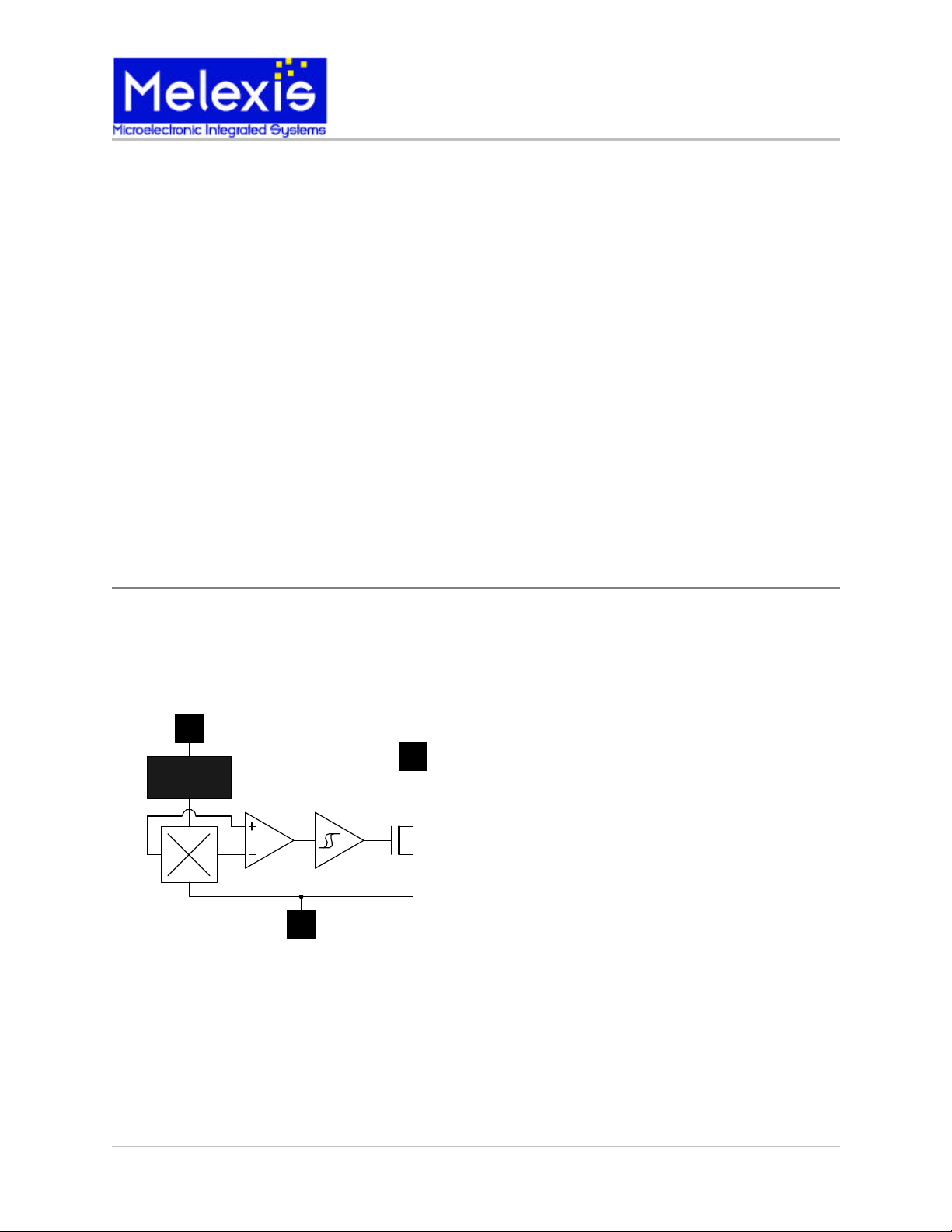
Functional Diagram
SO Package
Pin 1 - V
DD
Pin 2 - Output
Pin 3 - GND
Output
V
DD
Voltage
Regulator
Chopper
GND
UA Package
Pin 1 - V
DD
Pin 2 - GND
Pin 3 - Output
Note: Static sensitive device; please observe ESD precautions. Reverse VDD protection is not included. For reverse voltage protection, a 100Ω resistor in series with VDD is recommended.
Description
The US1881 is the industry’s first Hall integrated
circuit in a SOT-23 package. The US1881 is a bipolar Hall effect sensor IC fabricated from mixed
signal CMOS technology. It incorporates advanced
chopper stabilization techniques to provide accurate and stable magnetic switch points. There are
many applications for this HED in addition to those
listed above. The design, specifications and performance have been optimized for commutation
applications in 5V and 12V brushless DC motors.
The output transistor will be latched on (BOP) in the
presence of a sufficiently strong South pole magnetic field facing the marked side of the package.
Similarly, the output will be latched off (BRP) in the
presence of a North field.
The SOT-23 device is reversed from the UA package. The SOT-23 output transistor will be latched
on in the presence of a sufficiently strong North
pole magnetic field applied to the marked face.
US1881 CMOS Multi-Purpose Latch 3901001881 Rev. 5.2 7/23/01 Page 1
US1881
CMOS Multi-Purpose Latch
US1881 Electrical Specifications
DC Operating Parameters: TA = 25, VDD = 12VDC (unless otherwise specified).
Parameter Symbol Test Conditions Min Typ Max Units
Supply Voltage VDD Operating 3.5 24 V
Supply Current IDD B<BOP 1.5 2.5 4.0 mA
Saturation Voltage V
Output Leakage I
I
DS(on)
B<BRP, V
OFF
OUT
= 20 mA, B>BOP 0.4 0.5 V
= 20V 0.01 5.0 ì A
OUT
Output Rise Time tr VDD = 12V, RL = 1.1KÙ, CL = 20pf 0.04 ì s
Output Fall Time tf VDD = 12V, RL = 1.1KÙ, CL = 20pf 0.18 ì s
Parameter Symbol Test Conditions Min Typ Max Units
Operating Point BOP 1.0 5.0 9.0 mT
Release Point BRP -9.0 -5.0 -1.0 mT
Hysteresis B
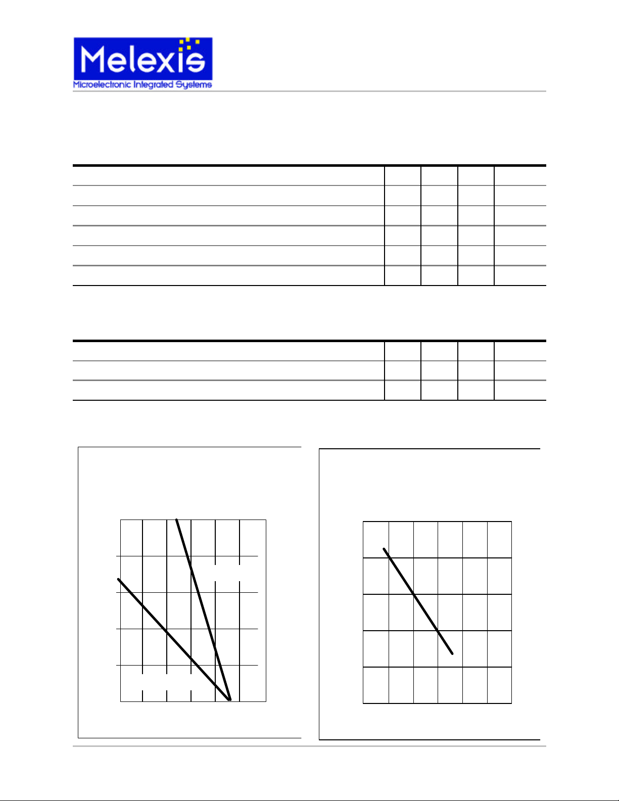
Performance Graphs
Power Dissipation
versus
Temperature
5.5 10.0 12.0 mT
hys
Wave Soldering Parameters
500
400
300
200
All Devices
UA Package
R
=206oC/W
θJA
280
260
C)
o
240
220
All Devices
Solder Temperature (
100
Package Power Dissipation (mW)
0
SO Package
R
θ
JA
0-40 120 160 20040
=575oC/W
80
Temperature (oC)
US1881 CMOS Multi-Purpose Latch 3901001881 Rev. 5.2 7/23/01 Page 2
200
1050 20 25 30
Time in Wave Solder (Seconds)
15
 Loading...