

MELEXIS TH8082JDC Datasheet

Features and Benefits
TH8082
Single LIN Bus
Transceiver
www.melexis.com
Page 1 Data Sheet Rev 1.0 June 2001
Single wire LIN transceiver
Compatibl e to LIN Protoc ol S pec ification, Rev. 1.1
Compatible to ISO9141 functions
Control Output for voltage regulator
Up to 20 kbps bus speed
Low RFI due to slew rate contr ol
Fully integrated receiver filter
Protection against load dump, jump start
Bus terminals proof against short-cir c uits and transients in the
automotiv e environment
Very low (25 µA) typical power consum ption in sleep mode
Thermal ov erl oad and short ci r c uit pr otection
High impendance Bus pin in case of loss of ground and undervoltage c ondition
± 4kV ESD protecti on on bus pin
Ordering Information
Part No. Temperature Rang e Package
TH8082 JDC -40ºC...125ºC SOIC8, 150mil
General Descri ption
The TH8082 is a physical layer device for a single wire
data link capable of operating in applications where high
data rate is not required and a lower data rate can
achieve cost reductions in both the physical media components and in the microprocessor which use the network. The TH8082 is designed in accordance to the
physical layer definition of the LIN Protocol Specification , Rev. 1.2 . The IC furthermore can be used in
ISO9141 systems.
TH8082
1
2
3
4
8
7
6
5
RxD
GNDTxD
EN
INH
VS
BUSVCC
Pin Diagram
SOIC8NB
Because of the very low current consumption of the
TH8082 in the recessive state it’s particularly suitable for
ECU applications with hard standby current requirement s .
An advanced sleep mode capability allows
a shutdown of the whole appli cation . The incl uded
wake-up function detects incoming dominant bus
messages and enables the v oltage regulator.

TH8082
Single LIN Transceiver
www.melexis.com
Page 2 Data Sheet Rev 1.0 June 2001
Functional Diagram
SLEW RATE
BUS Driver
Biasing &
Bandgap
VS
internal Supply
&
References
Receive
Comparator
Input
Filter
TH8082
Thermal
Protection
BUS
GND
POR
MODE
CONTROL
TxD
RxD
VCC
EN
INH
Wake-up
Filter
Figure 1 - Block Diagram
TH8082
Single LIN Transceiver
www.melexis.com
Page 3 Data Sheet Rev 1.0 June 2001
Functional Description
After power on the chip automatically enters the V
BAT
-
stanby mode . In this intermediate mode the INH output
will becom e HIGH (V
S
) and therefore the voltage regula-
tor will provi de the V
CC
- supply . The transceiver will
remain the V
BAT
-stanby mode until the controller sets it to
normal operation ( EN = High ) . Only in this mode bus
communication is possible. The TH8082 switches itself in
the V
BAT
-stanby mode if V
CC
is missing or below the
threshold.
The sleep mode ( EN = LOW) can only be reached from
normal mode and permits a very low power consumtion
because the transceiver and even the external voltage
regulator get disabled. If the V
CC
has been s witch ed of f a
wake-up request from the bus line will cause the TH8082
to enter the V
BAT
-stanby mode (VCC is present again) and
sets the RxD output to low until the device enters the
normal operation mode (active LOW interrupt at RxD). If
the INH pin is not connect ed to th e regulator or the inh ibitabl e extern al regu lator i s not the on e that pr ovides t he
V
CC
– supply, the normal mode is directly accessilble by
a logic high on the EN pin.
In order to prevent an unintended wake-up caused by
distur bances of th e autom otiv environment in coming
dominant signals from the bus have to exceed the wake–
up delay time.
EN VCC Comment INH RxD
0 0 V
BAT
-standby , power on Vs 0
0 1 V
BAT
-standby , VCC on , wake up condition after
power on
Vs Active LOW
wake-up interrupt
1 1 Normal mode , VCC on Vs 1 = recessive bus
0 = dominant bus
1 0 V
BAT
-standby , VCC missing (VCC<V
CCUV
) Vs V
CC
0 0 Sleep mode, switch to V
BAT
-standby in case of
wake-up request
floating Active LOW wake-up inter-
rupt if V
CC
is p resent
0 1 Sleep mode, regulator not disabled, switch to
V
BAT
-standby in case wake-up request, directly
switc h to n o rmal mo d e with EN = 1
floating Active LOW
wake-up interrupt
Mode Control of TH8082
TH8082
Single LIN Transceiver
www.melexis.com
Page 4 Data Sheet Rev 1.0 June 2001
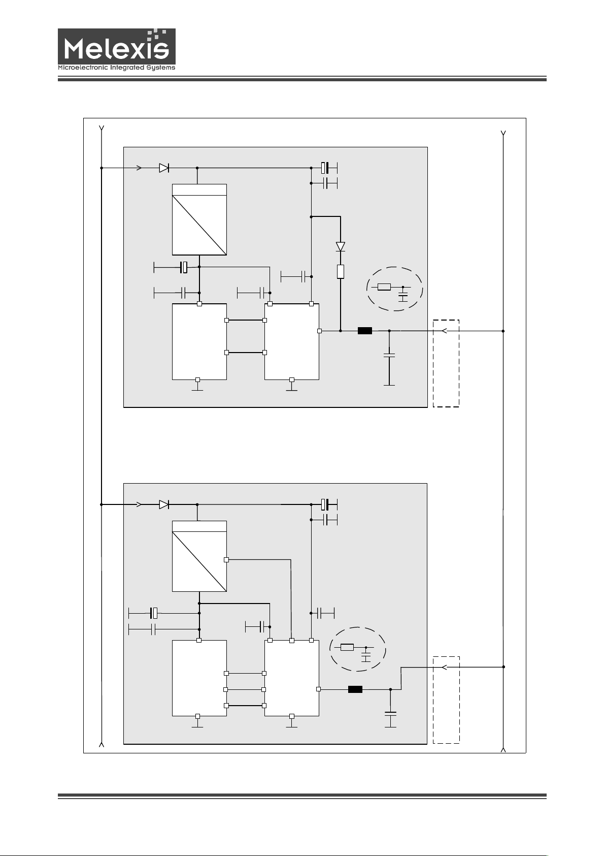
Application Circuit
100nF
TH8082
RxD
V
BAT
Voltage regulator
+5V
V
BAT
2.2uF1N4001
µP
VCC
ECU connector to
Single Wire LIN
Bus
BUS
33µH
82pF
TxD
VS
100nF
TH8080
[1]
RxD
V
BAT
Voltage regulator
+5V
V
BAT
2.2uF1N4001
µP
VCC
ECU connector to
Single Wire LIN
Bus
BUS
33µH
82pF
TxD
GND
VS
Car Battery
SLAVE
ECU
MASTER
ECU
100nF
GND
GNDGND
100nF
100nF
100nF
100nF
100nF
LIN BUS
EN
100p
10
optional
100p
10
optional
INH
INH
[1] TH8080 - low cost transceiver without INH control
Figure 2 - Application Circuit

TH8082
Single LIN Transceiver
www.melexis.com
Page 5 Data Sheet Rev 1.0 June 2001
Operating Conditions
Electrical Specification
All voltages are referenced to ground (GND). Positive
currents flow into the IC. The absolute maximum ratings
given in the table below are limiting values that do not
lead to a permanent damage of the device but exceeding
any of these limits may do so. Long term exposure to limiting values may affect the reliability of the device. Reliable operation of the TH8082 is only specified within the
limits shown in ”Operating conditions”.
Absolute Maximum Ratings
Parameter Symbol Min Max Unit
Battery voltage VS 6 18 V
Supply voltage V
CC
4.5 5.5 V
Operating am bient temp erature T
A
-40 +125 °C
Junction temperature
[1]
T
Jc
+150 °C
______________________________
Parameter Symbol Conditions Min. Max. Unit
Batterry Supply Voltage V
S
t < 1 min -0.3 + 30 V
-0.3 +7
Load dump; t<500ms +40
Transient supply voltage V
S.tr1
ISO 7637/1 pulse 1
[1]
-150 V
ISO 7637/1 pulses 2
[1]
+100
Transient supply voltage V
S.tr3
ISO 7637/1 pulses 3A, 3B -150 +150 V
BUS voltage V
BUS
t < 500 ms, VS = 20 V
V
S
= 20 V
-20
-40
+40 V
Transient bus voltage V
BUS.tr1
ISO 7637/1 pulse 1
[2]
-150 V
Transient bus voltage V
BUS.tr2
ISO 7637/1 pulses 2
[2]
+100 V
Transient bus voltage V
BUS.tr3
ISO 7637/1 pulses 3A, 3B
[2]
-150 +150 V
DC voltage on pins TxD, RxD V
DC
-0.3 +7 V
ESD capability of pin BUS ESD
BUSHB
Human body model, equivalent -4 +4 kV
ESD capability of any other pins ESD
HB
Human body model, equivalent -2 +2 kV
Maximum latch – up fr ee current at any Pin I
LATCH
-500 +500 mA
Maximum power dissipation P
tot
At T
amb
= +125 °C 197 mW
Thermal impedance
Θ
JA
in free air 152 K/W
Storage temp erature T
stg
-55 +150 °C
Junction temperature T
vj
-40 +150 °C
Supply Voltage
Short-term supply voltage
V
CC
V
S.ld
V
V
Transient supply voltage V
S.tr2
V
 Loading...