

MELEXIS TH8080JDC Datasheet
TH8080
D
Single LIN Bus
Features and Benefits
Single wire LIN transceiver
Compatibl e to LIN Protoc ol S pec ification, Rev. 1.1
Compatible to ISO9141 functions
Up to 20 kbps bus speed
Low RFI due to slew rate contr ol
Fully integrated receiver filter
Protection against load dump, jump start
Bus terminals proof against short-cir c uits and transients in the
Transceiver
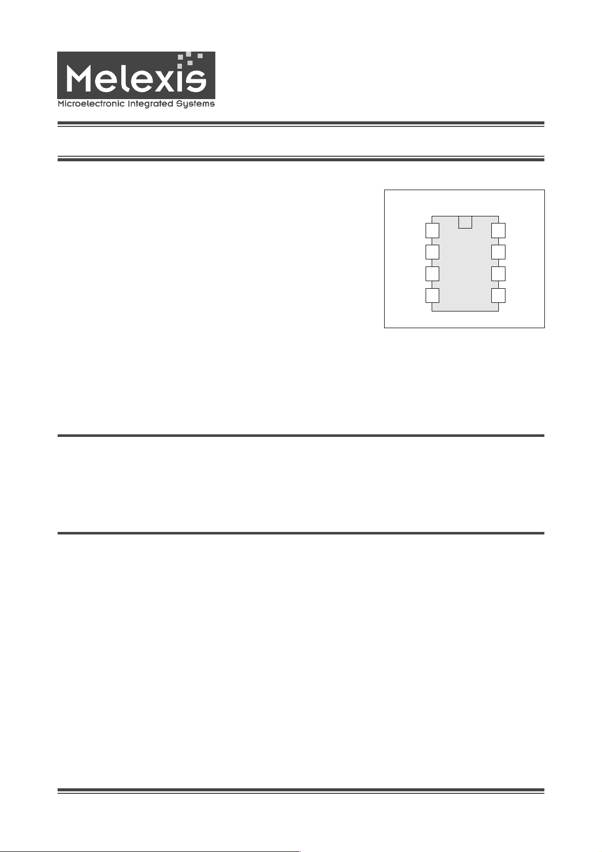
Pin Diagram
SOIC8NB
RxD
N.C.
TxD
1
2
TH8080
3
4
N.C.
8
VS
7
BUSVCC
6
5
GN
automotiv e environment
Very low (30 µA) typical power consum ption in recessive state and t her efore no sleep mode necessary
Thermal ov erl oad and short ci r c uit pr otection
High impendance Bus pin in case of loss of ground and undervoltage c ondition
8-pin SOIC
±4kV ESD protecti on on B us pi n
Ordering Information
Part No. Temperature Rang e Package
TH8080 JDC -40ºC...125ºC SOIC8, 150mil
General Descri ption
The TH8080 is a physical layer device for a single wire
data link capable of operating in applications where high
data rate is not required and a lower data rate can
achieve cost reductions in both the physical media components and in the microprocessor which use the network. The TH8080 is designed in accordance to the
physical layer definition of the LIN Protocol Specification , Rev. 1.1 . The IC furthermore can be used in
ISO9141 systems.
Because of the very low current consumption of the
TH8080 in the recessive state it’s particularly suitable for
ECU applications with hard standby current requirement s , whereby no sl eep/wake up co ntrol due to the
microprocessor is necessary.
Page 1 Target Data Sheet Rev 1.0 November 2000
www.melexis.com
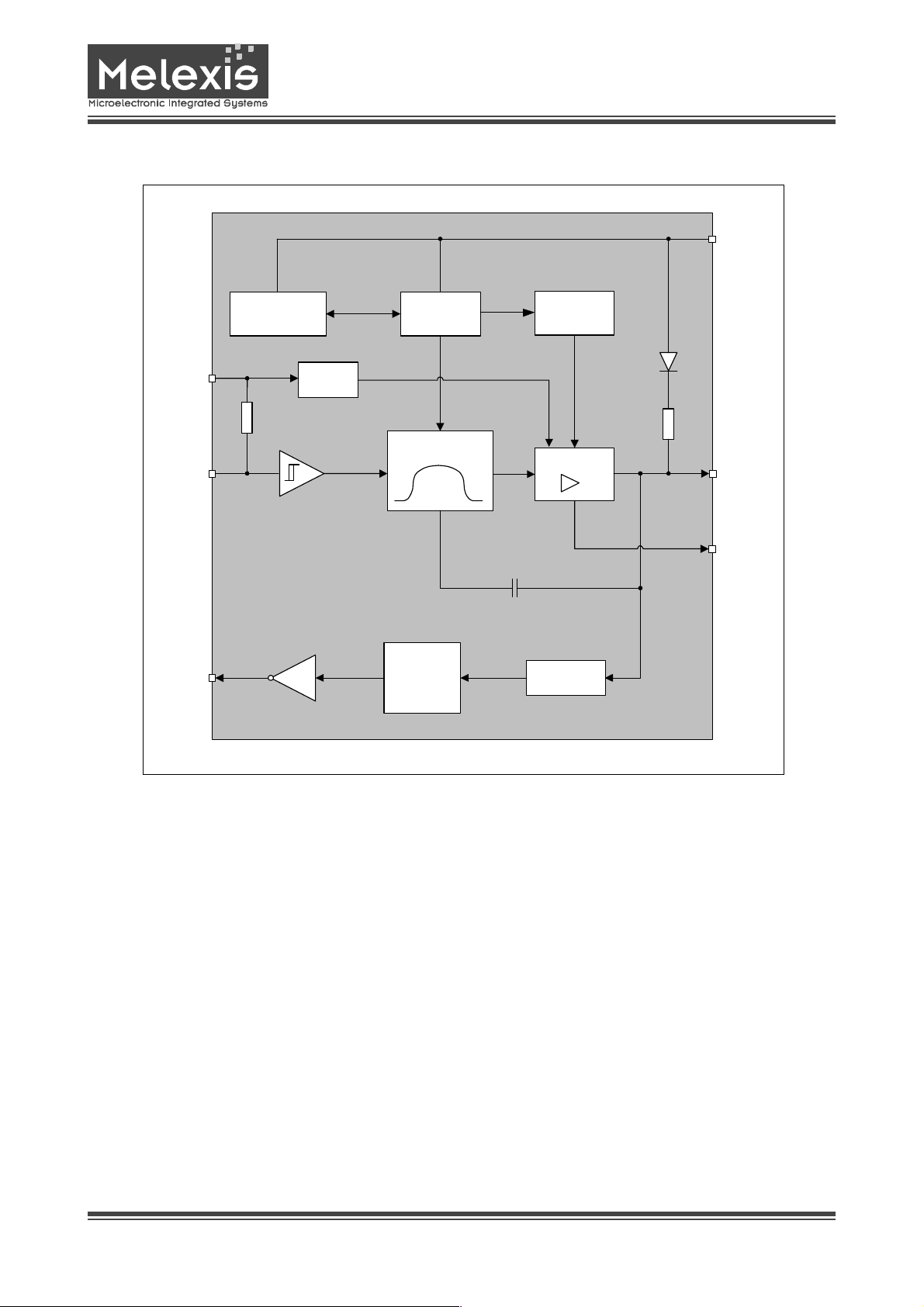
Functional Diagram
TH8080
Single LIN Transceiver
VS
VCC
TxD
RxD
interna l Supply
&
References
POR
Biasing &
Bandgap
SLEW RATE
Receive
Comparator
Thermal
Protection
BUS Driver
Input
Filter
BUS
GND
Figure 1 - Block Diagram
Page 2 Target D ata Sheet Rev 1.0 Nov. 2000
www.melexis.com
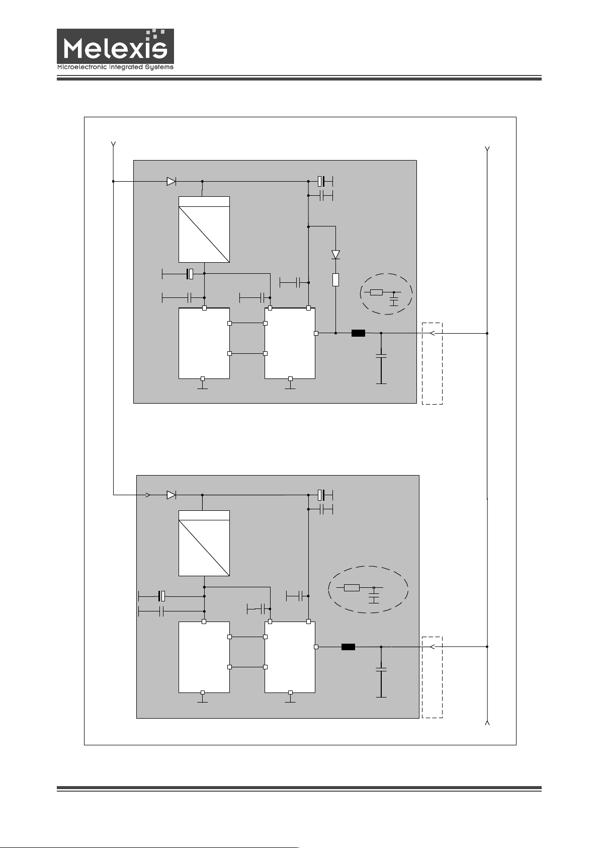
Application Circuit
TH8080
Single LIN Transceiver
Car Battery
V
BAT
100nF
Voltage regulator
V
BAT
+5V
µP
GND
100nF
VCC
RxD
TH8080
TxD
100nF
GND
LIN BUS
2.2uF1N4001
MASTER
100nF
VS
BUS
33µH
ECU
optional
10
100p
ECU connector to
Single Wire LIN Bus
2.2uF1N4001
V
BAT
Voltage regulator
+5V
100nF
µP
GND
100nF
V
BAT
optional
100nF
100nF
VS
VCC
RxD
BUS
TH8080
TxD
GND
SLAVE
ECU
10
100p
33µH
82pF
ECU connector to
Sin gle Wi re LIN Bus
Figure 2 - Application Circuit
Page 3 Target D ata Sheet Rev 1.0 Nov. 2000
www.melexis.com
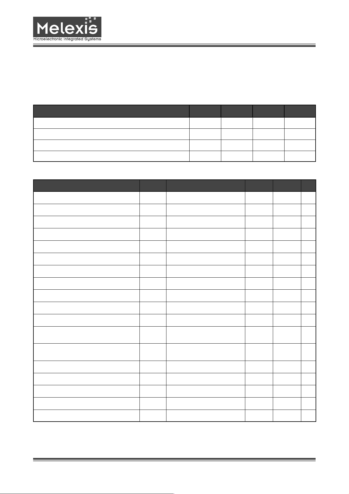
Electrical Specification
TH8080
Single LIN Transceiver
All voltages are referenced to ground (GND). Positive
currents flow into the IC. The absolute maximum ratings
given in the table below are limiting values that do not
lead to a permanent damage of the device but exceeding
any of these limits may do so. Long term exposure to limiting values may affect the reliability of the device. Reliable operation of the TH8080 is only specified within the
limits shown in ”Operating conditions”.
Operating Conditions
Parameter Symbol Min Max Unit
Battery voltage VS 6 20 V
Supply voltage V
Operating am bient temp erature T
Junction temperature
[1]
T
4.5 5.5 V
CC
-40 +125 °C
A
+150 °C
Jc
Absolute Maximum Ratings
Parameter Symbol Conditions Min. Max. Unit
Batterry Supply Voltage V
Supply Voltage
Short-term supply voltage
V
V
Transient supply voltage V
Transient supply voltage V
-0.3 +27 V
S
-0.3 +7
CC
Load dump; t<500ms +40
S.ld
ISO 7637/1 pulse 1
S.tr1
ISO 7637/1 pulses 2
S.tr2
[1]
[1]
-150 V
+100
V
V
V
Transient supply voltage V
BUS voltage V
Transient bus voltage V
Transient bus voltage V
Transient bus voltage V
S.tr3
BUS
BUS.tr1
BUS.tr2
BUS.tr3
DC voltage on pins TxD, RxD V
ESD capability of pin BUS ESD
ESD capability of any other pins ESD
Maximum latch – up fr ee current at any Pin I
LATCH
Maximum power dissipation P
Thermal impedance
Θ
Storage temp erature T
Junction temperature T
ISO 7637/1 pulses 3A, 3B -150 +150 V
-40 +40 V
ISO 7637/1 pulse 1
ISO 7637/1 pulses 2
ISO 7637/1 pulses 3A, 3B
-0.3 +7 V
DC
Human body model, equivalent
BUSHB
to discharge 100pF with 1.5kΩ
Human body model, equivalent
HB
to discharge 100pF with 1.5kΩ
[2]
[2]
[2]
-150 V
+100 V
-150 +150 V
-4 +4 kV
-2 +2 kV
-500 +500 mA
At T
tot
JA
stg
-40 +150 °C
vj
= +125 °C 197 mW
amb
in free air 152 K/W
-55 +150 °C
______________________________
[1]
ISO 7637 test pu lses are appl ied to VS via a rever se polar it y di ode and >1uF bloc king cap acit or .
[2]
ISO 7637 test pulses are app li ed to BUS via a coup li ng c apacitance of 1 nF.
Page 4 Target D ata Sheet Rev 1.0 Nov. 2000
www.melexis.com
 Loading...