

MELEXIS TH8061JDC Datasheet
Features and Benefits
LIN-Bus Transceiver:
PNP-bipolar transistor driver with slew rate control and current
limitation
BUS input voltage -24V ... 30V (independently of V
SUP
)
Possibility of BUS wake up
Baud rate up to 20 kBaud
Operating v oltage V
SUP
= 5.5 ... 18 V
Very low standby current consumption < 110 µA in normal mode (< 50 µA in sleep mode)
Linear low drop voltage regulator:
Output voltage 5V± 1%
Output current max. 50mA
Output current limitation
Overtemperature shutdown
Reset time 100ms and reset threshold voltage 4.65V
Load dump protected (40V)
Wake-up by LIN BUS traffic and start-up capable independent of EN voltage level
CMOS compatible interface to microcontroller
Ordering Information
Part No. Temperature Rang e Package
TH8061 JDC -40ºC...125ºC SOIC8, 150mil
General Descri ption
The mini-ReLIN TH8061 is the low cost variant of our
ReLIN-IC TH8060.
It consists a low drop voltage regulator 5V/50mA and a
LIN Bus Transceiver. The LIN-Transceiver is suitable for
LIN-Bus systems conform to “LIN-Protocol Specification”
Rev.1.1. from 04/17/2000.
TH8061
LIN Bus Transceiver with integrated Voltage Regulator
www.melexis.com
Page 1 Datasheet Rev 1.2 Feb 2001
The combination of voltage regulator and bus transceiver
make it possible to develop simple, but powerful and
cheap slave nodes in LIN Bus systems.
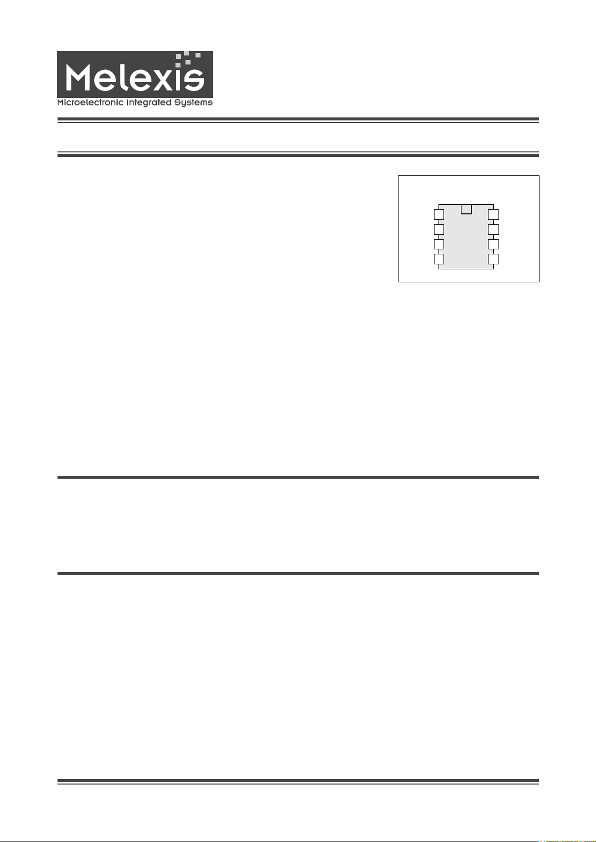
TH8061
1
EN RESET
BUS
GND
RxD
TxD
8
7
6
54
2
3
VSUP VCC
SOIC8NB
Pin Diagram
TH8061
LIN Bus Transcei ver w ith integrated Voltage Regulat or
www.melexis.com
Page 2 Datasheet Rev 1.2 Feb 2001
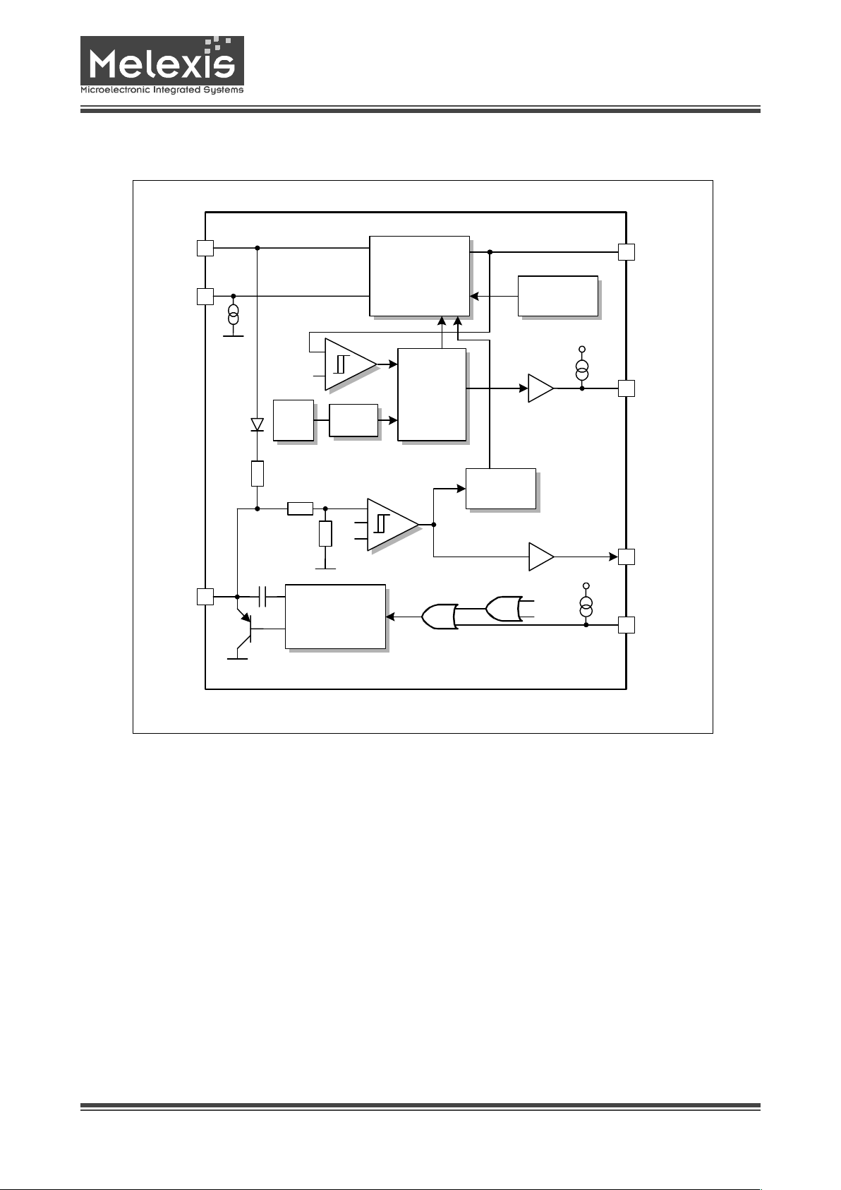
Functional Diagram
Figure 1 - Block Diagram
Reset
Wake-up
pnp Control
slew rate
foldback
OSC
Over Temp
V
thH
V
thL
+5V
VSUP
EN
BUS
RxD
TxD
RESET
VCC
30k
MR
TSHD
Power Supply
100ms
4.65V
+5V
TH8061
LIN Bus Transcei ver w ith integrated Voltage Regulat or
www.melexis.com
Page 3 Datasheet Rev 1.2 Feb 2001
Functional Description
The TH8061 consists a low drop voltage regulator
5V/50mA and a LIN Bus transceiver, which is a bi-
directional bus interface device for data transfer between
LIN-Bus and the LIN protocol controller.
Transmit Mode
During the transmission the data at the pin TxD will be
transferred to the pin BUS. To minimize the electromag-
netic emission of the bus line, the TH8061 has an integrated sl ew rate control.
pnpControl
slew rate
I
B
foldback
+5V
BUS
RxD
TxD
t
debBUS
t
debWAKE
BIAS
to wake up logic
V
thH
V
thL
ESD
MR
TSH D
VSUP
30k
Figure 2 - Block Diagram LIN Bus Transceiver
TxD
BUS
V
BAT
V
SUP
0.8 V
BAT
V
Diode
recessive
0.2 V
BAT
dominant
Figure 3 - Transmit Mode Pulse Diagram
LIN-BUS Transceiver
The TH8061 is a bi-directional bus interface device for
data transfer between LIN-Bus and the LIN protocol controller.
The transceiver consists a pnp-driver (1.2V@40mA) with
slew rate control and fold-back characteristic and consists as well in the receiver a high voltage comparator
followed by a debouncing unit.
The BUS pin has an integrated 30k pull up resistor with a
diode, which prevent the reverse current of VBUS during
differential voltage between VSUP and BUS (V
BUS>VSUP
).
TH8061
LIN Bus Transcei ver w ith integrated Voltage Regulat or
www.melexis.com
Page 4 Datasheet Rev 1.2 Feb 2001
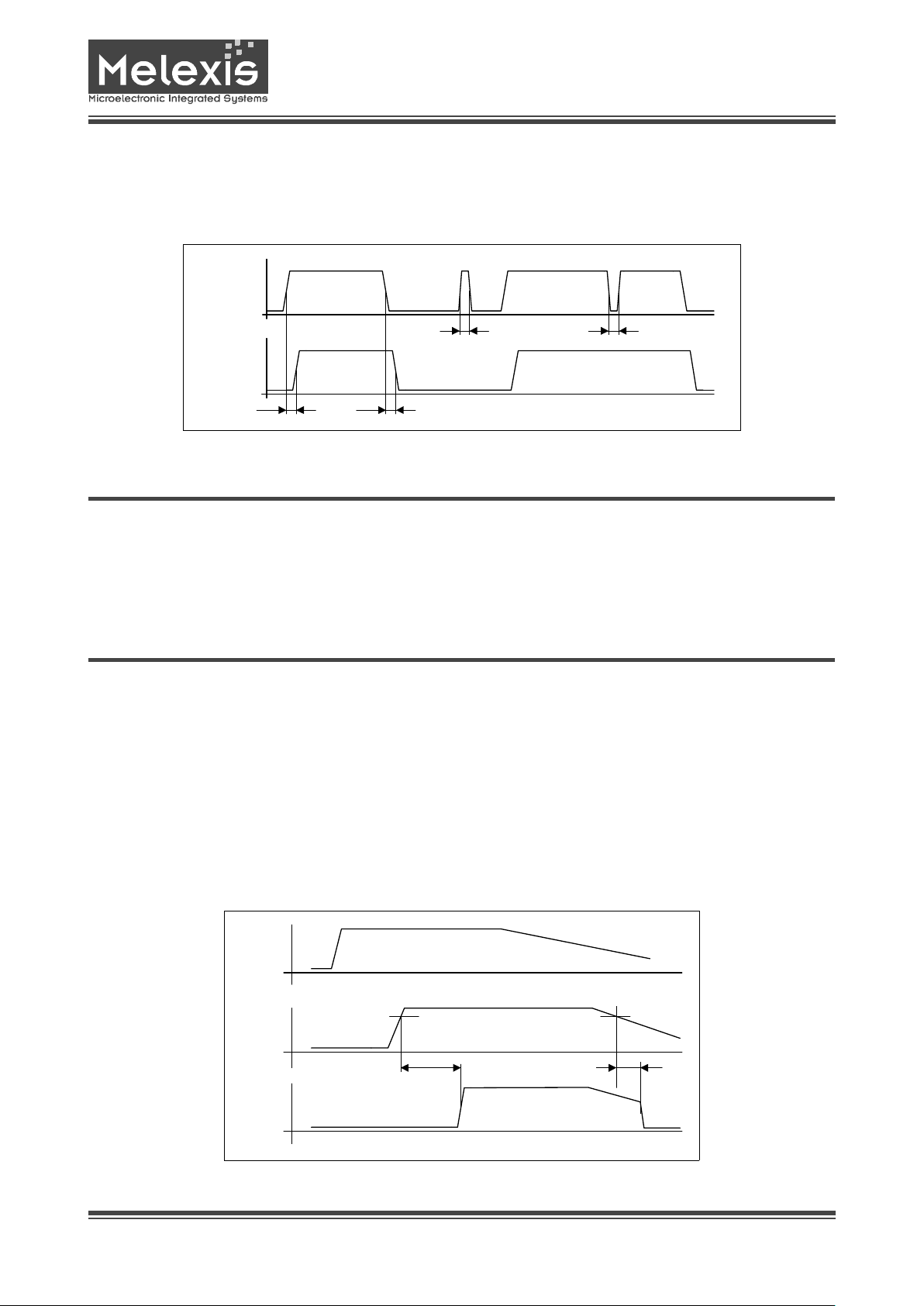
Receive Mode
The data at the pin BUS will be transferred to the pin
RxD. Short spikes on the bus signal are suppressed by
the implemented debouncing circuit.
Linear Regulator and Controlling Functions
Regulator
The TH8061 has an integrated linear regulator with an
output voltage of 5V ±2% and an output current of
BUS
RxD
t
debL
t < t
debL
t < t
debH
t
debH
Figure 4 - Block Diagram LIN Bus Transceiver
≤50mA. The regulator is switched on or off with a signal
on the EN pin or wake up with a BUS signal.
VS
VCC
t
RES
V
RES
t
rr
V
RES
RESET
Figure 5 - Initialization and Undervoltage
Initialization
The initialization is started if the power supply is switched
on, or after the temperature limitation has switched off
the regulator or in case of BUS traffic (wake up).
If the V
CC
voltage level is higher than V
RES
=4.65V, the re-
set time t
RES
= 100ms is started. After t
RES
a rising edge
on the RESET output is generated (see figure Initialization).
If V
CC>VPOR
the bus-interface will be activated.
The regulator is active and can only switched off with a
falling edge on EN. The regulator remain with EN=high in
active mode and therefore also the V
CC
voltage is active.
The input EN has an internal pull down resistor. If
EN=high, the internal pull down current is switched off to
minimize the quiescent current.

TH8061
LIN Bus Transcei ver w ith integrated Voltage Regulat or
www.melexis.com
Page 5 Datasheet Rev 1.2 Feb 2001
Temperature Limitation
If the Junction temperature 150ºC < Tj < 170ºC the over
temperture recognition will be active and the regulator
voltage will be switched off. After T
j
fall below 140ºC the
TH8061 will be initialized, not depending on of the voltage levels on EN and BUS.
Wake up with BUS traffic
If the regulator is put in standby mode it can be wake up
with the BUS interface. Every pulse on the BUS (high
pulse or low pulse) with a pulse width of min. 45µs will
switch on the regulator.
RESET Output
The RESET output is switched from low to high if V
SUP
is
switched on and V
CC>VRES
after the time t
RES.
If the voltage VCC drop below V
RES
then the RESET output is
switched from high to low after the tim e trr has been reached.
The voltage level for the RESET output is 4,65V and the
corresponding reset time t
RES
is 100ms.
After the BUS has wake up the regulator, it can only be
switched off with a high level followed by a low level on
the EN pin.
The function of the TH8061 is possible between T
Amax
and the switch off temperature, but small parameter differences can appear.
 Loading...