

MELEXIS TH8060JDF Datasheet
Features and Benefits
LIN-Bus Transceiver:
PNP-open emitter driver with slew rate control and current limita-
tion
BUS input voltage -24V ... 30V (independently of V
SUP
)
Possibility of BUS wake up
Baud rate up to 20 kBaud
Operating v oltage V
SUP
= 5.5 ... 18 V
Very low standby current consumption < 110 µA in normal mode
(< 50 µA in sleep mode)
Linear low drop voltage regulator:
Output voltage 5V± 1%
Output current max. 100mA
Output current limitation
Overtemperature shutdown
Configurable reset time (15ms/100ms) and reset threshold voltage (3.15V / 4.65V)
Low voltage detection at VSUP
Wake-up by LIN BUS traffic and start-up capable independent of EN voltage level
Universal comparator with an input voltage range –24V … 30V
and digital output
Load dump protected (40V)
Ordering Information
Part No. Temperature Rang e Package
TH8060 JDF -40ºC...125ºC SOIC16, 300mil
General Descri ption
The RELIN TH8060 consists a low drop voltage regulator
5V/100mA and a LIN Bus transceiver. The LIN-
transceiver is suitable for LIN-Bus systems conform to
“LIN-Protocol Specification” Rev.1.1. from 04/17/2000.
The combination of voltage regulator and bus transceiver
in combination with the monitoring functions make it
TH8060
1
EN SENSE
GND
GND
VTR
GND
GND
RESET
BUS
SO
SI
n.c.
RxD
TxD
16
15
14
13
12
11
10
98
7
6
5
4
2
3
VSUP VCC
SOIC16
TH8060
LIN Bus Transceiver with integrated Voltage Regulator
Pin Diagram
www.melexis.com
Page 1 Datasheet Rev 1.1 March 2001
possible to develop simple, but powerful and cheap
slave nodes in LIN Bus systems.
The wide output current area and the configurable reset
time and reset voltage works together with many differ-
ent microcontrollers.
TH8060
LIN Bus Transcei ver w ith integrated Voltage Regulat or
www.melexis.com
Page 2 Datasheet Rev 1.1 March 2001
Functional Diagram
Wake-up
pnp Control
slew rate
foldback
OSC
Over Temp
V
THSI _H
V
THSI _L
V
thH
V
thL
+5V
7.8V
6.8V
+5V
VSUP
EN
VTR
BUS
SI
SO
RxD
TxD
RESET
SENSE
VCC
30k
MR
TSHD
Power Supply
+5V
Reset-Logic
VTR-Logic
Figure 1 - Block Diagram

TH8060
LIN Bus Transcei ver w ith integrated Voltage Regulat or
www.melexis.com
Page 3 Datasheet Rev 1.1 March 2001
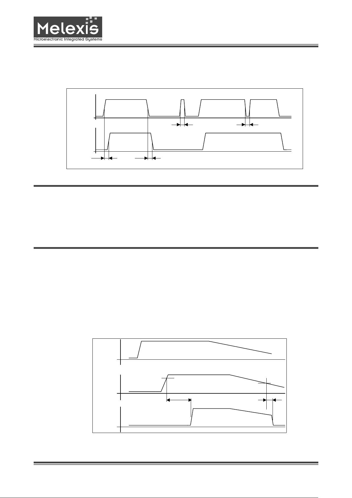
Functional Description
TxD
BUS
V
BAT
V
SUP
0.8 V
BAT
V
Diode
recessive
0.2 V
BAT
dominant
Figure 3 - Transmit Mode Pulse Diagram
The TH8060 consists a voltage regulator 5V/100mA and
a LIN Bus transceiver, which is a bi-directional bus interface device for data transfer between LIN-Bus and the
LIN protocol controller.
Also integrated into the transceiver are a voltage and
time controlled reset management, power down, wake
up function and a universal comparator for extended applications.
LIN-BUS Transceiver
The TH8060 is a bi-directional bus interface device for
data transfer between LIN-Bus and the LIN protocol
controller.
The transceiver consists a pnp-driver (1.2V@40mA) with
slew rate control and fold-back characteristic and con-
sists as well in the receiver a high voltage comparator
followed by a debouncing unit.
The BUS pin has an integrated 30k pull up resistor with a
diode, which prevent the reverse current of VBUS during
differential voltage between VSUP and BUS (V
BUS>VSUP
).
Transmit Mode
During the transmission the data at the pin TxD will be
transferred to the pin BUS. To minimize the electromag-
netic emission of the bus line, the TH8060 has an integrated sl ew rate control.
pnpControl
slew rate
I
B
foldback
+5V
BUS
RxD
TxD
t
debBUS
t
debW AKE
BIAS
to wake up logic
V
thH
V
thL
ESD
MR
TSHD
VSUP
30k
Figure 2 - Block Diagram LIN Bus Transceiver
TH8060
LIN Bus Transcei ver w ith integrated Voltage Regulat or
www.melexis.com
Page 4 Datasheet Rev 1.1 March 2001
BUS
RxD
t
debL
t < t
debL
t < t
debH
t
debH
Figure 4 - Block Diagram LIN Bus Transceiver
VS
VCC
t
Res
V
RESEIN
t
rr
V
RES1/2
RESET
Figure 5 - Init ia liz a tion
Receive Mode
The data at the pin BUS will be transferred to the pin
RxD. Short spikes on the bus signal are suppressed by
the implemented debouncing circuit.
Linear Regulator and Controlling Functions
Regulator
The TH8060 has an integrated linear regulator with an
output voltage of 5V ±2% and an output current of
≤100mA. The regulator is switched on or off with a signal
on the EN pin or wake up with a BUS signal.
Initialization
The initialization is started if the power supply is switched
on, or after the temperature limitation has switched off
the regulator or in case of BUS traffic (wake up).
If the V
CC
voltage level is higher than V
RESEIN
, the reset
time t
RES
is started. This reset time is determined by the
voltage level on the VTR pin (see table VTR Programming). After t
RES
a rising edge on the RESET output is
generated (see figure 10 - Initialization).
The regulator is active and can only switched off with a
falling edge on EN. The regulator remain with EN=high in
active mode and therefore also the V
CC
voltage is active.
The input EN has an internal pull down resistor. If
EN=high, the internal pull down current is switched off to
minimize the quiescent current.

TH8060
LIN Bus Transcei ver w ith integrated Voltage Regulat or
www.melexis.com
Page 5 Datasheet Rev 1.1 March 2001
RESET Output
The RESET output is switched from low to high if V
SUP
is
switched on and V
CC>VRESE IN
after the time t
RES.
If the voltage VCC drop below V
RES1
or V
RES2
then the RESET
output is switched from high to low after the time t
rr
has been
reached.
The voltage level for V
RES1
and V
RES2
or the correspond-
ing times t
RES
can be programmed via the analogue input
VTR.
Wake up with BUS traffic
If the regulator is put in standby mode it can be wake up
with the BUS interface. Every pulse on the BUS (high
pulse or low pulse) with a pulse width of min. 45µs will
switch on the regulator.
After the BUS has wake up the regulator, it can only be
switched off with a high level followed by a low level on
the EN pin.
Reset Programming on VTR
With the VTR pin the reset switch off levels and delay
time can be programmed.
The voltage on VCC influences the reset function.
VTR-Programming
The voltage on VTR input is read out if the voltage at this
pin is higher than V
RESEIN
. This value defines the reset
switch off voltage V
RES
and switches on with the next oscillator cycle the pull up current source if VTR=low or the
pull down current source if VTR=high. The sources are
active for one oscillator cycle. The level changes during
this procedures on VTR, wich depends on the external
pull up or pull down resistors control the reset tim e t
RR
Temperature Limitation
If the junction temperature 150ºC < Tj < 170ºC the over
temperture recognition will be active and the regulator
voltage will be switched off. After T
j
fall below 140ºC the
TH8060 will be initialized, not depending on of the voltage levels on EN and BUS.
Low Voltage Detectio n V
SUP
Low voltage on V
SUP
is monitored on SENSE output.
If V
SUP
has reached the level of V
SUP
=6.8V then the
SENSE output generates low level. In the normal
Universal Comparat or
The TH8060 consist a universal comparator for general
use. The positiv input of this comparator is connected
with the pin SI. The input voltage range of SI is 0V...V
SUP.
The function of the TH8060 is possible between T
Ama x
and the switch off temperature, but small parameter differences can appear.
operating range is V
SUP
> 7.8V and the SENSE output
generates a high level.
The input voltage is compared with a fixed reference
voltage at high or low level and the comparator output
SO drives a 5V digital signal.
VTR-Mode V
RES
t
Res
VTR = GND V
RES
= V
RES1
= 3.15V 100ms
VTR = VCC V
RES
= V
RES2
= 4.65V 100ms
VTR with R ≥ 50kΩ to GND
V
RES
= V
RES1
= 3.15V 15ms
VTR with R ≥ 50kΩ to VCC
V
RES
= V
RES2
= 4.65V 15ms
 Loading...